Recent progress of the ATLAS Planar Pixel Sensor R&D Project
Abstract
The foreseen luminosity upgrade for the LHC (a factor of 5-10 more in peak luminosity by 2021) poses serious constraints on the technology for the ATLAS tracker in this High Luminosity era (HL-LHC). In fact, such luminosity increase leads to increased occupancy and radiation damage of the tracking detectors.
To investigate the suitability of pixel sensors using the proven planar technology for the upgraded tracker, the ATLAS Planar Pixel Sensor R&D Project was established comprising 17 institutes and more than 80 scientists. Main areas of research are the performance of planar pixel sensors at highest fluences, the exploration of possibilities for cost reduction to enable the instrumentation of large areas, the achievement of slim or active edge designs to provide low geometric inefficiencies without the need for shingling of modules and the investigation of the operation of highly irradiated sensors at low thresholds to increase the efficiency.
In the following I will present results from the group, concerning mainly irradiated-devices performance, together with studies for new sensors, including detailed simulations.
keywords:
Silicon pixel detectors , planar sensors , radiation damage to detector materials (solid state) , detector simulations , ATLAS upgrade , HL-LHC , SLHC1 Introduction
ATLAS [1] is a general purpose detector for the study of primarily proton-proton collisions at the LHC [2].
The ATLAS Inner Detector [3, 4] provides charged-particle tracking with high efficiency over the pseudorapidity range . The pixel detector system [5] is the innermost element of the Inner Detector. The pixel detector contains approximately 80 million channels and provides pattern recognition capability in order to meet the track reconstruction requirements of ATLAS at the full luminosity of the LHC of .
Consisting of three barrel layers (at radii between 50.5mm and 122.5mm), and six discs, the pixel detector counts a total of 1744 pixel modules, which are mounted allowing for a three-hit track-reconstruction of charged secondary-particles. Each module contains a 250 m thick n-in-n pixel sensor of 62.6 18.6mm2 with pixel cells of 50400 . Connected to each sensor are 16 7.411.0mm2 ATLAS FE-I3 [6] readout chips with a total of 46080 channels. Both the sensors as well as the electronics of the present ATLAS pixel modules were specified to work up to a fluence of and an ionising dose of 50 MRad.
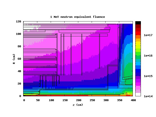
While the nominal luminosity of the present LHC accelerator is , an upgrade to increase the luminosity by a factor of ten (five with luminosity leveling) is planned to be carried out in a two phase process [7]. After a first shutdown, foreseen for 2017, the Phase 1 of LHC will start, with the goal luminosity of . A second shutdown will take place after 2020; then the Phase 2 will start, and the expected luminosity is with luminosity levelling. By 2030 a total integrated luminosity of is envisaged. Based on this scenario the innermost layer of the ATLAS pixel system will have to sustain fluences above [8]; see also figure 1.
The main effects on the pixel sensors from these large fluences are an increase of the leakage current and a reduction in the charge collection efficiency. The final goal is to retain a good hit-efficiency up to the final integrated luminosity.
Another high-luminosity related effect is the increase of the occupancy of the detector. A natural option is to reduce the size of the elementary pixel cell; at the same time the spatial resolution will improve. The reduced size of the elementary cell is just one of the features of the new read-out chip for the pixel system, the FE-I4 [9] chip; the total surface of the FE-I4 chip is 20.0 18.6 mm2. Moreover, replacing the strips of the Inner Detector with pixel detectors might be an option to handle the occupancies foreseen at the HL-LHC.
Hence, in view of a possible pixel system replacement in 2017; and then, maybe, for a whole new tracking system after 2020, a new Pixel System is unders study. The new pixel sensors will have not only to sustain the harsher environment, but also to show high geometrical acceptance: for the future the material budget restrictions and the geometrical limitations ask for geometry inefficiency to be below 2.5%. Hence the inactive areas of the future pixel sensor should be less than 450 m wide [10].
Different sensor options are being developed in parallel to address the challenges imposed by the forseen luminosity upgrades. They include diamond sensors [11] and 3D-sensors, with implants going through the silicon bulk [12]. Optimizing the well-known technology of planar silicon pixel sensors for the ATLAS detector at an upgraded LHC accelerator is carried out within the Planar Pixel Sensor project [13].
2 The project
Planar pixel sensors are the current technology for the ATLAS pixel system and a standard for tracking detectors in High Energy Physics. A lot of experience in designing, optimizing and producing planar sensors has been accumulated in the last 30 years; during these three decades planar sensors proved to be a reliable technology. There is still a lot of research on planar sensors and a lot of suppliers are on the market, assuring high quality and relatively low cost productions. Hence planar sensor are one good option for future tracking detectors. The ATLAS Upgrade Planar Pixel Sensor (PPS) R&D Project is a collaboration of 17 groups and more than 80 scientists aiming to explore the suitability of planar pixel sensors for the ATLAS upgrade.
Primary goal of the project is to demonstrate that planar sensors have the requested radiation hardness for the HL-LHC. To investigate this, several planar sensors technologies are under evaluation, including p-bulk (Section 3) and n-bulk (Section 4) option; regardless of the bulk, the group is looking only at sensors collecting electrons, based on their smaller trapping time compared to holes [14].
A reduction in sensor thickness (with respect to the 250 m of the current ATLAS pixels) is investigated (Section 5), to reduce the effects of trapping after irradiation and the material budget.
In case of a complete replacement of the Inner Detector a solution with more than 4 layers of pixels is possible. In this way an area of roughly 10 m2 should be equipped with pixel modules. Hence it is crucial to minimize the costs of the future pixel system. PPS is evaluating several cost-reduction scenarios, including new bump-bonding technologies, given the fact that the bump-bonding cost dominated the cost of the current ATLAS pixel detector. The possibility to use p-bulk sensor is favorable in the view of a cost reduction, having only one side patterned contrary to two-side patterned n-bulk sensors.
The new sensors will have to assure a close to 100% geometrical acceptance, so different options toward a reduction of the inactive area are pursued in the collaboration, such as slim edge geometries(Section 6) and active edge detectors (Section 7).
Many of the new ideas for sensors are tested in advance by means of sensor simulations (Section 8) thanks to a TCAD software.
In Section 9 the plans of the PPS R&D collaboration will be outlined, together with some general remarks on the work done so far.
3 P-bulk overview
In this Section a quick overview of the PPS activities on p-bulk sensors will be given.
Standard n-in-n sensors need guard-rings opposite to pixel side: the production requires to pattern both sides of the wafer. On the contrary, p-bulk does not need such a double processing, having only an homogeneous implantation on the back side. This should allow for a significant cost reduction. Another major advantage of p-bulk over n-bulk is that there is no type inversion for irradiated material [15].
A problem under investigation for the n-in-p detectors is the drop between the high voltage applied to the back side and the readout electronics potential ( 0V) which occurs solely on the sensor top side facing the readout electronics. In figure 2 a sketch of the p-bulk sensor geometry is displayed, highlighting the issue with the voltage drop on the sensor in a region close to the electronics.
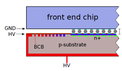
Covering the sensor with a thin layer of BCB (Benzo Cyclo Butene) proved to prevent sparks up to 1000 V.
Several contributors are working with p-bulk sensors in the PPS R&D group, namely CiS Forschungsinstitut für Mikrosensorik und Photovoltaik GmbH, Micron Semiconductor Ltd., Hamamatsu Photonics K.K. (HPK) and Max Planck Institut für Physik - Max Planck Institut Halbleiterlabor (MPI-HLL). A variety of sensor thicknesses is currently investigated by the different contributors. In table 1 a summary is given.
| Suppliers | Thickness () |
|---|---|
| CiS | 285/200/150 |
| Micron | 300/150 |
| HPK | 320/150 |
| MPI-HLL | 150/75 |
More details are given in [16].
4 N-bulk sensors: results for irradiated devices
To assess the radiation hardness of n-bulk sensors, irradiation campaigns have been carried out and crucial observables, such as the charge colleced per impinging particle and hit efficiency, were studied as a function of the delivered dose. In the following details on the studies performed on irradiated n-in-n sensors will be given.
The starting point for the PPS R&D project are the ATLAS single chip pixel modules [5]. Planar n-in-n ATLAS sensors, already assembled with a FE-I3 chip in a single chip module (SCM) were irradiated with neutrons at the TRIGA nuclear reactor [17] of the Jozef Stefan Institute in Ljubljana. Modules were irradiated with fluences up to and then characterized with radioactive sources and beams [18]. In figure 3 the two experimental setups are shown.
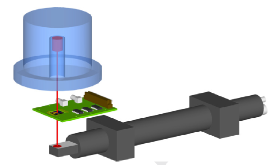
As displayed on the left, the 90Sr source was enclosed by a collimator. The module was cooled with dry ice and operated at temperatures below -50∘ C. A trigger scintillator was mounted below the SCM.
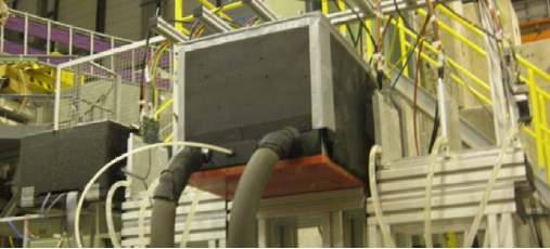
The SCMs were also operated in testbeams at the CERN SPS beamline (see figure 3, right) in July and October 2010. Thanks to the testbeam, it was possible to compare the energy depositions of high-energy pions with those of beta-electrons and to be able to observe the effect of different incidence angles after high fluences. The testbeam was conducted with the EUDET beam telescope [19] which uses six MIMOSA26 chips [20] as telescope planes. The six telescope planes were defining the tracks and up to six devices under test (DUTs) were put between the first and second telescope arm. The irradiated modules were cooled with dry ice; the operation temperature was kept between -35 and -15∘ C.
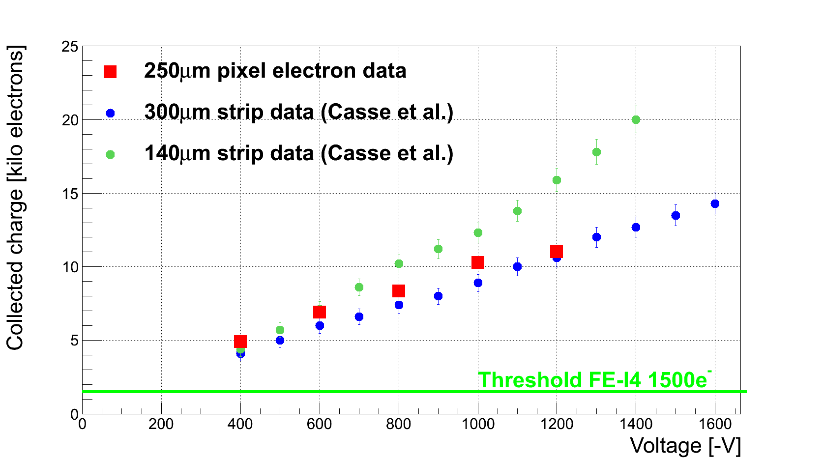
In figure 4, on the left, a study of the collected charge vs bias voltage for a module irradiated with a fluence of is shown222as a comparison data from [21] are reported too. (only data collected with the 90Sr are shown). In the figure the expected threshold for the FE-I4 chip is shows too. A signal of about 10 ke- is observed at 1000 V. This is very promising for the foreseen ATLAS pixel layer (“IBL”) [22], and the outer pixel layers at HL-LHC.
In figure 4, on the right, the hit-efficiency map for the module irradiated with a fluence of , as measured at the testbeam for particles at normal incidence. The SCM was biased at 1000 V and the hit-efficiency was 99.6%.
Hit efficiency was studied as a function of the bias voltage, for the module irradiated with . Results are in table 2.
| Bias voltage (V) | Hit efficiency (%) |
|---|---|
| 350 | 93.2 |
| 500 | 97.3 |
| 1000 | 99.6 |
The results for n-in-n devices indicate that for the second layer at HL-LHC, current pixel system is able to collect sensible amount of charge with efficiency close to 1.
The module irradiated with a fluence of was able to collect roughly 5500 electrons at 1500 V; the result is presented in figure 5. This remarkable result shows the possibility to still collect charge with planar detectors at the highest expected fluences of HL-LHC.
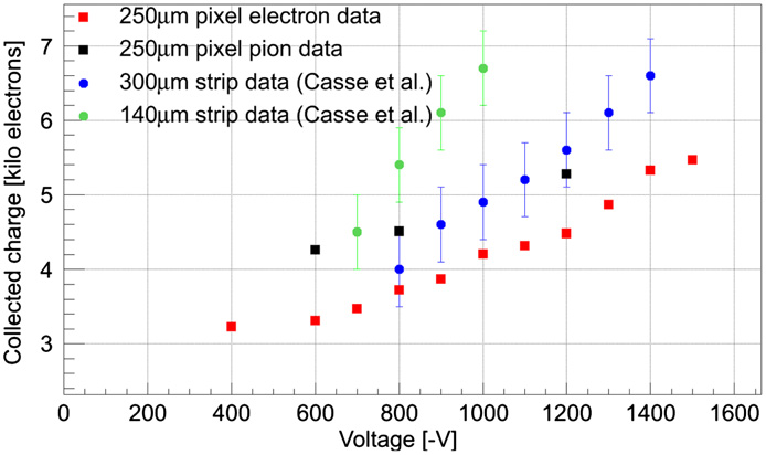
The results for the collected charge by the n-in-n irradiated module are summarized in table 3.
| Fluence () | Bias voltage (V) | Collected charge (10 ke-) |
| 1 | 1000 | 18 |
| 5 | 1000 | 10 |
| 20 | 1500 | 5.5 |
5 Thin production
While thin planar sensors yield lower - nonetheless sufficient - signals before irradiation, they offer several potential advantages compared to sensors with standard thicknesses. A reduction of the radiation length in silicon leads to less multiple scattering allowing for improvements in the tracking resolution. Furthermore, for the same voltage the electric field in thin sensors is higher. This seems to increase the signal size after irradiations by charge multiplication effects [24].
Recent results [25] indicate that with a 140 m thick sensor irradiated with it is possible to collect 12 thousand electrons at 1000 V, roughly 2000 electrons more than a standard 300 m thick planar sensor.
A dedicated n-wafer production with thicknesses ranging from standard 250 m down to 150 m has been competed at CiS. First modules have been assembled and are currently being irradiated. They will be used for detailed studies of charge collection and charge amplification.
6 Slim edge
In the present pixel sensor the distance between the active pixel area and the cutting edge is 1100 m. This was done to prevent the depletion area to reach the cut-edge.
The geometry of the future ATLAS pixel detector foresees no shingling in direction, and flat, single-sided staves for the inner radii, hence a reduction in sensor dead-area is required.
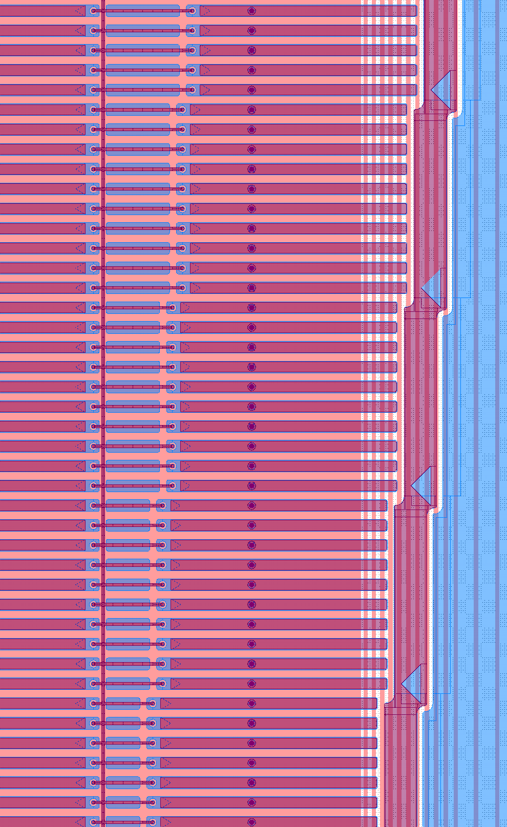
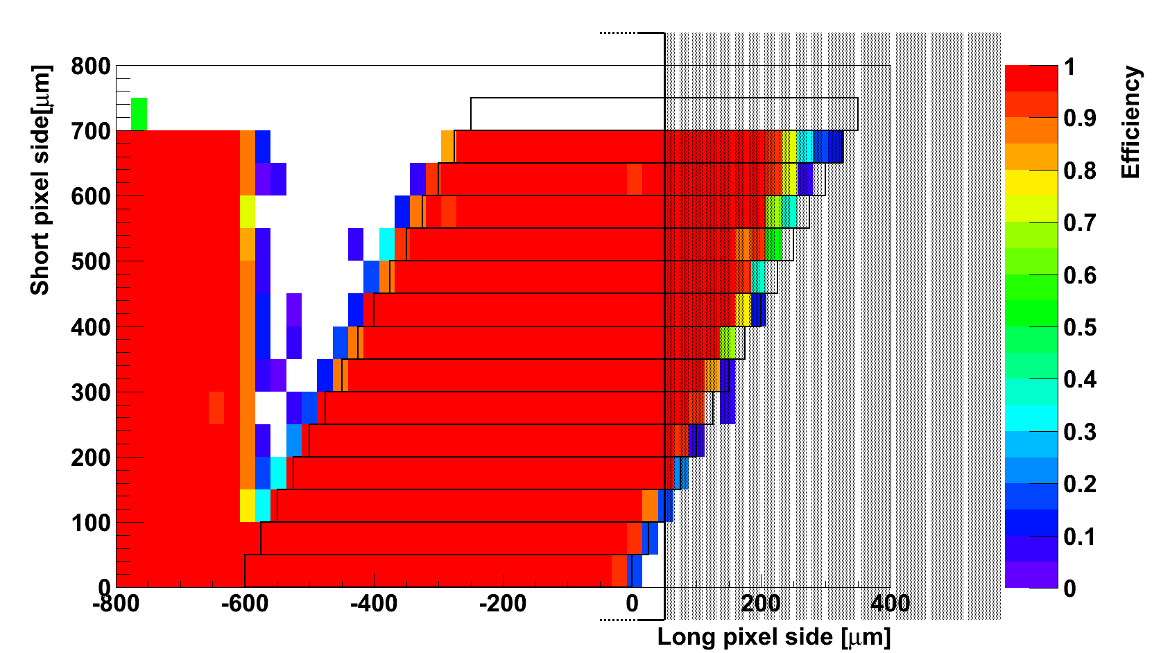
PPS studied an n-in-n pixel sensor in which the pixels close to the edge are longer than the standard ones, partially overlapping with the guard-ring region (“slim edge” design). A dedicated structure to this goal was prepared, with pixels shifted in a step-wise way (“stepwise pixel”) in order to see which was the minimum inactive area with still excellent hit-efficiency. In figure 6, on the left, the design of this detector is illustrated; dark red horizontal rectangles correspond to pixel implants, while light red vertical strips (at the right edge) represent guard-rings.
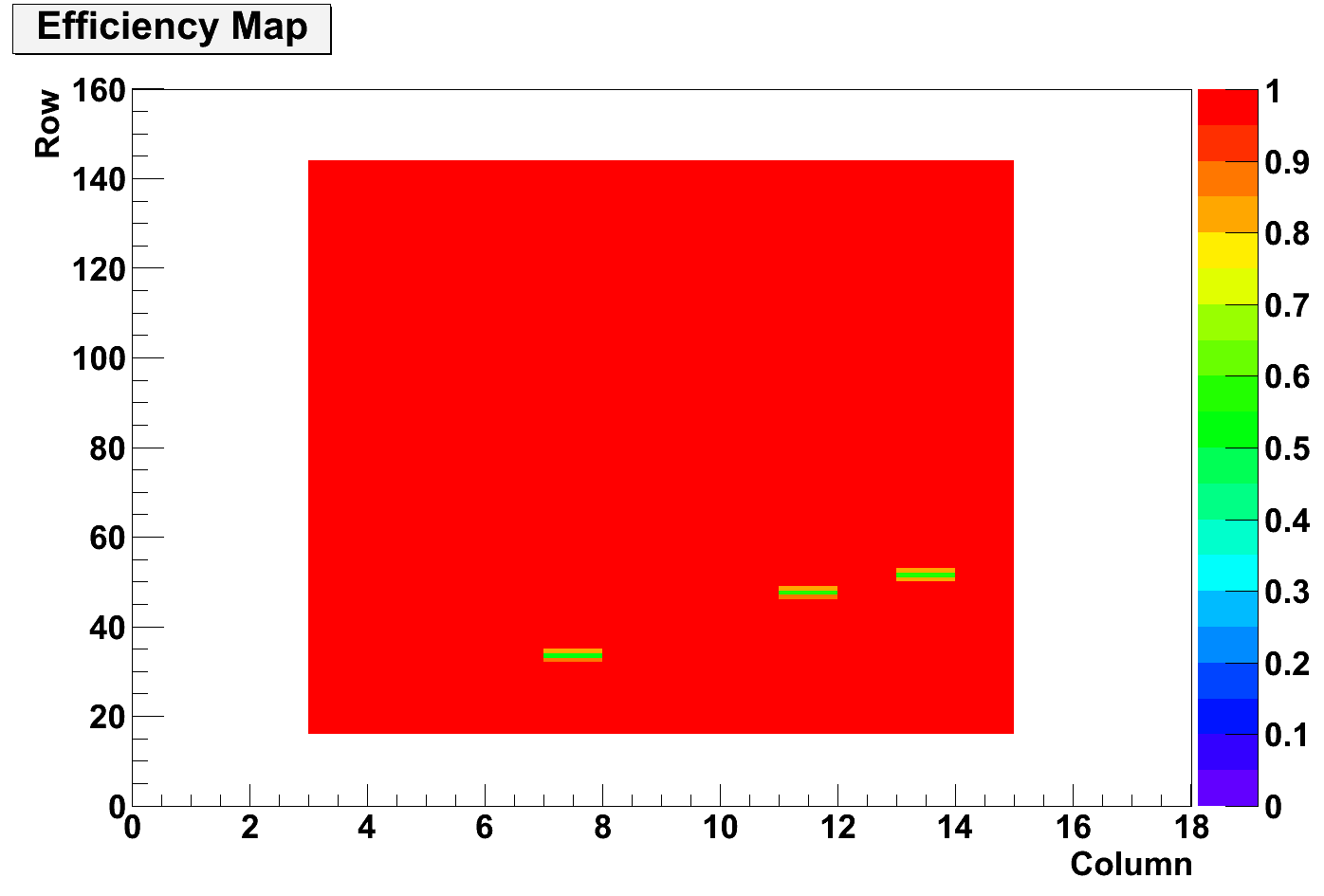
In figure 6, on the right, a hit-efficiency map (as observed at the testbeam mentioned in section 4) for a non-irradiated “stepwise” pixel detector is presented. The p+ implant on the back side ends at 0 and the grey part represents the guard-ring area (on the opposite side of the pixels), which is part of the “inactive” area in the standard design. It is clear that pixels are almost 100% efficient up to 200 m from the p+ implant edge, reducing in this way the inactive area to 250 m only.
7 Active edge
As already discussed detectors made using planar technology have an insensitive region around their edges to prevent the depletion region to reach the nonpassivated saw cuts at the detector edges and to allocate enough space for the guard rings [26]. Nonetheless reducing the inactive area between the edge pixels and the cut-edge is essential to maintain a high geometrical acceptance.
To control the potential drop along the cut edge, and then reduce the inactive area several “active edge” approaches are under study.
One possibility is to terminate the sensor with heavily doped trenches, where the insensitive edge region can be reduced to a few m; this technique was originally adopted by FBK for 3D sensors [27]. A trench is dug by Deep Reactive Ion Etching (DRIE), then it is doped and filled with polysilcon. This process allows the production of particularly thin sensors: thus it is very promising for inner HL-LHC pixel layers. Simulations carried inside the PPS collaboration indicate the possibility to realize an n-in-p detector with reduced dead area (few tens of m) and good stability, even after large irradiation.
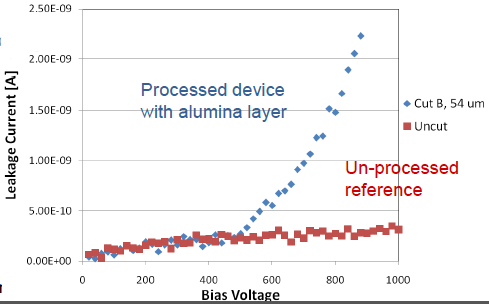
Another approach is to passivate the cutting edge by atomic layer deposition (ALD) [28]. A different approach for n-bulk and p-bulk sensor is used. In the former case a positively charged layer is envisaged, so a low-temperature oxide growth is performed; in the latter case a negatively charged layer is needed, and so an ALD of Al2O3 is done.
First test on diodes with only one guard ring [29] indicates no breakdown up to 500 V after the cut and stable current below 50 pA [28]; IV curve for this device is shown in figure 7.
The passivation of the trench is performed after cutting the sensor from the wafers (several cutting techniques are considered [30]). This feature makes this approach interesting for outer layers as it is possible to use with sensors from any vendor and type.
8 Advanced simulations
In the PPS project several simulation activities are ongoing, trying to identify possible ways to optimize the layout and improve the sensor performance.
The program Silvaco Technology Computer Aided Design (TCAD) [31] is used for simulating lithography and implantation parameters to model and evaluate various semiconductor designs and processes, helping in reducing the number of wafer submission by identifying early problematic layout configurations or potentially non-optimal process parameters.
The electrical characteristics of semiconductor devices are simulated starting from the definition of the processes to form the diode junction, such as oxidation of the bare bulk material, insulation implantation, oxide etching, acceptor/donor implantation for electrical contacts definition and so on. Once the structure of the semiconductor device is defined it is possible to simulate its behavior under several realistic situations, such as applied bias voltages, radiation-induced damages in the bulk and on the surface, illumination by laser, etc. All the relevant observables, such as currents, capacitance, distribution of electric potential and field, of free carriers and of space charge can be studied as a function of the model parameters.
The PPS project studied by means of Silvaco-TCAD simulation the behavior of the detector after irradiation, in relation to different designs for the multi-guardrings structures [32, 33]. The radiation damage was modeled by localized defects in the band gap of silicon. Several models exist; among them the one based on the RD50 collaboration results [34] and work of several groups [35, 36, 37].
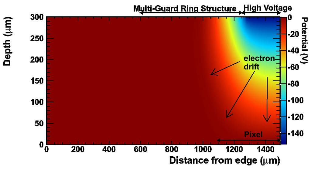
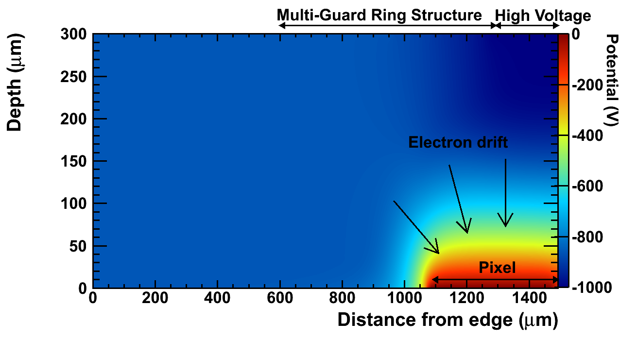
As an example of simulations application we show on figure 8 the results for slim edge design (see section 6); on both pictures the potential map is shown, before (left) and after (right) irradiation (fluence of ). We can observe that after irradiation the electric field lines are less distorted than before; this is a nice prediction reassuring us on the viability of the slim edge design even after large fluences.
9 Conclusions & Outlook
The ATLAS PPS R&D Project is trying to asses the radiation hardness of the planar pixel sensors, in view of the luminosity upgrade foreseen for the LHC (the so called HL-LHC era).
The PPS group is investigating both n- and p-bulk sensors. First sensor prototypes are been evaluated with radioactive source and on beams. Results for n-in-n devices indicate the viability of the technology (large signal collected for MIPs with close to 1 efficiency) even after irradiation at fluences up to (the expected fluence for outer pixel layers at HL-LHC). Pixels shown to collect sizable amount of charge even at , the expected fluence for the innermost pixel layers at HL-LHC.
The group is committed into inactive area reduction, to cope with the geometrical restrictions for future ATLAS tracker, keeping geometrical acceptance close to 1. Several approaches are investigated: a “slim edge” design, by pushing pixels beyond guard-ring boundary, and “active edge” techniques, which deal with the treatment of the trench at edge.
Several studies are stimulated first, and optimized then, by dedicate simulations of the proposed sensors.
New sensor designs are under way, which will be throughly tested with radioactive source and in beam, after irradiation; the final goal will be to prove that planar pixels can be the technology for the ATLAS tracker in the high luminosity LHC era, too.
References
- [1] G. Aad, et al., JINST 3 (2008) S08003. doi:10.1088/1748-0221/3/08/S08003.
-
[2]
LHC Technical Design
Report.
URL http://lhc.web.cern.ch/lhc/LHC-DesignReport.html -
[3]
ATLAS collaboration, Inner
detector - technical design report, 1, Tech. rep., CERN (1997).
URL http://cdsweb.cern.ch/record/331063 -
[4]
ATLAS collaboration, Inner
detector - technical design report, 2, Tech. rep., CERN (1997).
URL http://cdsweb.cern.ch/record/381263 - [5] G. Aad, M. Ackers, F. Alberti, M. Aleppo, G. Alimonti, et al., JINST 3 (2008) P07007. doi:10.1088/1748-0221/3/07/P07007.
- [6] I. Peric et al., Nucl. Instr. and Meth. A 565 (1) (2006) 178 – 187.
- [7] A. Tricomi, Nucl. Instr. and Meth. A 596 (1) (2008) 43 – 47.
- [8] M. Bruzzi et al., Nucl. Instr. and Meth. A 541 (1-2) (2005) 189 – 201.
- [9] M. Garcia-Sciveres et al., Nucl. Instr. and Meth. A 636 (2011) S155–S159.
-
[10]
ATLAS IBL Community,
Atlas
insertable b-layer technical design report, Tech. rep., CERN (2010).
URL http://cdsweb.cern.ch/record/1291633/files/ATLAS-TDR-01%9.pdf - [11] D. Asner et al., Nucl. Instr. and Meth. A 636 (2011) 125 – 129.
- [12] P. Hansson et al., Nucl. Instr. and Meth. A 628 (1) (2011) 216 – 220.
-
[13]
ATLAS Upgrage Planar Pixel Sensor
R&D Project.
URL https://edms.cern.ch/document/966140 - [14] G. Kramberger et al., Nucl. Instr. and Meth. A 481 (1-3) (2002) 297 – 305.
- [15] M. Moll, Radiation Damage in Silicon Particle Detectors, Ph.D. thesis, Hamburg (1999).
- [16] A. Macchiolo, these proceedings.
- [17] D. Zontar et al. , Nucl. Instr. and Meth. A 426 (1) (1999) 51 – 55.
- [18] S. Altenheiner et al., Nucl. Instr. and Meth. A, doi:{10.1016/j.Nucl.Instr.andMeth.A.2011.05.074}.
- [19] A. Bulgheroni et al, Nucl. Instr. and Meth.A 623 (2010) 399.
- [20] C. Hu-Guo, et al., Nucl. Instr. and Meth. A 623 (2010) 480.
- [21] G. Casse et. al, Nucl. Instr. and Meth. A 624 (2010) 401.
- [22] P. Grenier, these proceedings.
- [23] G. Casse et al., Nuclear Science, IEEE Transactions on 56 (3) (2009) 765 –770.
- [24] G. Kramberger et al., IEEE NSS Conference Record 1 (24) (2009) 1740 –1748.
- [25] G. Casse et. al, PoS(Vertex 2010).
- [26] C .J Kenney et al., IEEE Transactions on Nuclear Science, 48 (6) (2001) 2405–2410.
- [27] G. F. Dalla Betta et al., Nucl. Instr. and Meth. A 636 (1, Supplement 1) (2011) S15 – S23.
-
[28]
M. Christophersen,
Laser-Scribing and Sidewall
Passivation of P-Type Sensors.
URL {http://indico.cern.ch/getFile.py/access?contribId=7&s%essionId=1&resId=1&materialId=slides&confId=114255} - [29] Y. Unno et al., Nucl. Instr. and Meth. A 636 (1, Supplement 1) (2011) S24 – S30.
- [30] V. Fadeyev et al., Improving pixel detectors: Active area optimization and high temperature annealing, in: Nuclear Science Symposium Conference Record (NSS/MIC), 2009 IEEE, Vol. 24, 2009, pp. 1674 –1677.
-
[31]
Silvaco International Inc., 4701 Patrick
Henry Drive, Bldg 2 Santa Clara, CA 95054.
URL {http://www.silvaco.com/} - [32] G. Calderini et al., Nucl. Instr. and Meth. A 636 (1, Supplement 1) (2011) S37 – S41.
- [33] M. Benoit et al., JINST 4 (2009) P03025.
-
[34]
M. Bruzzi and M. Moll, Tech. rep., CERN, RD50 status report (2007).
[link].
URL {http://cdsweb.cern.ch/record/1082083/files/RD50statusr%%****␣bomben_tipp11.bbl␣Line␣150␣****eport.pdf} - [35] F. Moscatelli et al., Nucl. Instrum. Meth. B 186 (2002) 171.
- [36] F. Moscatelli et al., IEEE Trans. Nucl. Sci. 51 (4) (2004) 1759–1765.
- [37] F. Moscatelli et al., Nucl. Instrum. Meth. A 563 (1) (2006) 192–195.