Design of Metamaterial Surfaces with Broad-band Absorbance
Abstract
A simple design paradigm for making broad-band ultra-thin plasmonic absorbers is introduced. The absorber’s unit cell is composed of sub-units of various sizes, resulting in nearly 100% absorbance at multiple adjacent frequencies and high absorbance over a broad frequency range. A simple theoretical model for designing broad-band absorbers is presented. It uses a single-resonance model to describe the optical response of each sub-unit and employs the series circuit model to predict the overall response. Validity of the circuit model relies on short propagation lengths of the surface plasmons.
Plasmonic metamaterials (MMs) are subwavelength metallic nanostructures designed to provide extraordinary electromagnetic properties in specified frequency ranges Lindell_2001 ; schurig_prl2003 . The combination of the plasmonic response of conduction electrons and appropriate (but not necessarily geometrically complicated) design of the structures results in subwavelength feature sizes and strong near-field enhancement. These properties pave the way to various applications, such as surface enhanced Raman scattering Fei_2008 ; Paul_2008 , light trapping Atwater_NM2010 , bio-molecule sensing adato_pnas09 , and plasmonic absorbers padilla_prl08 ; wu_spie08 ; avitzour_prb09 ; giessen_nl10 ; padilla_apl10 ; wu_2011 . For the reasons going beyond the simplicity of fabrication, many applications utilize MM surfaces instead of MMs. For example, MM surfaces provide solid/liquid interfaces for bio-sensing, or can be used as ultra-thin coatings to provide spectrally-selective optical properties (e.g, absorption).
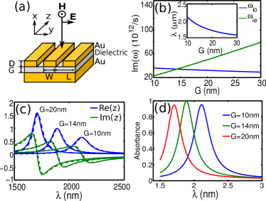
Simple designs of narrow-band MM absorbers (NBMA) comprised of an array of plasmonic strips/patches separated by a thin dielectric spacer from a ground plate, as illustrated in Fig. 1(a), have been recently proposed and experimentally implemented wu_spie08 ; giessen_nl10 ; padilla_apl10 ; wu_2011 . “Perfect” ( at the peak) light absorption by NBMAs is enabled by the resonant excitation of a surface plasmon polariton (SPP) whose frequency is controlled by the structural dimensions. Using such NBMAs as building blocks for a broad-band metamaterial absorber (BBMA) appears straightforward: combining several such blocks () with spectrally-close absorption peaks at and bandwidths into a macro-cell should deliver the desired broad-band feature as long as . In reality, designing BBMAs using this approach padilla_prl11 has been challenging. For example, the individual absorption peaks of the constitutive NBMAs can each yield “perfect” absorption, but at the expense of large spectral separation. Alternatively, constitutive NBMA’s with spectrally-close absorption peaks can fail to provide “perfect” absorption at every peak. Systematic approach to designing NBMAs and combining them into a unit cell of a BBMA is needed. In this Letter, we provide such an approach based on a simple impedance model. We show that the surface impedance of a BBMA can be obtained from the impedances of the constitutive NBMAs using a simple additive formula (see Eq. (3)), which is valid as long as the SPPs’ propagation lengths are much smaller than the separation between NMBAs.

We start by introducing a simple single-resonance model of an NMBA based on the periodic structure shown in Fig. 1(a). The structure coupled to the incident radiation is described within the framework of a single resonator model haus_1984 . An open resonator is defined by its natural frequency, , and finite lifetimes, and , respectively determined by the Ohmic and radiative losses. The interaction between the resonator and the incident field of amplitude is described by the following equations:
| (1) |
where and are the amplitudes of the resonator and the reflected field, respectively. The specific geometry of the resonator that includes the ground plate is manifested in the expression for , which is a superposition of the resonator and ground plate reflection. Within this simple single-resonance model, the surface impedance defined as , where , is given by:
| (2) |
and all optical properties of the NBMA are determined by three parameters: , , and . These parameters depend on the structural dimensions and can be obtained by calculating the “leaky” SPP eigenmodes wu_2011 using eigenvalue simulations (i.e., no incident field). By tuning the geometric parameters of the NBMA, one can engineer , , and and achieve (and, therefore,perfect absorption) whenever the critical coupling condition is satisfied.
The validity of the single-resonance model was verified for several NBMAs as shown in Fig. 1. Plasmonic strips and ground plate are assumed to be made of gold (described by the Drude permittivity , where and ) and the spacer is assumed to have a non-dispersive dielectric permittivity . The accuracy of the obtained from Eq. (2) was verified by comparing it to the impedance obtained from the reflection coefficients calculated at various frequencies of the incident radiation. Excellent agreement shown in Fig. 1(c) validates the single-frequency model which is highly computationally efficient because only a single eigenvalue/eigenmode simulation is required wu_2011 to determine for all frequencies.
The tunability of the NBMA’s frequency characteristics with respect to the spacer thickness is illustrated in Fig. 1(b). Note from Fig. 1(d) that considerable peak absorbances (in excess of ) is achieved for a wide range of spacer thicknesses . The smooth dependence of the frequency characteristics on shown in Fig. 1(b) (as well as on the other structure parameters) enables rapid design of the appropriate parameter set (, , , ) of the NBMA that provides the targeted .
Two important features of the NBMAs described in Fig. 1 make them promising building blocks for designing a BBMA. First, their period is strongly sub-wavelength: . That implies that a sub-wavelength () unit cell of a BBMA can accommodate a large number of NBMA-based sub-units satisfying . Second, the propagation length of the SPP responsible for absorption satisfies . This property has been shown wu_2011 to be related to the wide-angle absorbance of the NBMA. While these two conditions are related, they are not equivalent as shown below. Nevertheless, when both conditions are satisfied, a simple expression for a the surface impedance of a BBMA with a macro-cell composed of NBMA’s can be obtained:
| (3) |
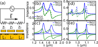
where () is the impedance (period) of each periodic constitutive NBMA. Derivation of Eq. (3), based on the series combination model engheta_07 , is illustrated in Fig. 2(a), where the external field represents a voltage drop and each NBMA resonator is treated as a circuit element. The key assumption is that each component of the circuit functions independently from each other, i.e., there is little mutual capacitive or inductive coupling between adjacent sub-units. This condition is satisfied owing to the second feature of NBMAs. Below we verify Eq. (3) for two cases: (i) strongly (Fig. 2(b,c)) and (ii) weakly (Fig. 2(d,e)) confined SPPs of the individual sub-units. In each case the unit cell of a candidate BBMA consists of two sub-units with dimensions stated in Fig. 2.

In case (i), excellent agreement between BBMA’s impedance calculated from Eq. (3) and from direct numerical simulations is shown in Fig. 2(b). Each sub-unit, representing a resonant high-impedance () surface, is independent of the other inside the macro-cell because . The impedance of the combined candidate BBMA has two spectral peaks with values corresponding to absorption. On the other hand, Eq. (3) clearly fails in case (ii) as shown in Fig. 2(d). That is because , and the two sub-units strongly interact inside the macro-cell, thereby invalidating the series impedance model. Note that to achieve such long propagation length of the SPP, the electron collision frequency, , in Au has been artificially reduced by a factor of four.

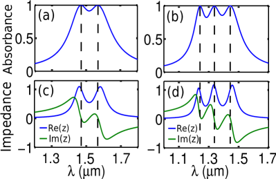
We now present two examples of BBMAs constructed by engineering their unit cells from several (two in Fig. 3(a,c) and three in Fig. 3(b,d)) NBMA sub-units. We use the example of two sub-units inside the unit cell of a BBMA to describe the computational procedure for obtaining an absorber with two absorption peaks at the prescribed frequencies and . That corresponds to , where is calculated from Eq. (3). The resulting four equations (note that is a complex number) must be satisfied for four unknown. For simplicity, we assume and to be fixed. This leaves the complex impedance as a function of four unknowns that can be numerically solved for to satisfy the above four equations. The numerical implementation based on the multi-dimensional Newton’s method is greatly simplified by the variables’ separation in Eq. (3): the number of partial derivatives , is reduced because , where is the impedance of one single sub-unit.
The results of such numerical calculations for a BBMA with two sub-unit per unit cell are shown in Fig. 3 (left column), where the resulting double-peaked impedance is plotted in Fig. 3(c) and the corresponding frequency-broadened absorptivity is plotted in Fig. 3(a). A similar numerical procedure was employed to design a triple-peaked BBMA illustrated in Fig. 3 (right column; all sub-unit parameters in the caption). Note that over absorptivity is achieved over the spectral range of . Note that in both examples presented in Fig. 3 the periodicity of the BBMA is sub-wavelength: . It is essential to satisfy this condition to avoid the emergence of the additional diffraction orders which create additional radiative loss channels and further complicate the impedance model. In practice, this sets a limit on the attainable bandwidth. For example, for the strip-based designs presented in this Letter, the number of sub-units is limited to (or for a patche-based design). A possible solution could involve an aperiodic distribution of sub-units. Based on negligible interaction between the sub-units, it is expected that Eq. (3) should hold.
In conclusion, we have demonstrated that a broad-band metamaterial absorber (BBMA) can be designed by constructing a super-lattice structure with each sub-lattice absorbing at different frequencies. Based on a single oscillator model and a series circuit model, broad-band absorbers with multiple perfectly absorbing peaks are shown to be attainable, and a procedure for designing such absorbers is provided. Examples of BBMAs comprised of two and three sub-units operating in the telecommunications frequency range are presented, and an average absorbance in the range is predicted. Such ultra-thin (nm) BBMAs can be used for infrared detection and other applications. This work is supported by the Office of Naval Research (ONR) grant N00014-10-1-0929.
References
- (1) I. V. Lindell, S. A. Tretyakov, K. I. Nikoskinen, and S. Ilvonen, “BW media-Media with negative parameters, capable of supporting backward waves,” Microw. Opt. Techn. Let., 31, 129-133 (2001).
- (2) D. R. Smith and D. Schurig, “Electromagnetic wave propagation in media with indefinite permittivity and permeability tensors,” Phys. Rev. Lett., 90, 077405 (2003).
- (3) Fei Le, Daniel W. Brandl, Yaroslav A. Urzhumov, Hui Wang, Janardan Kundu, Naomi J. Halas, Javier Aizpurua , and Peter Nordlander, “Metallic nanoparticle arrays: a common substrate for both surface-enhanced Raman scattering and surface-enhanced infrared absorption,” ACS Nano, 2, 707 (2008).
- (4) Paul L. Stiles, Jon A. Dieringer, Nilam C. Shah, and Richard P. Van Duyne, “Surface-enhanced Raman spectroscopy,” Annu. Rev. Anal. Chem, 1, 601 (2008).
- (5) Harry A. Atwater and Albert Polman, “Plasmonics for improved photovoltaic devices,” Nature Materials, 9, 205 (2010).
- (6) R. Adato, A. A. Yanik, J. J. Amsden, D. L. Kaplan, F. G. Omenetto, M. K. Hong, S. Erramilli, and H. Altug, “Ultra-sensitive vibrational spectroscopy of protein monolayers with plasmonic nanoantenna arrays,” Proc. Natl. Acad. Sci. USA, 106, 19227 (2009).
- (7) N. I. Landy, S. Sajuyigbe, J. J. Mock, D. R. Smith, and W. J. Padilla, “Perfect metamaterial absorber,” Phys. Rev. Lett., 100, 207402 (2008).
- (8) C. Wu, Y. Avitzour, and G. Shvets, “Ultra-thin wide-angle perfect absorber for infrared frequencies,” Proc. SPIE, 7029, 70290W (2008).
- (9) Y. Avitzour, Y. A. Urzhumov, and G. Shvets, “Wide-angle infrared absorber based on a negative-index plasmonic metamaterial,” Phys. Rev. B, 79, 045131 (2009).
- (10) Na Liu, Martin Mesch, Thomas Weiss, Mario Hentschel, and Harald Giessen, “Infrared perfect absorber and its application as plasmonic sensor,” Nano Letters, 10, 2342 (2010).
- (11) Jiaming Hao, Jing Wang, Xianliang Liu, Willie J. Padilla, Lei Zhou, and Min Qiu, “High performance optical absorber based on a plasmonic metamaterial,” Appl. Phys. Lett., 96, 251104 (2010).
- (12) Chihhui Wu, Burton Neuner III, Jeremy John, Andrew Milder, Byron Zollars, Steve Savoy, and Gennady Shvets, “Large-area wide-angle spectrally selective plasmonic absorber,” Phys. Rev. B, 84, 075102 (2011).
- (13) Xianliang Liu, Talmage Tyler, Tatiana Starr, Anthony F. Starr, Nan Marie Jokerst, and Willie J. Padilla, “Taming the blackbody with infrared metamaterials as selective thermal emitters,” Phys. Rev. Lett., 107, 045901 (2011).
- (14) Hermann A. Haus, “Waves and fields in optoelectronics,” (Prentice-Hall, 1984).
- (15) Alessandro Salandrino, Andrea Alu, and Nader Engheta, “Parallel, series, and intermediate interconnections of optical nanocircuit elements. 1. Analytical solution,” J. Opt. Soc. Am. B, 24, 3007 (2007).