Modeling and Simulation of a Microstrip-SQUID Amplifier
Abstract
Using a simple lumped-circuit model, we numerically study the dependence of the voltage gain and noise on the amplifier’s parameters. Linear, quasi-linear, and nonlinear regimes are studied. We have shown that the voltage gain of the amplifier cannot exceed a characteristic critical value, which decreases with the increase of the input power. We have also shown that the spectrum of the voltage gain depends significantly on the level of the Johnson noise generated by the SQUID resistors.
I Introduction
A microstrip-SQUID (superconducting quantum interference device) amplifier (MSA) has been designed as a low noise radiofrequency amplifier, which is able to operate above 100 MHz 1 . The MSA has been studied theoretically in many publications 1 ; referee1 ; referee2 ; 2 ; 3 ; 4 ; 5 ; 6 ; 7 . However, a consistent theoretical model of MSA has not yet been developed. The circuit diagram of lumped model of MSA is presented in Fig. 1. This MSA consists of a linear input circuit coupled to the direct current (dc) SQUID via the mutual inductance, . Note that the isolated dc SQUID is a nonlinear circuit, while the isolated microstrip is a linear circuit. The total system consisting of the SQUID and the input circuit is a nonlinear one. Consequently, it remains no trivial task to predict the performance of the MSA during the design process. Therefore analytical investigation and extensive numerical modeling, simulation, and optimization of the MSA are required before creating the device. Generally, the solutions for the MSA model must be obtained by solving analytically or numerically the system of nonlinear ordinary differential equations written for the SQUID coupled to the input circuit. The dynamics of a bare SQUID was investigated numerically in tesche1 ; tesche2 ; tesche3 .

The objective of our paper is to study numerically the dynamics of exact nonlinear equations describing the MSA, and to compute the voltage gain, , of the MSA, where is a Fourier harmonic of the output voltage on the SQUID, and is the amplitude of the input voltage on the microstrip at the same frequency, . We analyze numerically both linear and nonlinear regimes of amplification. A linear regime means that the following linear dependence exists: , where the gain is independent of the . We also simulate the output spectral density of voltage Johnson noise, originated in shunting resistors of the SQUID and the resistor, , in the input circuit, and calculate the noise temperature.
II Input circuit
Consider the isolated linear input circuit (). The forward impedance of the input circuit is
| (1) |
In Fig. 2 we plot the amplitude of the current, , in the input coil with inductance , when . One can see from Fig. 2 that as decreases, the maximum shifts to higher frequencies, and the width of the peak decreases. One can use this latter property to create a narrow-bandwidth amplifier. The frequency corresponding to the maximum is always less than the resonant frequency, , of the input resonator.

III Equations of motion
The differential equations of motion for the SQUID are: 2
| (2) | |||
Here the dot above and indicates time differentiation; is the reduced flux quantum; is Planck’s constant; is the electron charge; and are the phase differences in the Josephson junctions in the SQUID; is the Josephson junction critical current; and describe the noise current (Johnson noise) originating in the shunt resistors, . The output voltage, , can be expressed in terms of the Josephson junction phase differences
In order to determine in the third equation in (III), we have to add the differential equations for the input circuit. The total system of eight first-order differential equations can be written in the following form:
Here
is the charge on the capacitor ; is the charge on the capacitor ; is the frequency of the external voltage; and is the noise voltage on the the resistor ; is the noise current through .
The input circuit is coupled to the SQUID through the term, , in the fourth equation in (III), and the SQUID is coupled to the input circuit by the effective coupling constant, , in the last equation in (III). Since the effective coupling constant, , is proportional to , the effective coupling can be increased by decreasing .
IV Voltage gain
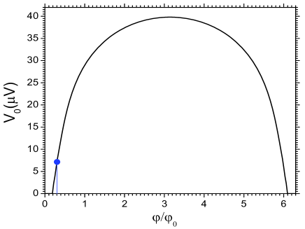
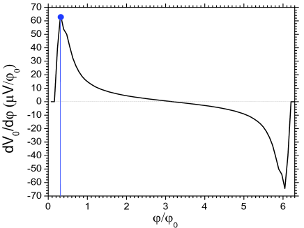
First we choose the optimal working point of our amplifier which is defined by the value of , provided the other parameters are given. In Fig. 3 the time average, , of the output voltage and its derivative (transfer function) are plotted as a function of . The maximum of the transfer function occurs in the vicinity of which we choose as our working point.
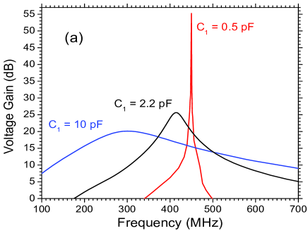
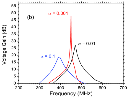
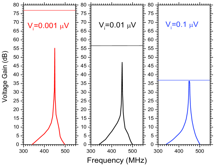
In Fig. 4(a) we plot the voltage gain for three values of the coupling capacitance, . By comparison of Fig. 4(a) with Fig. 2, one can conclude that the amplifier gain is mostly defined by the parameters of the input circuit. The gain of 55 dB for pF is the combined result of amplification by the input circuit and by the SQUID due to the strong interaction between them when is small and positive. Note that the dimensionless parameter, , contains both the parameters of the SQUID () and the input circuit (), as well as the coupling inductance, . In Fig. 4(b) we plot the gain for three values of : , 0.01, and 0.1. The gain decreases from 55 dB to 27 dB as increases from 0.001 to 0.01. The value of coupling inductance, , changes, respectively, from 2.2982 nH to 2.2878 nH, that is, by only 0.44 percent. Therefore, the possibility of obtaining the large gain is limited to a very small region of the parameters. For this purpose it is desirable to have a tunable coupling inductance, , or a tunable input circuit inductance, , or a tunable SQUID inductance, .
Consider the situation in which is negative, that is . In order to understand the dynamics in this regime, we differentiate the last equation in (III) and use the 4th and 7th equations for and . We obtain an equation for the oscillations of the input current, , with an external force and with the eigenfrequency, , where
Negative corresponds to negative real part of the input impedance negative2 ; negative3 . This regime can drive the resonator into instability negative1 .
V Nonlinearity
When the input voltage amplitude or gain becomes sufficiently large, the nonlinear effects in the SQUID become important. In the nonlinear regime, the nonlinear effects decrease the output voltage of the SQUID, thus decreasing the gain of the amplifier in comparison with the linear regime. It is reasonable to assume that the MSA is in the nonlinear regime when the output voltage becomes comparable with the SQUID’s own average output voltage, . It is convenient to define the maximum gain
| (4) |
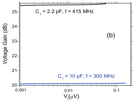
When the amplitude, , of the amplified output Fourier harmonic approaches , the gain should decrease due to nonlinear effects in the SQUID. If, for example, the amplitude of the input signal is V and V (see left side in Fig. 3 for ), according to Eq. (4) the gain is limited by the value . In order to obtain a gain of dB in Figs. 4(a) and (b), we set the amplitude of the input signal to be V. For this input signal expressed in decibels , we have dB, so that . For V, we have dB, and for V one obtains dB. In Fig. 5 we plot the gain, , for three values of . One can see from the figure that is less than for all frequencies, . (The values of for each are indicated in the figures by the horizontal lines.) In Fig. 6(a) we plot as a function of . As follows from the figure, the condition is also satisfied for all input voltage amplitudes, . As the amplitude, , of the input signal increases, both in Eq. (4) and the gain, , decrease. This nonlinear effect cannot be obtained from a linearized theory, like that based on an effective impedance of the amplifier martinis . In Fig. 6(b) the amplifier is in the linear regime for pF and pF because the gain is sufficiently small, .

VI Noise
We assume that the Johnson noise voltages across the resistors dominate all other sources of noise in the amplifier. White Gaussian noise in each of three resistors was modeled by a train of rectangular pulses following each other without interruption. The current amplitude, , of each pulse is random with zero average and the following variance:
Here the brackets indicate an average over different realizations; is the Botzmann constant; is the temperature of the MSA; is the duration of each pulse, which is constant in our simulations; is the corresponding resistance: for the shunting resistors in the SQUID and for the resistor in the input circuit. In Fig. 7 we plot the output voltage spectral density, (where ), when no input voltage is applied to the input circuit, . is defined as:
where is the time of integration of the output signal and the angular brackets, , indicate an average over different realizations.

One can use the voltage spectral density, , to calculate the noise temperature of the amplifier, , using the following equation:
In Fig. 8 we plot , as a function of frequency, , for two different scales, where is the quantum temperature. We use the noise spectral density, , from Fig. 7 and the gain from Fig. 4(a). At the minimum, for pF (red line) the noise temperature is negative.


We now show that this negative noise temperature is related to the method of its calculation. The reason for the negative noise temperatures is in the different methods of calculation of the noise spectral density and the gain of the amplifier. There are three resistors that act as sources of noise: two resistors, , in the SQUID and the resistor, , in the input circuit. All three resistances contribute to the noise spectral density, . The noise current in the SQUID, besides contributing to noise spectral density, changes the SQUID’s parameters, including the frequency at which the gain is maximum. At one moment the SQUID is tuned to one frequency and at the next moment it is tuned to another frequency. The noise voltage generated in the resistor, , is amplified by the detuned SQUID. On the other hand, the signal is amplified by the SQUID tuned to a definite frequency because there are no noise currents in the resistors, , of the SQUID. Consequently the amplification of the signal is greater than the amplification of the noise. Besides, the noisy SQUID shifts the frequency at which the amplification is maximum. In Fig. 4(a) the maximum is at MHz, while in Fig. 7 the maximum is at MHz.


By this argument, we calculated the gain (Fig. 9) and the noise temperature (Fig. 10) with noise on the resistors, , and with the input signal, . The calculated gain in Fig. 9 is qualitatively similar to that measured experimentally in Ref. kinion . If the time of integration is sufficiently long, the contribution of the noise to the gain is minimized, so only the contribution from the amplified signal remains (see Fig. 11). In this situation both the voltage spectral density and the gain are calculated for the same system with the noisy (detuned) SQUID. Note that a significant asymmetry of the spectrum for pF and 10 pF in Figs. 8 and 10 appears because we plot the ratio , where the quantum temperature is proportional to the frequency .
We demonstrated two methods of calculating gain and noise temperature of the MSA. The noise on the shunting resistors of the SQUID reduces gain of the amplifier if one compares Figs. 4(a) (no noise) with Fig. 9 (with noise). The reduction is large for small capacitance, pF, while the gain for pF is mostly not affected by the noise in the SQUID. The gain calculated in the previous sections of this paper is actually the gain at zero temperature.
In summary, we have simulated the dynamics of the microstrip-SQUID amplifier in both the linear and nonlinear regimes and studied the dependence of the voltage gain and noise on the parameters of the amplifier. We have shown that the voltage gain cannot exceed the critical value given by the formula (4). This value is inversely proportional to the input voltage. It is shown that the gain decreases as the device temperature increases. Finally, we have shown that the spectrum of the voltage gain depends significantly on the level of the Johnson noise in the SQUID resistors. This effect must be taken into account for correct calculation of the amplifier noise temperature. The next important step should be the optimization of the gain and noise temperature with respect to the amplifier’s parameters.
Acknowledgements
This work was carried out under the auspices of the National Nuclear Security Administration of the U.S. Department of Energy at Los Alamos National Laboratory under Contract No. DE-AC52-06NA25396 and by Lawrence Livermore National Laboratory under Contract DE-AC52- 07NA27344. This research was funded by the Office of the Director of National Intelligence (ODNI), Intelligence Advanced Research Projects Activity (IARPA). All statements of fact, opinion or conclusions contained herein are those of the authors and should not be construed as representing the official views or policies of IARPA, the ODNI, or the U.S. Government.
References
- (1) J. Clarke, M. Hatridge, and M. Mossle, Annu. Rev. Biomed. Eng. 9, 389 (2007).
- (2) M. Mück and R. McDermott, Supercond. Sci. Technol., 23, 093001 (2010).
- (3) M. Mück and J. Clarke, J. Appl. Phys., 88, 6910 (2000).
- (4) J. Clarke, T. L. Robertson, B. L. T. Plourde, A. Gacsia-Martines, P. A. Reichardt, D. J. Van Harlingen, B. Chesca, R. Kleiner, Y. Makhlin, G. Shon, A. Shnirman, and F. K. Wilhelm, Phys. Scripta 102, 173 (2002).
- (5) B. L. T. Plourde, T. L. Robertson, P. A. Reichardt, T. Hime, S. Linzen, C.-E. Wu, and J. Clarke, Phys. Rev. B 72, 060506 (2005).
- (6) M. Hamalainen, R. Hari, R. J. Ilmoniemi, J. Knuutila, and O. V. Lounasmaa, Rev. Mod. Phys. 65, No. 2, 413 (1993).
- (7) R. Bradley, J. Clarke, D. Kinion, S. Matsuki, M. Muck, and P. Sikivie, Rev. Mod. Phys, 75, 777 (2003).
- (8) S. Michotte, Appl. Phys. Lett. 94, 122512 (2009).
- (9) M. Mück, J. B. Kycia, and J. Clarke, Appl. Phys. Lett. 78, 967 (2001).
- (10) C. D. Tesche, and J. Clarke, IEEE Transactions on Magnetics, v. MAG-13, No. 1, 859 (1977).
- (11) C. D. Tesche, and J. Clarke, J. Low Temp. Phys., 29, 301 (1977).
- (12) C. D. Tesche J. Low Temp. Phys., 44, 119 (1981).
- (13) C. Hilbert and J. Clarke, J. Low Temp. Phys., 61, 237 (1985).
- (14) P. Falferi, R. Mezzena, S. Vitale, M. Cerdonio, Appl. Phys. Lett. 71, 965 (1997).
- (15) A. Vinante, M. Bonaldi, P. Falferi, M. Cerdonio, R. Mezzena, G. A. Prodi, and S. Vitale, Physica C, 368, 176 (2002).
- (16) J. M. Martinis and J. Clarke, J. Low Temp. Phys., 61, 227 (1985).
- (17) D. Kinion and J. Clarke, Appl. Phys. Lett., 92, 172503 (2008).