Ironsilicide formation by high temperature codeposition of Fe-2Si with different thicknesses on Si (111)
Abstract
Fe and 2Si were co-deposited on Si (111) surface at 853 K. The formation of silicides was investigated by M ossbauer spectroscopy and electron microscopy. Depending on the thickness of the deposited films different phases were formed. At low thickness, stable -FeSi (B20) and metastable [CsCl]-Fe1-xSi (B2) phases were observed. In the latter case, because of the presence of Fe vacancies in the lattice the local symmetry around the iron components was lower than cubic. At larger (12 nm) deposited thickness, stable -FeSi2 has been formed.
keywords:
Interface structure, Microscopy of films, Phase identificationPACS:
61.35.Ct, 68.37.-d, 68.55.Nq1 Introduction
The formation of iron silicide phases on silicon substrate attracted
considerable attention in the last decades
[1, 2, 3, 4, 5, 6]. The
particular aim was to determine the Fe-silicide structures and
possibly to grow epitaxial semiconducting -FeSi2 layers
on/in Si, since -FeSi2 has a direct gap of 0.87 eV, and
could be used in optoelectronic device fabrication. However, the
formation of iron-silicides proved complex processes, especially, depending on
the preparation methods. The interface formation involves reactive
intermixing between iron and silicon at the deposition process and
the resulting Fe-silicide forms on the surface of the Si substrate.
First, Fe depositions were made at room temperature, later on
heated Si substrate [7]. In order to decrease possibly the
out diffusion of the substrate Si atoms during the formation of the
Fe-silicide phases on the surface, the films were grown by co-depositing Fe and Si in different [8, 9] concentration ratio (1:1, 1:2). The
experiments resulted in various iron silicide phases. The phases crystallized in cubic structure [8, 10] and in non-stoichiometric composition. The structure and morphology aspect of the Fe-silicide was investigated [11] by X-ray diffraction (XRD) and reflective high energy electron diffraction (RHEED) methods during the co-deposition of Fe and Si in 1:2 ratio on Si(111) during
different deposition times at 580∘C. It was observed that during the growth process, first separate then intergraded islands (in layer form) were formed. The RHEED images were observed during the depositions at low thickness and the images were interpreted by the formation of -FeSi2. At thicker depositions, the -FeSi2 phase was observed.
In order to gain more information on the Fe-silicide phases forming at different thicknesses we performed Mössbauer and electron spectroscopy
studies on the co-deposited Fe-2Si samples in order to get correct information
on the different Fe-silicide phases, especially, on the formation of the -FeSi2 phase. The Mössbauer effect
using conversion electron spectroscopy (CEMS) is a very sensitive
method to observe correct phase formation on surfaces between iron and silicon.
The electron microscopy, especially, in transition electron microscopy (TEM) mode is very effective for structural determination of the phases. The parallel application of the two methods may provide reliable results on the formation of different phases depending on the different thicknesses.
2 Experimental Details
High purity Si (111) substrates were chemically etched in an aqueous
solution containing 10 mol. percent HF and 40 mol. percent NH4F
to get rid of the oxide on the surface. In a pre-annealing chamber
( 1 x 10⁻¹⁰ mbar), the samples were introduced and heated
to 875 K for 30 min. After this treatment, the Si substrates were
transported into the chamber of an MBE (MECA) system. Fe
and Si atoms were co-deposited with 0.052 : 0.177 volume ratio at 853
K, in 1Fe : 2Si atomic ratio. The base pressure in the chambers was
1x10⁻¹⁰ mbar and increased to 2x10⁻⁹ mbar during the
depositions. 57Fe was evaporated by using Knudsen-cell with BeO
crucible. Si was evaporated by electron gun. The deposition rate was
0.117 Å/sec. Four layers of FeSi2 with 12, 5, 2.5 and 1,3 nm
thicknesses were prepared.
Mössbauer measurements were carried out by using a conventional
constant acceleration-type spectrometer. For the detection of the
conversion electrons a low-background proportional counter filled
with He and 4 vol. percent of CH4 was used at room temperature.
For the analysis of the spectra, a least-squares fitting program was
used. Also, using this program, spectra with histogram distributions
of the parameter values could be fitted. The isomer shift values are
given relative to that of -Fe at room temperature.
Specimens for in-plane electro-microscopic measurements were thinned
by ion milling of the back side. The incidence angle of the iron
beam was 3-5∘ as measured from the surface plan of the
specimen. The conventional TEM investigation of the specimens was
carried out in a PHILIPS CM20 transmission electron microscope
equipped with an EDX analyzer. The high resolution TEM investigation
was carried out in a 300 kV JEOL 3010 TEM and an attached GATAN
TRIDIEM Image FILTER was used for elemental mapping.
3 Results
The Mössbauer spectra of the samples measured at room temperature are shown in Fig. 1.

Quadrupole split spectra were observed for all samples with 12, 5, 2.5 and 1.3 nm thickness values. In the spectrum of 12 nm thick sample (Fig. 1a), two quadrupole split doublet spectra of Lorentian shape could be fitted with the hyperfine parameter values characteristic to the -FeSi2 phase [12]. Spectra of 5, 2.5 and 1.3 nm thick samples showing broad quadrupole split spectra were fitted by parameter distributions because their shapes were not Lorentzian and considerably broadened. The fixed parameters of -FeSi phase were also included (see later). The average isomer shift (), average quadrupole spliting (QS) values are compiled in Table I.
| Thickness nm | Component | QS | W | R. int | |
|---|---|---|---|---|---|
| 12 | 1 | 0.08(2) | 0.56(2) | 0.24(1) | 50(2) |
| 2 | 0.10(2) | -0.34(1) | 0.24(1) | 51(2) | |
| 5 | 1 | 0.18 | 0.66 | 0.26 | 9.2(2) |
| 2 | 0.28 | 0.67 | 0.26 | 90.8(2) | |
| 2.5 | 1 | 0.18 | 0.66 | 0.26 | 11.2(2) |
| 2 | 0.21 | 0.64 | 0.26 | 11.2 (2) | |
| 1.3 | 1 | 0.18 | 0.66 | 0.26 | 13.5(3) |
| 2 | 0.21 | 0.61 | 0.26 | 86.5(1) |
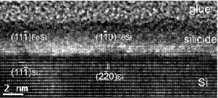
The structure of the 12 and 5 nm thick samples has been investigated by transmission electron microscopy and selected area electron diffraction (SAED) in details both on plane view and cross sectional specimens.
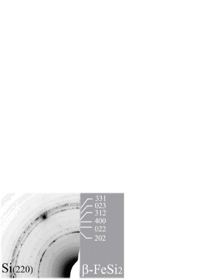
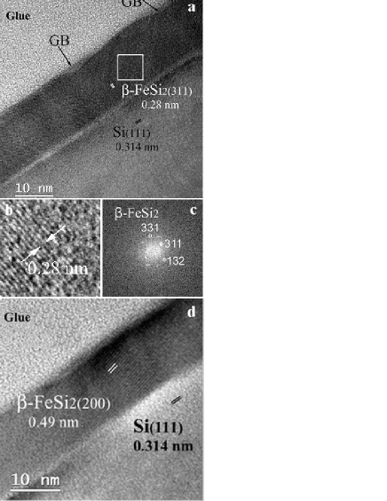
The SAED pattern clearly show that the -FeSi2 crystals are randomly oriented and no epitaxial growth existed. Cross sectional TEM images of the 12 nm sample (Fig. 3) clearly show that the Fe-Si layer is continuous and polycrystalline. In Fig. 3a, b and c -FeSi2 (311) (0.28 nm) lattice fringes are shown. Grain boundaries are shown by arrows in Fig. 3a.
The plain-view bright field (BF) TEM image and the corresponding elemental Fe EELS map of the 5 nm thick sample are shown in Fig. 4a and b.
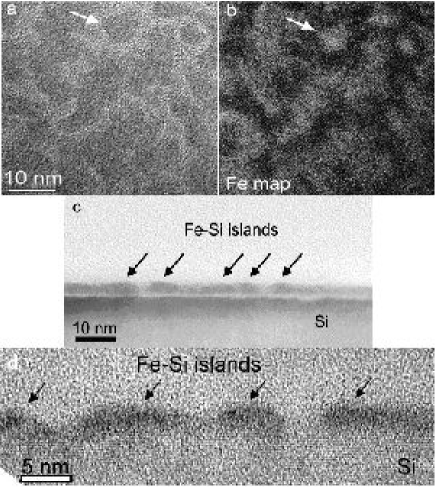
These images clearly show the island structure of the film on the Si (111) substrate. The corresponding TEM BF image and EELS elemental map represent the same area (one of islands is marked by arrows on both images). In the bright field image, the Fe/Si islands show dark contrast due to the higher atomic number of Fe, while in the Fe elemental EELS map the Fe/Si islands are shown as bright contrast. Fig.4c and d demonstrate also the domain structure of the Fe la-Si layer in cross section. The SAED analysis of the crystal structure is shown in Fig.5.
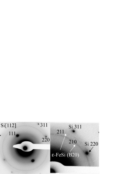
In this diffraction pattern only the -FeSi (B2) [ JCPDS 76-1748 ] phase can be identified. Cross sectional TEM images of the 5 nm thick sample is shown in Fig. 6.
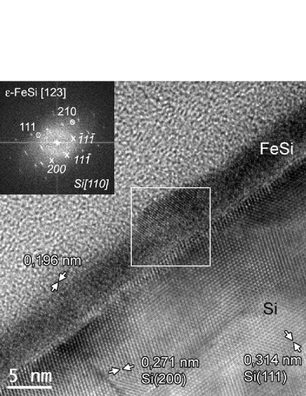
Lattice spacings of 0.190-0.199 nm as single set of lattices have been found in several islands. These could belong to the (210) lattice planes (0. 199 nm) of the -FeSi identified by the SAED analysis of the plane view specimen. In Fig. 7, the high resolution TEM image is shown in the Si [112] direction.
The layer is grown epitaxially on the Si substrate surface and it could be identified as [CsCl]-Fe1-xSi (B2) [JCPDS26-1141]. The spectra of the thinner deposits showed thinner and smaller islands but the same images as the 5 nm thick sample.
4 Discussion
The HRTEM and SAED as well as FFT and Mössbauer analysis of the
12 nm thick Fe-Si sample proved the formation of -FeSi2 in
the co-deposited layer. The film was continuous with randomly
oriented grains corresponding to the structure evolution of the
poly-crystalline film. The -FeSi2 phase formed because of
the relatively large formation heat and the lower effect of the Si substrate surface potential for the thicker layer. No other phases could be detected.
The structural results of the thinner layers appeared more complex.
The morphological evolution during the thin film growth is
a complex process resulting from the inhibition on the time-scale
of deposition and to reach an equilibrium state. The depletion zones
can have different dimensions depending on the substrate structure
and the surface energy values. The high temperature mainly results
in local rearrangement of the atoms, not in long range diffusion or
inducing chemical reaction with surface atoms
as it is in the case of reactive deposition to the surface of a substrate.
The formation of phases depend also on the
heat of formation of the different phases [14, 15].
Concerning the Si - Fe phases, the -FeSi has the maximum
heat formation value calculated in [16].
-FeSi has cubic structure but the Mössbauer
spectrum of -FeSi shows quadrupole split spectrum
because of the lower than cubic symmetry in the nearest neighborhood
of the Fe in the lattice. This doublet may overlap with the other doublet
component(s) in the broadened spectrum of 5 nm and in the thinner samples. The broad spectrum could be fitted by fixing the known hyperfine parameter
values [17]. For -FeSi, 9(2) percent relative
intensity value was obtained for the 5 nm thick sample. The relative
intensities for this phase are somewhat larger in thinner samples. Since the spectra are overlapped with the broad spectrum the exact real line width of the -FeSi component can not be exactly known and this may effect the relative intensity of this component. The broad quadrupole doublet can be interpreted by the formation of disordered
[CsCl]-Fe1-xSi as it is mentioned in Results caption. The formation of [CsCl]-Fe1-xSi can be the result of the stabilization of the Fe-Si positions by forming epitaxial
structure on the Si surface and in the positions where small
Si crystal is present in the deposited layer. The high resolution TEM image shows
that the [CsCl]-Fe1-xSi (B2) phase is present
in the domain islands on the Si surface. This phase was also observed
after laser treatment of -FeSi layer on Si substrate
[18]. The hyperfine interaction values of the thin layers having parameter distributions (Table I.) and are in the range of the values published by the referred authors.
The illustration of the Fe1-xSi lattice with Fe vacancies is shown in Fig. 8.
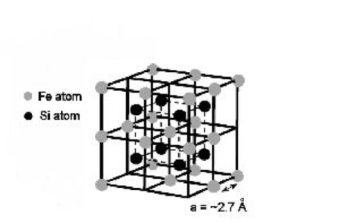
The structure of the -FeSi2 phase has cubic fluorite-type structure [20]. This case, the Mössbauer spectrum should appear as a single line. But such component did not appear in our spectra in agrement with the measured TEM image. The reason is that the structure contains Fe vacancies positioned not regularly resulting in electric field gradient at the Fe sites, consequently, quadrupole split M ssbauer spectra with the distribution of the parameter values. At higher deposited thickness of Fe-2Si, -FeSi and [CsCl]-Fe1-xSi phases do not form.
5 Conclusions
The formation of different phases are determined after co-deposited Fe-2Si on Si (111). It is clearly shown that the formation of phases depends on the thickness of the co-deposited layer on the surface at 853 K. At relatively low deposited thickness two phases form. One is the -FeSi stable phase. The other is [CsCl]-Fe1-xSi with the hyperfine parameter values characteristic to a disordered arrangement around the lattice sites of Fe. The metastable -FeSi2 phase did not form in relatively thin samples. In the 12 nm thick sample, pure stable poly-crystalline -FeSi2 has been formed.
6 Acknowledgement
This work was supported by the Hungarian National Research Fund (OTKA) project No. K62272 .
References
- [1] C. Calandra, O. Bisi and Ottaviani, Surf. Sci. Rep. 4 (1981) 271 and references therein
- [2] S. P. Murarka, Silicides for VLSI Applications (Academic Press, New York, 1985)
- [3] M. C. Bost and J. E. Mahan, J. Appl. Phys. 64 (1988) 2034
- [4] J. Desimoni and F. H. Sanchez, Hyp. Int. 122(1999) 277
- [5] V. E. Borisenko, Semiconducting Silicides (Springer-Verlag, Berlin, 2000)and references therein
- [6] C. M. Comre, A. Falepin, O.Richard, H. Bender, and A. Vantomme, J.Appl.Phys.95 (2004) 2365
- [7] J. Derien, J Chevrier, V. Le Thanh and J. Mahan, Appl. Surf. Sci. 56/58 (1992) 382; J. Derien, J. Chevrier, V. Le Thanh,T. E. Crumbaker, J. Y. Natoni and I. Berbezier, Appl. Surf. Sci. 70/71 (1993) 546
- [8] H. von Känel, N. Onda, H. Sirringhaus, E. Müller-Gubler, S. Concalves-Conand C. Schwarz, Appl. Surf. Sci. 70/71 (1993) 5559
- [9] L. Wang, C. Lin, G. Shen, X. Lin, R. Ni and S. Zou, Appl. Phys. Lett. 66 (1995) 3453
- [10] N. Onda, J. Henz, E. Müller, K. A. Mäder and H. von Känel, Appl. Surf. Sci. 56-58 (1992) 426
- [11] S. Y. Ji, J. F. Wang, J. W Lim and M. Isshiki, Appl. Surf. Sci. 253 (2005) 444
- [12] M. Fanciulli, C. Rosenblad, G. Weyer, A. Svane, N. E. Christensen and H. J. von Känel, Phys. Rev. Lett. 75 (1995)1642
- [13] S. Walter, R. Bandorf, W. Weiss, K. Heinz, U. Starke, M. Strass, M. Bockstedte, and O. Pankratov, Phys. Rev. B 67 (2003) 085413
- [14] R. Pretorius, T. K. Marais and C. C. Theron, Mat. Sci. and Engineering 10 (1993) 1
- [15] R. Peretorius, C. C. Theron, A. Vantomme and J. W. Mayer, Crit. Rev. in Solid State and Materials Science, 24 (1999) 1
- [16] A. R. Miedema, P. F. deChatel and F. R. deBoer, Physica 100B (1980) 1
- [17] M. Fanciulli, A. Zenkevich, I. I. Wenneker, A. Svane, N. E. Christensen and G. Weyer, Phys. Rev. B 54 (1996) 15985
- [18] A. Falepin, S. Cottenier, C. M. Comrie and A. Vantomme, Phys. Rev. B 74 (2006) 184108
- [19] J. Desimoni, F. H. Sanchez, M. B. Fernández van Raap, H. Bernas, C. Clerc and X. W. Lin, Phys. Rev. B 51 (1995) 86
- [20] J. Derien, I. Berbezier, A. Ronda and J. Y. Natoli, Appl. Surf. Sci. 92 (1996) 311