Defect detection in nano-scale transistors based on radio-frequency reflectometry
Abstract
Radio-frequency reflectometry in silicon single-electron transistors (SETs) is presented. At low temperatures (4 K), in addition to the expected Coulomb blockade features associated with charging of the SET dot, quasi-periodic oscillations are observed that persist in the fully depleted regime where the SET dot is completely empty. A model, confirmed by simulations, indicates that these oscillations originate from charging of an unintended floating gate located in the heavily doped polycrystalline silicon gate stack. The technique used in this experiment can be applied for detailed spectroscopy of various charge defects in nanoscale SETs and field effect transistors.
single-electron transistors (SETs) are the most sensitive charge detector available Likharev (1988). Using a SET in a tank circuit resonating at radio frequencies (RF-SET) Schoelkopf et al. (1998), it is possible to reduce system noise by moving away from the background noise and thus achieve a sensitivity approaching [Brenning et al., 2006]. In addition, the aggressive downscaling of silicon technology makes it possible to fabricate Si SETs Guo et al. (1997); Ono et al. (2000); Hofheinz et al. (2006a) and Si RF-SETs Angus et al. (2008) thus achieving the goal of mass production of SETs operating at elevated temperatures Shin et al. (2010). Perhaps the most serious stumbling block on the way to large scale SET integration is the problem of random background charge that unpredictably shifts the thresholds of individual devices. At the same time the SET’s innate ability to react to nearby defects and imperfections can be leveraged to develop it into a powerful tool for studies of charged defects, traps and other localized states near the SET. Experimental results reported to date have probed the impact of fluctuators on the low frequency (LF) conduction Hofheinz et al. (2006b); Pierre et al. (2009); George et al. (2010); Golovach et al. (2011) or noise Kafanov et al. (2008) through the SET. In this letter we report on measurements of charged defects in silicon-on-insulator (SOI) SETs using RF reflectometry.
 |

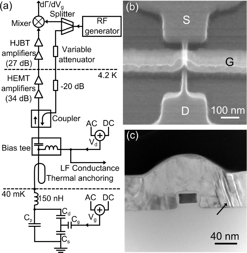
In this work we use a homodyne-detector based RF reflectometry setup (Fig. 1a) similar to that described in Ref. Tang et al., 2009. The sample is embedded in a resonant circuit consisting of a =150 nH inductor and a parasitic capacitance =0.29 pF. The sample and resonant circuit are mounted on the mixing chamber of a dilution refrigerator, while the bias tee, directional coupler and cold preamplifier are immersed in the helium bath. A change in the device impedance produces a change in the reflection coefficient, , where =50 is the characteristic impedance of the transmission line. The RF test signal, with magnitude 40 V at f=760 MHz, was applied to the tank circuit. To increase the sensitivity of the setup and to suppress a monotonic component of , the derivative was measured. A 20 V modulation signal, at a frequency of =94 kHz, was applied to the gate in addition to the ramp voltage . The reflected signal was amplified, downconverted using a mixer and finally demodulated using a lock-in to produce , as in Ref. Tang et al., 2007; hereafter we refer to this as the RF measurement. For comparison the derivative of the differential conductance was measured with respect to (i.e. ). For this case a 20 V gate modulation was used at a frequency of =8 Hz. The signal, proportional to at a carrier frequency of =278 Hz, was downconverted by a first lock-in and then demodulated by a second lock-in to produce ; we refer to this as the LF measurement.
The devices studied in this article were thin SOI nanowire transistors fabricated on 200 mm wafers in an industrial foundry with a similar design to those in Ref. Hofheinz et al., 2006a, but with either heavily doped polycrystalline silicon (poly-Si) or silicided (NiSi) gates. Figs. 1b and 1c show a top view and transmission electron micrographs (TEM) of one such transistor. At T15 K the devices behave as SETs Hofheinz et al. (2006a) and all devices with poly-Si gates revealed very similar features. The device presented in detail here features a poly-Si gate with a length of 60 nm, a 5 nm SiO2 gate oxide, a channel width of 10 nm and a height of 20 nm.
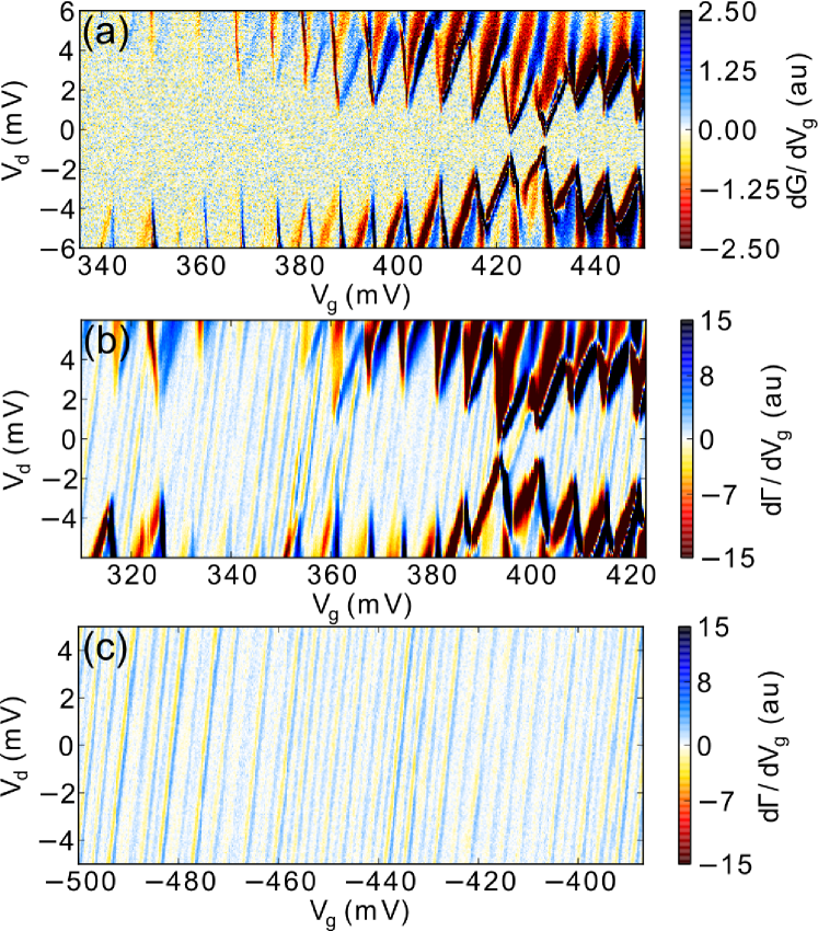
Fig. 2a shows a false-color map of as a function of both and . Figs. 2b and 2c show results of the measurement. Figs. 2b covers the same and range as Fig. 2a. At first glance Fig. 2a and 2b, corresponding respectively to LF and RF measurements, are very similar. The period of Coulomb blockade oscillations and the charging energy fluctuates significantly throughout the charging diagram due to the electrostatic environment of the SET Hofheinz et al. (2006b). In the blockaded (and thus non-conducting) region the results are distinctly different. While no signal can be seen within the Coulomb diamonds of Fig. 2a recorded at LF, in Fig. 2b recorded at RF a large number of quasi-periodic lines are clearly visible. The typical spacing between the lines is close to 2 mV for all the poly-Si gated samples investigated. Change of the resonant frequency did not affect the observation of lines and they disappear due to thermal smearing above 3.5 K. The amplitude of the observed oscillations in is usually two to three orders of magnitude smaller than the features related to the Coulomb diamonds. The consistency of the quasi-period is emphasized in Fig. 2c where a large region of is shown. Note that in this regime the SET is fully depleted and no DC transport occurs. Therefore, the presence of lines in this region of the - map suggests that their origin is extrinsic to the SET itself. The slope is very close to 2 for all of the devices tested with poly-Si gates. This slope is initially surprising as a slope higher than 1 violates the basic model of a charge trap tunnel coupled to the SET island or/and source or drain electrodes. Devices with the same electrode geometry but with a silicided gate were also tested. For silicide the room temperature series resistance of the gate electrode is 2 orders of magnitude lower than that of poly-Si gates; no such lines of slope 2 were observed in these devices.
 |
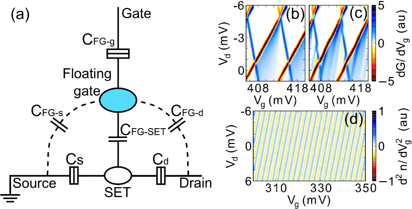
We have concluded that the observed quasi-periodic oscillations are related to charging effects in the poly-Si gate. Indeed, twins and grain boundaries, such as those observed in TEM images (Fig. 1c), which traverse the whole poly-Si film in the region where the gate overlaps the wire can form a “weak link”. At low temperatures they act as tunnel barriers, resulting in a portion of the gate being isolated from the gate electrode. Thus, the part of the gate overlapping the channel becomes an unintended “floating gate” (FG). If the total capacitance of the FG is small enough so that , the charging of the FG is governed by Coulomb blockade. We model the single-electron charging in the system consisting of the SET and FG (the equivalent circuit is shown in Fig. 3a) by voltages applied to the terminals of the SET ( and ) using the master equation technique Bonet et al. (2002) (further details can be found elsewhere Pierre et al. (2009)). The values of 8 aF and 23 aF provide close agreement with the observed period of Coulomb blockade oscillations (=6.7 mV), and typical charging energy (4 meV) of the SET (Fig. 2a). The value of 200 aF was chosen to match the charging energy of the floating gate. From geometric considerations we conclude that the FG is equally coupled to the source and the drain of the SET; the values of 30 aF were then chosen to provide a similar period to the line spacing in Figs. 2b and 2c. In Figs. 3b and 3c a small region of is shown which has been simulated with and without the single-electron charging of the floating gate, respectively, for an estimated electron temperature of 300 mK. The magnitude of the FG charging effect is very small compared with features related to SET charging (Coulomb diamonds), in agreement with the LF measurement shown in Fig. 2a where it is barely visible. However, if the bias across the FG junction lifts the Coulomb blockade, the associated charge transfer results in an increase of the damping of the tank circuit. Therefore the magnitude of the reflected signal changes, resulting in a small but measurable signal as was recently demonstrated by Persson et al. for the detection of a single-electron box chargingPersson et al. (2010). Like in the case discussed in Ref. Persson et al., 2010 the Sisyphus resistance may enhance the observed effect making it possible to detect. We then calculated the population of the FG for changing and , this time for a fully depleted SET (i.e. for the case when the SET island has no extra electrons on it and its population does not change). The change in is expected to be sensitive to . Therefore the second derivative, , was compared to the measured . The simulated oscillation pattern plotted in Fig. 3d closely resembles the measured oscillations shown in Fig. 2b and 2c. To understand the reason for the observed value of the slope 2 for all samples measured we need to look at how the FG charges under the influence of and . Single electron transfers between the FG and the conducting part of the gate are induced by changing potentials at the gate and drain. The period of the single-electron charging in the FG is defined by the total non-leaky capacitor network between FG and source and FG and drain, i.e and . Then, for arbitrary and the slope is given by , and for a slope of 2 is obtained. Likewise, the lines for which cannot be attributed to single electron charging of the FG, but more likely caused by traps tunnel coupled to the SET island or/and source or drain electrodes.
In summary, we report the detection by RF reflectometry of single electron charging in a FG located within the poly-Si gate of a SET. The effect of the FG charging can be avoided by using a silicided gate stack. This is consistent with the industry practice of using silicided or metallic gates instead of poly-Si in RF transistors that operate at room temperature. The RF reflectometry technique may be useful for defect characterization in nanoscale transistors and for characterizing charge-related effects in microelectronics such as advanced gate stacks using high dielectric materials which suffer from granularity and offset charges that can result in large device variability Weber et al. (2008).
We thank R. Wacquez, M. Vinet and B. Previtali from CEA/LETI for sample fabrication. A. O. acknowledges support from SPSMS in CEA-Grenoble, and the university Joseph Fourier in Grenoble. The research leading to these results has received funding from the European Community’s seventh Framework (FP7 2007/2013) under the Grant Agreement Nr:214989. The samples subject of this work have been designed and made by the AFSID project partners http://www.afsid.eu.
References
- Likharev (1988) K. K. Likharev, IBM Journal of Research and Development 32, 144 (1988).
- Schoelkopf et al. (1998) R. J. Schoelkopf, P. Wahlgren, A. A. Kozhevnikov, P. Delsing, and D. E. Prober, Science 280, 1238 (1998).
- Brenning et al. (2006) H. Brenning, S. Kafanov, T. Duty, S. Kubatkin, and P. Delsing, J. Appl. Phys. 100, 114321 (2006).
- Guo et al. (1997) L. Guo, E. Leobandung, and S. Y. Chou, Science 275, 649 (1997).
- Ono et al. (2000) Y. Ono, Y. Takahashi, K. Yamazaki, M. Nagase, H. Namatsu, K. Kurihara, and K. Murase, Appl. Phys. Lett 76, 3121 (2000).
- Hofheinz et al. (2006a) M. Hofheinz, X. Jehl, M. Sanquer, G. Molas, M. Vinet, and S. Deleonibus, Appl. Phys. Lett. 89, 143504 (2006a).
- Angus et al. (2008) S. J. Angus, A. J. Ferguson, A. S. Dzurak, and R. G. Clark, Appl. Phys. Lett. 92, 112103 (2008).
- Shin et al. (2010) S. J. Shin, C. S. Jung, B. J. Park, T. K. Yoon, J. J. Lee, S. J. Kim, J. B. Choi, Y. Takahashi, and D. G. Hasko, Appl. Phys. Lett 97, 103101 (2010).
- Hofheinz et al. (2006b) M. Hofheinz, X. Jehl, M. Sanquer, G. Molas, M. Vinet, and S. Deleonibus, Eur. Phys. J. B 54, 299 (2006b).
- Pierre et al. (2009) M. Pierre, M. Hofheinz, X. Jehl, M. Sanquer, G. Molas, M. Vinet, and S. Deleonibus, Eur. Phys. J. B 70, 475 (2009).
- Golovach et al. (2011) V. N. Golovach, X. Jehl, M. Houzet, M. Pierre, B. Roche, M. Sanquer, and L. I. Glazman, Phys. Rev. B 83, 075401 (2011).
- George et al. (2010) H. C. George, M. Pierre, X. Jehl, A. O. Orlov, M. Sanquer, and G. L. Snider, Appl. Phys. Lett. 96, 042114 (2010).
- Kafanov et al. (2008) S. Kafanov, H. Brenning, T. Duty, and P. Delsing, Phys. Rev. B 78, 125411 (2008).
- Tang et al. (2009) Y. Tang, A. O. Orlov, G. L. Snider, and P. J. Fay, Appl. Phys. Lett. 95, 193109 (2009).
- Tang et al. (2007) Y. Tang, I. Amlani, A. O. Orlov, G. L. Snider, and P. J. Fay, Nanotechnology 18, 445203 (2007).
- Bonet et al. (2002) E. Bonet, M. M. Deshmukh, and D. Ralph, Phys. Rev. B 65, 45317 (2002).
- Persson et al. (2010) F. Persson, C. Wilson, M. Sandberg, G. Johansson, and P. Delsing, Nano Lett. 10, 953 (2010).
- Weber et al. (2008) O. Weber, O. Faynot, F. Andrieu, C. Buj-Dufournet, F. Allain, P. Scheiblin, J. Foucher, N. Daval, D. Lafond, and L. Tosti, in IEDM Tech. Dig. (IEEE, 2008), pp. 1–4.