Signature of Majorana Fermions in Charge Transport in Semiconductor Nanowires
Abstract
We investigate the charge transport in a semiconductor nanowire that is subject to a perpendicular magnetic field and in partial contact with an s-wave superconductor. We find that Majorana fermions, existing at the interface between superconducting and normal sections of the nanowire within certain parameter region, can induce resonant Andreev reflection of electrons at the interface, which yields a zero energy peak in the electrical conductance of the nanowire. The width of the zero energy conductance peak for different experimental parameters is characterized. While the zero energy peak provides a signature for Majorana fermions in one dimensional nanowires, it disappears in a two-dimensional semiconductor thin film with the same experimental setup because of the existence of other edge states in two dimensions. The proposed charge transport experiment may provide a simple and experimentally feasible method for the detection of Majorana fermions in semiconductor nanowires.
pacs:
74.45.+c, 73.63.Nm, 03.67.LxI Introduction
Majorana fermions are quantum particles which are their own anti-particlesMajorana , unlike ordinary Dirac fermions where electrons and positrons (holes) are distinct. Recently, some exotic ordered states in condensed matter systems such as the Pfaffian states in fractional quantum Hall (FQH) systemsFQH1 ; FQH2 ; FQH3 ; FQH4 , chiral p-wave superconductors such as strontium ruthenateIvanov ; SR ; Stone , chiral p-wave fermionic superfluids from p-wave Feshbach resonanceMelo ; Gurarie ; Yip ; Tewari2007 , surface of a 3D strong topological insulator (TI)Fu1 ; Fu2 ; Akhmerov ; Nagaosa1 , as well as semiconductor/superconductor heterostructures have been proposed as platforms supporting Majorana fermionsSau1 ; Sau2 ; Alicea ; Roman1 ; Oreg ; Roman2 ; Mao1 ; Mao2 ; Mao3 . The commonality between these systems is that they all allow quasiparticle excitations which involve no energy cost (the quasiparticle energy is exactly at the Fermi energy). The second quantized operators, , of these zero-energy excitations are self-hermitian, , which is the defining property of Majorana fermions. Essentially this self-hermitian property of Majorana fermions leads to a very non-trivial exchange statistics of these particles called non-Abelian statisticskitaev ; Nayak . Although the emergence of Majorana excitations in low-temperature physical systems would by itself be a truly extraordinary phenomenon, they have also sparked tremendous recent interest because of their potential use in fault tolerant topological quantum computation (TQC)kitaev ; Nayak .
Despite the theoretical success, Majorana fermions have proven to be hard to observe in natural physical systems, such as chiral p-wave superconductors/superfluidsSR ; Tewari2007 . To circumvent this problem, it has been proposed that Majorana fermions may be realized in much more physically robust s-wave superconductors/superfluids by utilizing two additional components: Rashba spin-orbit coupling and Zeeman fieldsZhang ; Sato . In this context, it has been shown that a semiconducting thin film or nanowire with a sizable spin-orbit coupling and in proximity contact with an s-wave superconductor, can host Majorana fermion excitations localized near defects in the presence of a suitable Zeeman splitting Sau1 ; Sau2 ; Alicea ; Roman1 ; Oreg ; Roman2 ; Mao1 ; Mao2 ; Mao3 .
With the theoretical validation of the existence of Majorana fermions in such semiconductor/superconductor heterostructures, one natural and important question to ask is how to detect Majorana fermions in experiments. Currently two types of experimental schemes have been proposed: the tunneling conductance (e.g., scanning tunneling microscope (STM)) Sau2 ; Mao1 ; Mao3 ; Flensberg and the Josephson junctionRoman1 ; Oreg . It was shown that there is a zero energy peak in the STM tunneling conductance when the underlying heterostructure is in a topological state with Majorana fermions, while the peak disappears when the heterostructure is in a non-topological state without Majorana fermions. In the Josephson junction type of experiments, it was shown that the Josephson current has a period of 4 in the presence of Majorana fermions, in contrast to the 2 period for a regular s-wave superconductor without Majorana fermionsRoman1 ; Kitaev2 ; Fu3 ; Kwon . However, these experiments are generally very sensitive to temperature and external noise and are hard to realize. Nowadays, the observation of Majorana fermions is not yet reported experimentally.
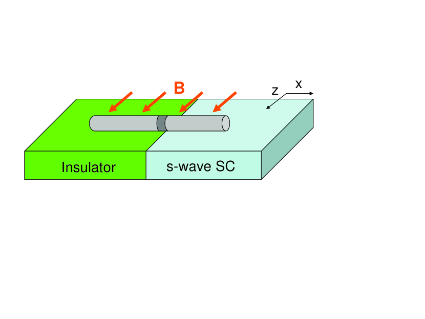
In this paper, we propose to detect Majorana fermions in a more common and robust charge transport type of experiments Wimmer in the semiconductor/superconductor heterostructure. The proposed experimental setup is illustrated in Fig. 1, where one section of the semiconductor nanowire is in proximity contact with an s-wave superconductor, while the other is in contact with an insulator. The electrical conductance is measured between the two ends of the semiconductor nanowire. At the interface between these two sections of the nanowire, the transport of electrons is described by the Andreev reflection (AR)Andreev . It is well known that when a normal metal is in contact with a superconductor, AR process dominates the charge transport if the energy of the incident particle lies inside the gap of the superconductor. AR is also a useful tool to measure spin polarization of ferromagnet Jong ; Upadhyay ; Soulen and to probe unconventional superconductor Deutscher ; Sengupta ; Tanaka2 . Recently, AR has been studied in topological insulators to explore their exotic properties Law ; Linder ; Tanaka ; Nilsson .
Because Majorana fermions occupy the zero energy state in the superconductor, their signature is generally expected to be a peak of the electrical conductance at the zero external voltage. However, in the regular AR between a normal metal (or semiconductor) and a regular s-wave superconductor, the electrical conductance is already the constant when the energy of the incident electron is in the superconductor gap regionBlonder . Therefore the signature of Majorana fermions may be hidden in the large regular AR signals and cannot be observed in experiments. In previous literature, the constant electrical conductance in the gap region can be removed by adding an insulating barrier between the metal and the superconductorBlonder . Here we adopt the same approach and use an insulating (or potential) barrier to prevent the regular AR between the sections of the semiconductor nanowire with and without the contact with the s-wave superconductor.
In this paper, we find that when the section of the nanowire in contact with the superconductor is in the topological state, there is a zero-bias peak in the electrical conductance. This zero energy peak originates from the Majorana fermions existing at the interface between the superconducting and normal states, which induces a resonant AR of electrons although the normal AR is strongly suppressed by the high potential barrier at the interface. The width of the zero energy conductance peak depends on the barrier height as well as the spin-orbit coupling strength. When the section of the nanowire in contact with the superconductor is in the non-topological state without Majorana fermions, there is no resonant AR at the zero energy and the zero-bias conductance peak disappears. In this case, the electrical conductance depends strongly on the number of conduction bands intercepted by the chemical potential. When only one conduction band is occupied by electrons, the electrical conductance at the zero bias is suppressed to zero Fisher ; Wimmer , but increases with the increasing bias voltage. When both conduction bands are occupied, the suppression of the zero bias conductance in the single band case vanishes and the electrical conductance is similar as that for a junction between a normal metal and a regular s-wave superconductor. Finally, we find that the zero-bias peak disappears in a two-dimensional semiconductor thin film in contact with an s-wave superconductor where the zero energy Majorana modes coexist with other edge modes with non-zero momentum and energy, which contribute to the conductance signals at the non-zero energy.
The paper is organized as follows: Section II describes the proposed experimental setup and the Hamiltonian. Section III discusses the electrical conductance of the nanowire calculated using the Blonder-Tinkham-Klapwijk (BTK) theoryBlonder . We study the dependence of the electrical conductance on the spin-orbit coupling strength, the Zeeman field, and the barrier height. We extend our model and method to a two-dimensional semiconductor thin film in section IV. Section V consists of the discussion and conclusion.
II Proposed experimental scheme and the Hamiltonian
The proposed experimental scheme is shown in Fig. 1. The semiconductor nanowire lying along the direction is deposited on the top of an insulator and an -wave superconductor heterostructure. Due to the proximity effect, the -wave Cooper pairs can tunnel into the right section of the nanowire (), yielding a non-zero superconducting pairing order parameter . In the left section of the nanowire (), . A magnetic field is applied along the direction, yielding a Zeeman field , where is the Landé factor, is the Bohr magnet. An insulating barrier (or potential) is applied at the interface between these two sections of the nanowire. Such a potential barrier may be realized by growing a thin junction with a different type of material around during the growth of the nanowireLiber ; Pitanti , or by applying a gate voltage on the nanowire at .
The dynamics of electrons in the semiconductor nanowire can be described by the Bogoliubov-de-Gennes (BdG) equation. In the Nambu spinor space, the BdG equation can be written as , where the BdG Hamiltonian
| (1) |
with the quasiparticle wavefunction , where and are the particle and hole wavefunctions respectively. The single particle Hamiltonian
| (2) |
where is the effective mass of the electron, is the Rashba spin-orbit coupling interaction, is the perpendicular Zeeman field, is the chemical potential in the semiconductor which is controlled by the density of doped electrons. For simplicity, we use to model the barrier potential at . The superconducting order parameter , where the step function when and when .
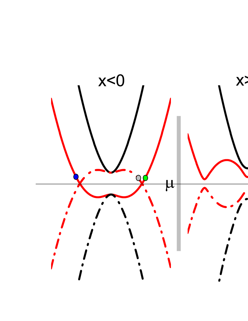
The energy spectrum for the left and right sections of the heterostructure is plotted in Fig. 2. In the left section () with , it is just the single particle spectrum determined by , which has two bands with the energy dispersion
| (3) |
The energy gap at is . Henceforth we set . When the chemical potential lies in the gap, electrons only occupy the lower spin-orbit band at a low temperature. To compare with the superconducting spectrum in the right section of the nanowire (), the spectrum for the hole Hamiltonian is also plotted.
With the non-zero superconducting order parameter in the right section, the bulk quasiparticle excitation spectrum becomes
| (4) |
where . Around the Fermi surface, a bulk gap is always opened between the middle two bands due to the superconducting coupling between the particle and hole branches. However, in contrast to a regular s-wave superconductor where the minimum energy gap appears around the Fermi surface, the minimum energy gap in the spin-orbit coupled system may appear at . In fact, the energy gap at disappears when
| (5) |
although the superconducting order parameter is nonzero. When , the system is in a regular s-wave non-topological state without Majorana fermions. While when , the system is in a topological quantum state with Majorana fermions at . Across , the change of the Zeeman field defines a topological phase transition from a non-topological superconductor to a topological superconductor Sau1 . For the simplicity of the calculation, in the following we consider three different cases: (i) , and (topological state); (ii) , and (non-topological state with one conduction band occupied by electrons); (iii) (non-topological state with two conduction bands occupied by electrons). We have confirmed that the results for other parameters are similar.
III Electrical conductance of the nanowire
The electrical conductance along the nanowire can be calculated based on the BTK theory Blonder ; Mizuno ; Linder2 , where the wavefunctions at both sides of the potential barrier are constructed and matched at . We first consider cases (i) and (ii). The wavefunction in the left section of the nanowire can be obtained analytically as
where the wavevectors are defined as
, . and are AR coefficients for the lower and higher bands
respectively. and are the corresponding normal reflection
coefficients. and are the normalization
constants of the wavefunctions. Since the chemical potential lies between
two spin-orbit bands in cases (i) and (ii), there is no plane wave solution
for the higher band, and decaying wavefunctions have been used in Eq. (6).
Because of the superconducting proximity effect, analytical expressions for
the wavefunction in the right section of the nanowire are not available.
Instead, we numerically solve the eigenvalue equations and find the
corresponding transmitted wavefunction for different incident
particle energy .
The wavefunctions and its derivative should be matched at the interface between two sections, where is the velocity matrix determined by the Hamiltonian (1). The reflection and transmission coefficients are calculated by solving the resulted linear equations for the unknown coefficients. The electrical conductance along the nanowire is
| (7) |
with () is the Andreev (normal) reflection coefficient in the lower band of , is the electrical conductance of the nanowire without the superconductor and the magnetic field. Because the wavefunctions in the higher band are evanescent waves when the chemical potential lies inside the gap between two spin-orbit bands, the Andreev and normal reflection coefficients in the higher band do not contribute to the electrical conductance and thus have been neglected. However, the higher band wavefunctions on both sides of must be included in the calculation for a self-consistent solution, where the number of unknown coefficients should match with the number of linear equations determined by the boundary conditions at . In addition, we are only interested in AR which dominates the electron transportation in the superconducting gap region on the side, therefore we restrict the incident electron energy less than the minimum quasiparticle energy gap in our calculation.
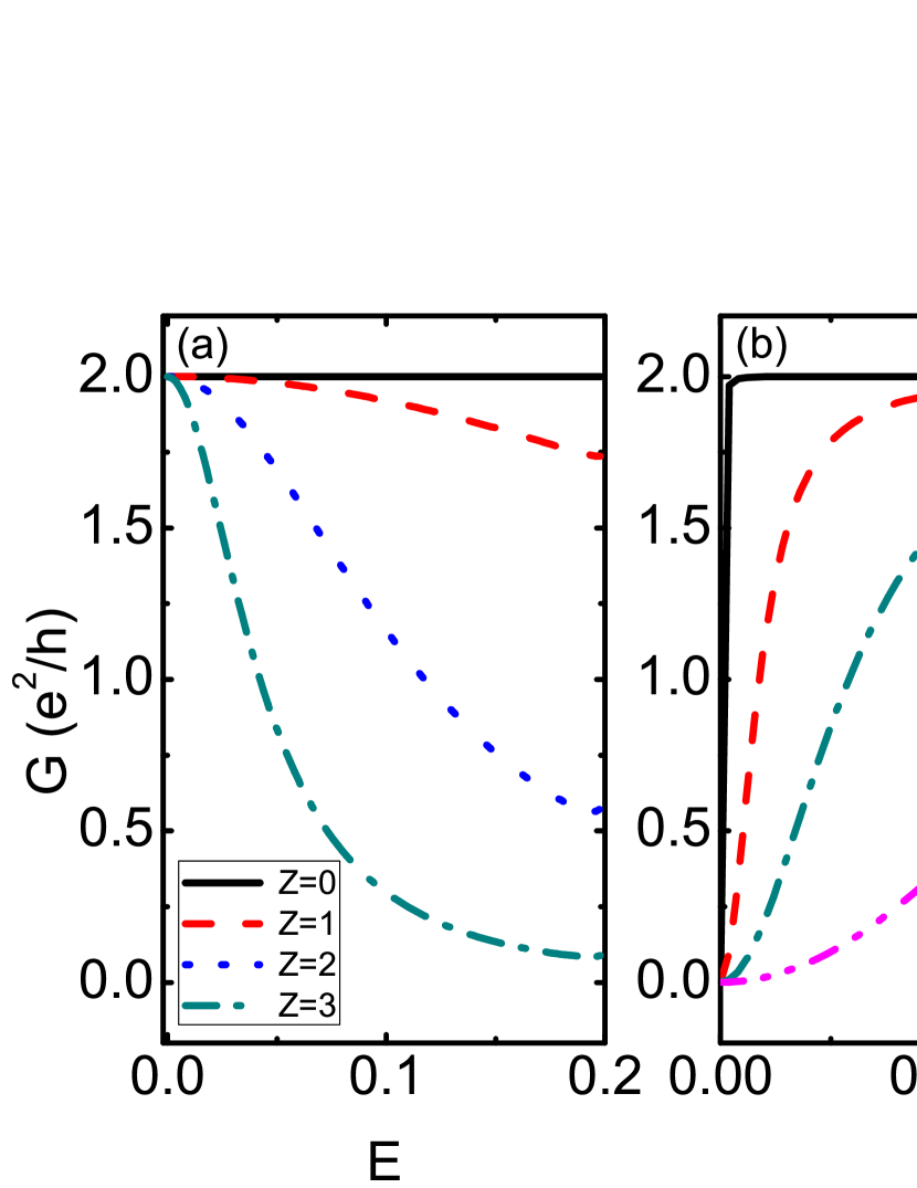
The dependence of the electrical conductance as a function of the incident electron energy is plotted in Fig. 3 for different parameters. In the calculation for Fig. 3b, we restrict to the energy region rather than because the minimum quasiparticle excitation gap is (occurs at when is small), instead of at the Fermi surface. In Fig. 3a, the Zeeman field for the topological state that supports Majorana zero energy modes at Sau1 ; Roman1 , while in Fig. 3b for the non-topological state without Majorana fermions. All parameters are re-scaled to dimensionless forms. The energy unit for , , and is chosen as , and the unit for is , where is a suitable chosen wavevector to match with the experimental values of . For InAs nanowire, the typical parameters are , eV Å, K, K. As mentioned before, has been used in the calculation.
In Fig. 3, different lines correspond to different values of the barrier height . For a regular non-topological superconductor (Fig. 3b) without the insulating barrier (), the charge transport in the superconducting gap region is dominated by the regular AR. If there is no spin-orbit coupling, the degeneracy between spin up and down electrons is lifted by the Zeeman field, and there is only one single channel for the AR when the chemical potential lies in the Zeeman gap. In this case, the AR is strongly suppressed and the electrical conductance is very small Fisher . The existence of spin-orbit coupling greatly enhances the AR at the finite , but the electrical conductance is still zero at when only a single spin-orbit conduction band is occupied Wimmer , as clearly seen from Fig. 3b. For a large spin-orbit coupling, the regular AR dominates at the finite , that is, and . Therefore is a constant, as observed. With the increasing barrier height , the AR coefficient decreases and normal reflection coefficient increases. For a very large , the amplitude of the AR should be zero (i.e., , and ) because the incident electrons are reflected completely by the high barrier, leading to a vanish . However, the existence of the Majorana zero energy mode at in the topological state (Fig. 3a) leads to a resonant AR Law , which gives a resonant peak at even for a large barrier height . The resonant tunneling (thus the conductance) is the largest at the zero energy, but decreases quickly at the finite energy for a large barrier potential, as observed in Fig. 3a.
In Fig. 4, we plot the conductance peak width (defined by the energy with ) with respect to the barrier height (Fig. 4a) and spin-orbit coupling strength (Fig. 4b) for the topological state (Fig. 3a) with Majorana fermions. We see that as the barrier height increases, the conductance peak is narrower, as expected. When the spin-orbit coupling increases, the conductance peak width is wider and the signature of the Majorana fermions is more clear. In a practical experiment, we should adopt a large barrier height to eliminate the regular AR, and a large spin-orbit coupling to enhance the resonant AR induced by the Majorana fermions.

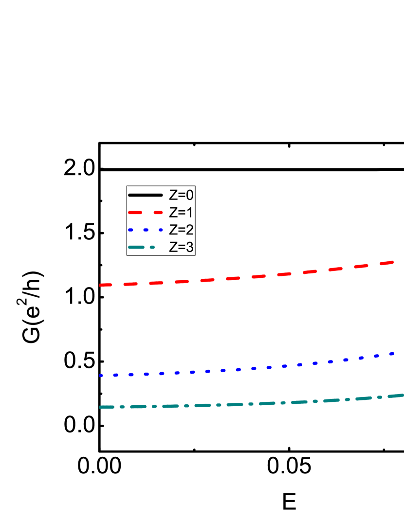
We now consider the case (iii) where the chemical potential intercepts two conduction bands and there are no topological superconducting states. In this case, in the wavefunction (6) becomes imaginary and there exist plane wave solutions for the high spin-orbit coupled band. Following similar procedure, we calculate the electrical conductance and plot it in Fig. 5. In this case, the electrical conductance is for even at because of the two AR channels, which is different from that in Fig. 3b for a single AR channel. With the increasing barrier height , the electrical conductance reduces smoothly for all in the gap region, similar as that for a junction between a normal metal and a regular s-wave superconductor.
IV Electrical conductance in a semiconductor thin film
In the above section, we have shown the signature of Majorana fermions in semiconductor nanowires in a charge transport type of experiment. Note that Majorana fermions are also proposed to exist in a two-dimensional semiconductor thin film in proximity contact with an s-wave superconductor and a magnetic insulator Sau1 ; Mao1 . Therefore it is natural and interesting to study whether similar transport signature can be observed in such a 2D semiconductor heterostructure, where the single particle Hamiltonian in Eq. (1) should be replaced with
| (8) |
The energy spectrum of in the momentum space is the same as that for the nanowire (Fig. 2) with the substitution . In the 2D semiconductor thin film, the perpendicular magnetic field in the nanowire (Fig. 1) is replaced with a magnetic insulator in proximity contact with the thin film to avoid orbital effects (such as unwanted vortices) induced by the magnetic field. On the side, the thin film is still in contact with an s-wave superconductor. In this system, the translational symmetry is broken along the direction but conserved along the direction, therefore is a good quantum number.
The electrical conductance of the semiconductor thin film heterostructure is calculated following the same procedure as that for the semiconductor nanowire. The system can support Majorana zero energy states at the interface . The results for the normal incidence, i.e., , are similar as the nanowire: depending on the magnitude of the Zeeman field, Majorana zero energy mode exists or disappears, which are characterized by the emergence or disappearance of the conductance peak at the zero incident energy. Therefore here we only show the results for .
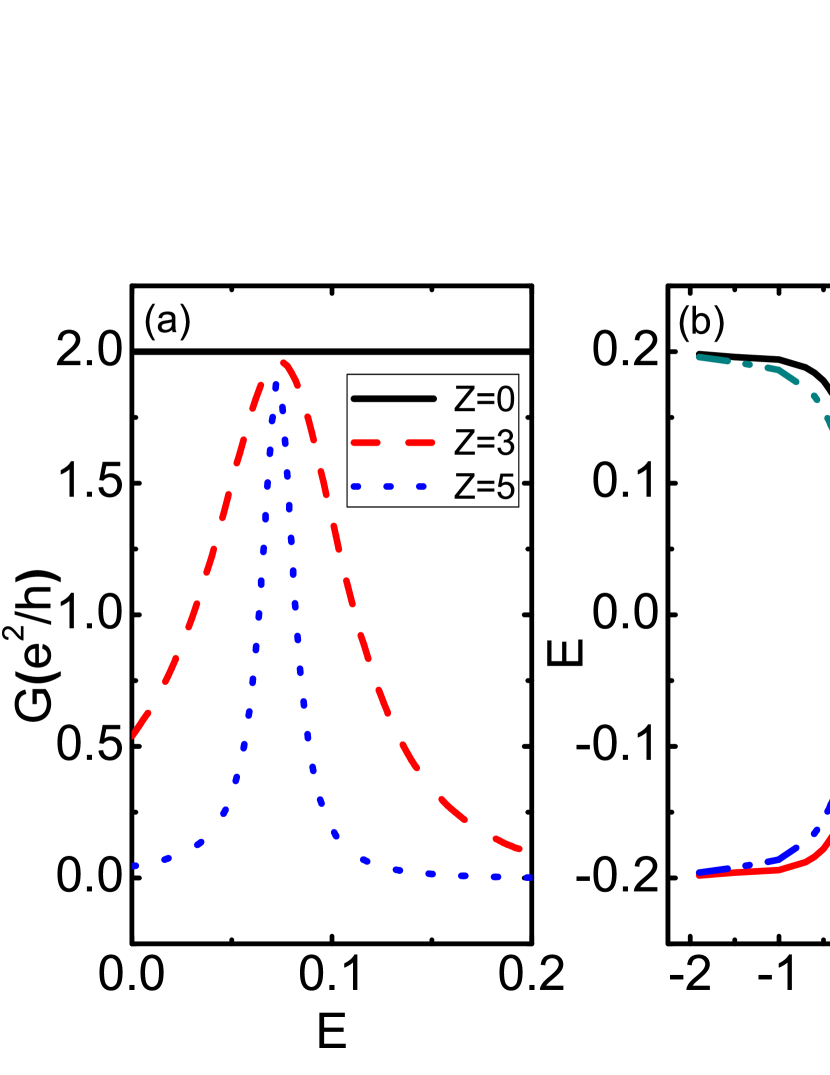
For certain value of , we find that there is a conductance peak existing inside the bulk gap (see Fig. 6a) in the parameter region . While the peaks vanishes when . However, the peak occurs at certain finite value of inside the gap, which is different from the peak at for . The center the conductance peak moves away from with the increasing . This phenomena can be understood from the edge states Hasan at the interface . In the 2D heterostructure at , the edge state at has an energy dispersion relation inside the bulk gap between the particle and hole branches of the BdG Hamiltonian (1). The edge state at can induce a resonant AR for electrons with energy around , leading to a conductance peak. In Fig. 6b, we plot the energy dispersion for the edge state, which has the following properties: (1) the chirality of the dispersion (i.e., increase or decrease with increasing ) is determined by the sign of the perpendicular Zeeman field; (2) the slope of the energy dispersion (i.e., the velocity of electrons in the edge state) is determined by the magnitude of the Zeeman field: the smaller the magnetic field, the steeper the dispersion. We note that these two properties are the same as that of the Andreev-bound state dispersion in the junction composed of a magnetic insulator and an s-wave superconductor on the surface of a topological insulator Linder2 .
In a practical experiment, the incident electron beam may contain different due to the scattering to different angles from the interface, therefore the conductance should be the summation over the signals from different . Since the edge states at other also give peaks at non-zero through resonant AR (although the peak height does drop slightly with the increasing ), it is hard to extract signals for the Majorana zero energy states. Therefore the semiconductor nanowire would be a better system for the observation of Majorana fermions than the semiconductor thin film in the charge transport type of experiments.
V Conclusion
In summary, we study the transport properties along a semiconductor nanowire which is partially in proximity contact with an s-wave superconductor and subject to a perpendicular magnetic field. We find that Majorana fermions existing in a certain parameter region and at the interface between the superconducting and normal parts of the nanowire can induce resonant AR, which yields a zero energy peak in the transport electrical conductance. We characterize the properties of the peak for different experimental parameters. We show that such zero energy conductance peak disappears in a 2D semiconductor thin film with the same setup because of the existence of other edge states in 2D. We believe our proposed transport experiment provides a simple and experimental feasible way for the experimental detection of Majorana fermions. Finally, although the calculation is done for electron-doped semiconductor nanowires, the Majorana fermions induced zero energy conductance peaks should also be observable in hole-doped semiconductor nanowires Mao3 , where Majorana fermions exist with a higher carrier density and a lower magnetic field, and thus may be more experimentally accessible.
Acknowledgement–We thank M. Wimmer for helpful discussion. This work is supported by DARPA-MTO (FA9550-10-1-0497), DARPA-YFA (N66001-10-1-4025), and NSF-PHY (1104546).
References
- (1) E. Majorana, Nuovo Cimento 5, 171 (1937).
- (2) G. Moore, and N. Read, Nucl. Phys. B 360, 362 (1991).
- (3) C. Nayak, and F.Wilczek, Nucl. Phys. B 479, 529 (1996).
- (4) N. Read, and D. Green, Phys. Rev. B 61, 10267 (2000).
- (5) S. Das Sarma, M. Freedman, and C. Nayak, Phys. Rev. Lett. 94, 166802 (2005).
- (6) D. A. Ivanov, Phys. Rev. Lett. 86, 268 (2001).
- (7) S. Das Sarma, C. Nayak, and S. Tewari, Phys. Rev. B 73, 220502 (2006).
- (8) M. Stone and S. B. Chung, Phys. Rev. B 73, 014505 (2006).
- (9) S. S. Botelho and C. A. R. Sa de Melo, J. Low Temp. Phys. 140, 409 (2005).
- (10) V. Gurarie, L. Radzihovsky, and A. V. Andreev, Phys. Rev. Lett. 94, 230403 (2005).
- (11) C.-H. Cheng and S.-K. Yip, Phys. Rev. Lett. 95, 070404 (2005).
- (12) S. Tewari, S. Das Sarma, C. Nayak, C. Zhang, and P. Zoller, Phys. Rev. Lett. 98, 010506 (2007).
- (13) L. Fu and C. L. Kane, Phys. Rev. Lett. 100, 096407 (2008).
- (14) L. Fu and C. L. Kane, Phys. Rev. Lett. 102, 216403 (2009).
- (15) A. R. Akhmerov, J. Nilsson, and C. W. J. Beenakker, Phys. Rev. Lett. 102, 216404 (2009).
- (16) Y. Tanaka, T. Yokoyama, and N. Nagaosa, Phys. Rev. Lett. 103, 107002 (2009).
- (17) J. D Sau, R. M. Lutchyn, S. Tewari, and S. Das Sarma, Phys. Rev. Lett. 104, 040502 (2010).
- (18) J. D. Sau, S. Tewari, R. M. Lutchyn, T. D. Stanescu, and S. Das Sarma, Phys. Rev. B 82, 214509 (2010)
- (19) J. Alicea, Phys. Rev. B 81, 125318 (2010).
- (20) R. M. Lutchyn, J. D. Sau, and S. Das Sarma, Phys. Rev. Lett. 105, 077001 (2010).
- (21) Y. Oreg, G. Refael, and F. von Oppen, Phys. Rev. Lett. 105, 177002 (2010).
- (22) R. M. Lutchyn, T. D. Stanescu, and S. Das Sarma, Phys. Rev. Lett. 106, 127001 (2011).
- (23) L. Mao, and C. Zhang, Phys. Rev. B 82, 174506 (2010).
- (24) L. Mao, J. Shi, Q. Niu, and C. Zhang, Phys. Rev. Lett. 106, 157003 (2011).
- (25) L. Mao, M. Gong, E. Dumitrescu, S. Tewari, and C. Zhang, arXiv: 1105.3483.
- (26) A. Kitaev, Ann. Phys. (N.Y.) 303, 2 (2003).
- (27) C. Nayak, S. H. Simon, A. Stern, M. Freedman, and S. Das Sarma, Rev. Mod. Phys. 80, 1083 (2008).
- (28) C. Zhang, S. Tewari, R. M. Lutchyn, and S. Das Sarma, Phys. Rev. Lett. 101, 160401 (2008).
- (29) M. Sato, Y. Takahashi, and S. Fujimoto, Phys. Rev. Lett. 103, 020401 (2009).
- (30) K. Flensberg, Phys. Rev. B Phys. Rev. B 82, 180516(R) (2010).
- (31) A. Y. Kitaev, Phys. Usp. 44, 131 (2001).
- (32) L. Fu and C. L. Kane, Phys. Rev. B 79, 161408(R) (2009).
- (33) H. J. Kwon, K. Sengupta, and V. M. Yakovenko, Eur. Phys. J. B 37, 349 (2003).
- (34) M. Wimmer, A. R. Akhmerov, J. P. Dahlhaus and C. W. J. Beenakker, New J. Phys. 13, 053016 (2011).
- (35) A. F. Andreev, Sov. Phys. JETP 19, 1228 (1964).
- (36) M. J. M. de Jong and C. W. J. Beenakker, Phys. Rev. Lett. 74, 1657 (1995).
- (37) S. K. Upadhyay, A. Palanisami, R. N. Louie, and R. A. Buhrman, Phys. Rev. Lett. 81, 3247 (1998).
- (38) R. J. Soulen Jr., J. M. Byers, M. S. Osofsky, B. Nadgorny, T. Ambrose, S. F. Cheng, P. R. Broussard, C. T. Tanaka, J. Nowak, J. S. Moodera, A. Barry and J. M. D. Coey, Science, 282, 85 (1998).
- (39) G. Deutscher, Rev. Mod. Phys. 77, 109 (2005).
- (40) K. Sengupta and Victor M. Yakovenko, Phys. Rev. Lett. 101, 187003 (2008).
- (41) Y. Tanaka, T. Yokoyama, A. V. Balatsky, and N. Nagaosa, Phys. Rev. B 79, 060505(R) (2009).
- (42) K. T. Law, P. A. Lee, and T. K. Ng, Phys. Rev. Lett. 103, 237001 (2009).
- (43) J. Linder, Y. Tanaka, T. Yokoyama, A. Sudbø and N. Nagaosa, Phys. Rev. Lett. 104, 067001 (2010).
- (44) Y. Tanaka, T. Yokoyama, and N. Nagaosa, Phys. Rev. Lett. 103, 107002 (2009).
- (45) J. Nilsson, A. R. Akhmerov, and C. W. J. Beenakker, Phys. Rev. Lett. 101, 120403 (2008).
- (46) G. E. Blonder, M. Tinkham, and T. M. Klapwijk, Phys. Rev. B25, 4515 (1982).
- (47) M. P. A. Fisher, Phys. Rev. B 49, 14550 (1994).
- (48) M. S. Gudiksen, L. J. Lauhon, J. Wang, D. C. Smith, and C. M. Lieber, Nature 415, 617 (2002).
- (49) A. Pitanti, D. Ercolani, L. Sorba, S. Roddaro, F. Beltram, L. Nasi, G. Salviati, and A. Tredicucci, Phys. Rev. X 1, 011006 (2011).
- (50) Y. Mizuno, T. Yokoyama, and Y. Tanaka, Phys. Rev. B80, 195307 (2009).
- (51) J. Linder, Y. Tanaka, T. Yokoyama, A. Sudbø and N. Nagaosa, Phys. Rev. B 81, 184525 (2010).
- (52) M. Z. Hasan and C. L. Kane, Rev. Mod. Phys. 82, 3045 (2010).