Phonon-drag induced suppression of the Andreev hole current in superconducting niobium contacts
Abstract
We have investigated how the Andreev-reflection hole current at ballistic point contacts responds to a large bias voltage. Its strong suppression could be explained by the drag excerted by the non-equilibrium phonon wind generated by high-energy electrons flowing through the contact. The hole - phonon interaction leads to scattering lengths of the low-energetic holes down to 100 nm, thereby destroying the coherent retracing of the electron path by the Andreev-reflected holes.
I Introduction
The Andreev reflection hole current at ballistic normal - superconducting point contacts can be reduced by many mechanisms: normal reflection, finite Cooper pair life time, and spin polarization produce characteristic anomalies and represent the material and device properties that we are usually interested in Tuuli2011 . Others are associated with locally exceeding the superconducting critical temperature, field, or the condensation energy Gloos2009 . They result in sharp structures or side peaks of the spectra which can be easily reckognized. However, they are difficult to handle because of their strong dependence on the geometric shape of the contact. Another mechanism causes broad side peaks at finite bias voltage that have neither well-defined beginning nor end. They add considerable uncertainty in the analysis of the spectra. We suggest here that those broad maxima origin from the interaction of the Andreev reflection hole current with the wind of non-equilibrium phonons generated at large bias voltages.
In a previous study on point contacts between ultra-high purity superconducting tantalum (Ta) and normal conducting silver (Ag), Hahn et al. Hahn2002 have found anomalies in the spectra that they interpreted in terms of a huge normal bubble - or ’hot spot’ - inside the superconductor. They assumed that high-energy electrons are resonantly trapped between the normal - superconductor interface of the hot spot itself and the contact. Such a normal bubble would extend up to several times the superconducting coherence length of Ta. This length scale was supported by observing interference phenomena in a magnetic field Hahn1995 .
While Hahn et al. Hahn2002 ; Hahn1995 were mainly interested in the resonances that appeared in the spectra to explain their observation, we have used a different approach based on the AR hole current derived from the difference of the measured normal and superconducting current-voltage characteristics of superconducting niobium (Nb) in contact with a normal metal.
II Experimental
Our point contacts were fabricated using the shear method where the two sample wires (typically mm diameter) were brought into contact in the form of a cross. The differential resistance and the characteristics were recorded in standard four-wire mode with low-frequency current modulation.
The thermal coupling between the contact, through the sample wires and their anchorage, to the cooling stage at temperature was measured by injecting a large power into the contact and using the critical temperature K of Nb as marker for the contact turning normal. This heating of the contact is described by with the Lorenz number and an equivalent thermal resistance m. An other upper bound for the local temperature distribution in the point contact is given by Kohlrausch’s formula Kohlrausch1900 . This is valid in the thermal limit, while in the diffusive and the ballistic regime the temperature differences are much smaller.
To measure the Andreev reflection excess current directly, we recorded the contact characteristics both at low temperature (1 K) in the superconducting and at high temperature (10 K) in the normal state of Nb. This required thermal cycling until the contact stabilized and which worked well for normal-state contact resistances up to or contact diameters down to around nm.
III Results
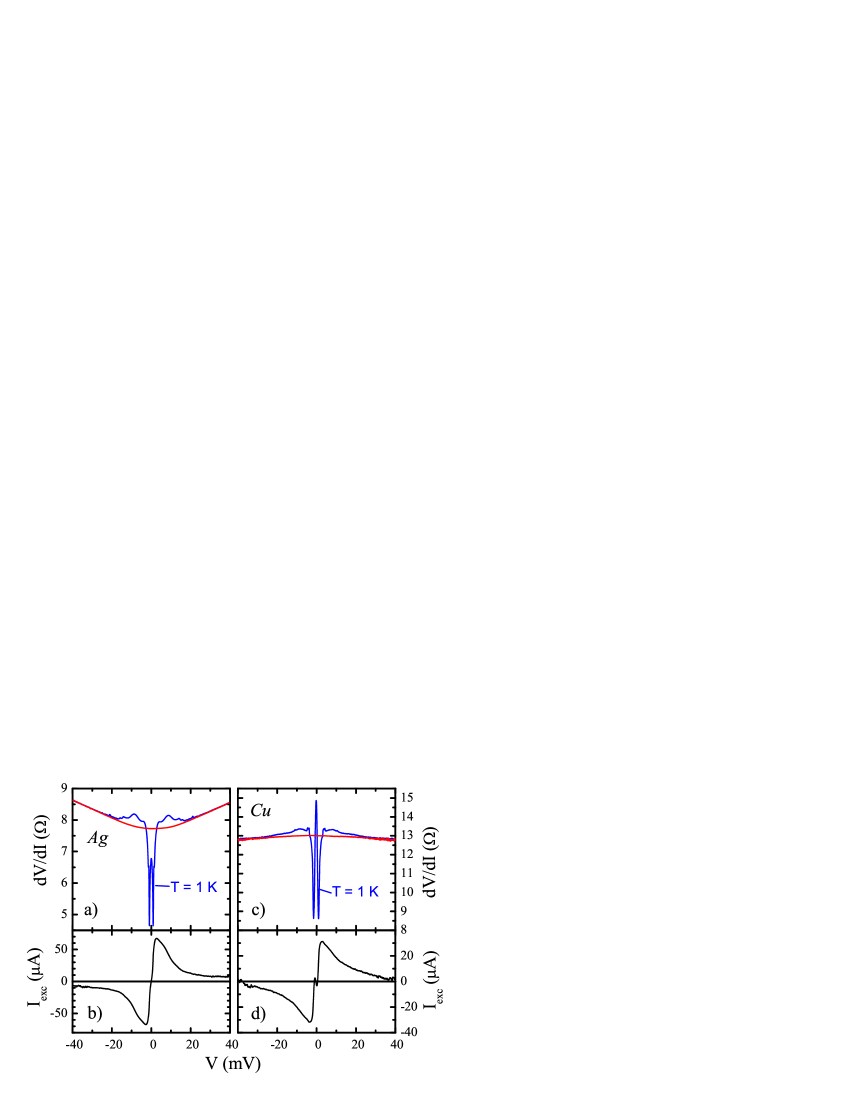
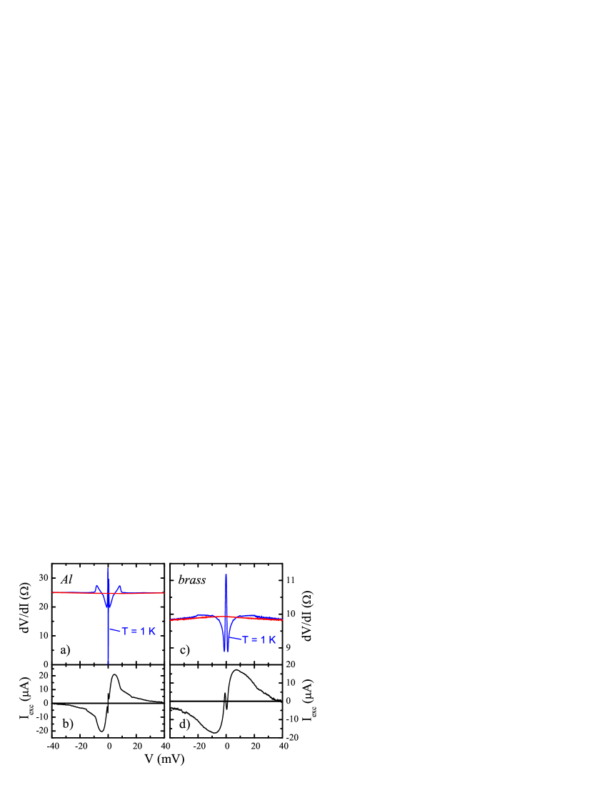
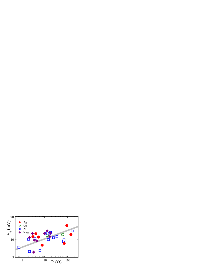
Figures 1 and 2 show typical spectra of Nb in contact with Ag, copper (Cu), aluminum (Al), and brass at K and at K as reference. They look qualitatively similar to those observed by Hahn et al. Hahn2002 for Ta - Ag contacts. The spectra have the typical Andreev-reflection double-minimum anomaly (except the contacts with Al) and also broad side peaks with a superposed fine structure. At large voltages the spectra in the superconducting and the normal state coincide. The magnitude of the excess current drops continuously with increasing bias voltage which can roughly be described by . Some of the contacts had a small residual excess current at large voltages, possibly due to a reversible change of the contact upon thermal cycling. We have observed similar behaviour for all Nb - normal metal contacts. Figure 3 summarizes the decay constant of the excess current as function of normal-state contact resistance. It increases only slightly with and it apparently does not depend on the normal metal.
IV Discussion
At large bias voltage heating might become a problem. From the measured thermal coupling of the samples we estimate maximum temperatures that are still far below of Nb. The weak dependence of on the contact size also excludes heating effects, because heating at a contact would be 100 times stronger than at a contact, assuming the same bias voltage. This would contradict the experimental data in Figure 3.
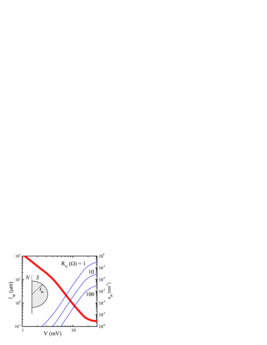
To avoid the ad hoc assumptions of specific boundary conditions used by Hahn et al. Hahn2002 , we want to find a more conventional interpretation of the experiments. A rather straightforward mechanism to reduce the excess current without heating is electron scattering at the non-equilibrium phonons generated by the bias voltage Jansen1980 . Figure 4 shows the calculated electron - phonon scattering length at low temperatures using derived from the measured electron-phonon interaction function Khotkevich1995 and a Fermi velocity Ashcroft1976 m/s of Nb. At large voltages is comparable to the superconducting coherence length nm of Nb. We estimate the density of excess phonons as follows: Phonons are generated at the point-like contact at a rate of , that is one phonon per injected electron. The phonon density is constant inside a half-sphere of radius around the contact. They escape from this volume with sound velocity m/s of niobium at a rate . Thus in the stationary state . These excess phonons scatter the low-energy holes with a mean-free path comparable to that of the high-energy electrons and destroy the coherence of Andreev reflection. Such a scattering event deflects the hole from the path of the incident electron and thereby reduces its chances to fly back through the contact, thereby reducing the Andreev-reflection excess current.
Since ballistic electrons have a preferred forward direction, a cone would be more appropriate than a half-sphere. This would lead to a larger phonon density by reducing the volume and decreasing the area from which phonons can escape. In addition, each electron could create more than just a single phonon. Also the target area for the holes becomes smaller with increasing contact resistance which could explain the very weak dependence.
Our model also explains why some of the contacts have pronounced maxima and side peaks while others have very small anomalies. Large maxima of the type discussed here require the presence of an excess current which can be suppressed, that is such a contact has little normal reflection and a small polarization as well as a long Cooper pair lifetime. To extract those parameters from the measured spectra one should use the part around zero bias with a reasonable estimate of the normal contact resistance, and ignore - as much as possible - the side peaks.
V Conclusions
The suggested scenario offers no way to overcome the side-peak problem because generating non-equilibrium phonons is an intrinsic property of the material and the contacts, and inherent to measuring the spectra. This makes a precise measurement of the energy gap of superconductors with large and large difficult. Side peaks can be avoided only when the superconductor has a small gap and the voltage range can be kept sufficiently small.
VI acknowledgements
We thank the Jenny and Antti Wihuri Foundation and the Magnus Ehrnroot Foundation for financial support.
References
- (1) Tuuli E and Gloos K 2011 Fiz. Nizk. Temp. 37 609
- (2) Gloos K and Sjölund J 2009 J. Phys.: Conf. Ser. 150 052061
- (3) Hahn A, Hofmann S, Hümpfner K and Schatz M 2002 Phys. Rev. B 65 224503
- (4) Hahn A and Hümpfner K 1995 Phys. Rev. B 51 3660
- (5) Kohlrausch F 1900 Ann. Phys., Lpz. 1 132
- (6) Jansen A G M, van Gelder A P and Wyder P 1980 J. Phys. C 13 6073
- (7) Khotkevich A V and Yanson I K 1995 Atlas of point contact spectra of electron-phonon interactions in metals (Kluwer Academic Publishers)
- (8) Ashcroft N W and Mermin N D 1976 Solid State Physics (Thomson Learning)