Direct measurement of quantum phases in graphene via photoemission spectroscopy
Abstract
Quantum phases provide us with important information for understanding the fundamental properties of a system. However, the observation of quantum phases, such as Berry’s phase and the sign of the matrix element of the Hamiltonian between two non-equivalent localized orbitals in a tight-binding formalism, has been challenged by the presence of other factors, e. g. , dynamic phases and spin/valley degeneracy, and the absence of methodology. Here, we report a new way to directly access these quantum phases, through polarization-dependent angle-resolved photoemission spectroscopy (ARPES), using graphene as a prototypical two-dimensional material. We show that the momentum- and polarization-dependent spectral intensity provides direct measurements of (i) the phase of the band wavefunction and (ii) the sign of matrix elements for non-equivalent orbitals. Upon rotating light polarization by , we found that graphene with a Berry’s phase of ( 1 for single- and 2 for double-layer graphene for Bloch wavefunction in the commonly used form) exhibits the rotation of ARPES intensity by , and that ARPES signals reveal the signs of the matrix elements in both single- and double-layer graphene. The method provides a new technique to directly extract fundamental quantum electronic information on a variety of materials.
pacs:
79.60.Jv, 03.65.Vf, 31.15.aq, 81.05.ue, 73.22.PrI Introduction
Quantum phases are the most beautiful example of quantum physics and essential to understand physics in any material. For example, Berry’s phase, the accumulated phase in the eigenfunction acquired by evolving the quantum system adiabatically around a closed loop in the parameter space of the Hamiltonian Bohm , has been shown to be responsible for the Aharonov-Bohm effect Aha , the half-integer quantum Hall effect Zhang ; Novoselov ; McCann , etc. Another important example is the sign of the hopping matrix element (or hopping integral) of the Hamiltonian between two non-equivalent localized orbitals and in a tight-binding formalism. This phase, a fundamental quantity in determining the electronic structure of a system, is dictated by the characteristics of the atomistic interaction, e. g. , whether it is attractive or repulsive. Both of these are important to directly extract fundamental quantum electronic information on a variety of materials Taguchi ; Murakami ; Hsieh .
In graphene, the Berry’s phase is theoretically extracted from the spinor eigenstate, which are for single- and for double-layer graphene McCann . From recent studies, the Berry’s phase in the commonly used form of the spinor states is, in fact, related to the pseudospin winding number of a particle as it travels in a loop in -space which encloses the Dirac point Parkcond . These values have been measured through magneto-transport experiments Zhang ; Novoselov that are typically neither capable of measuring Berry’s phase of a specific electron bandstructure nor free from spin/valley degeneracy of the electron bandstructure of a system under study. Additionally, this method requires a strong magnetic field, which breaks time-reversal symmetry in graphene. Meanwhile, the signs of hopping integrals between non-equivalent orbitals for graphene (graphite) have only been determined by ab initio calculations Gruneis , e. g. , using maximally localized Wannier functions Marzari . Since the sign of hopping integral depends on the characteristics of the localized orbitals and the interaction between them, it is crucial in determining the electron bandstructure within a tight-binding formalism. However, the absence of methodology has led to use the signs following the well-known Slonczewski-Weiss-McClure model SWMc1 ; SWMc2 without experimental verification for the past few decades. Additionally, the sign of hopping integral between non-equivalent orbitals has never been determined experimentally for any material.
Given the high momentum-resolving power of angle-resolved photoemission spectroscopy (ARPES), ARPES is an ideal candidate to solve the above issues on the determination of quantum phases. For example, the phase difference between the matrix elements describing two different optical transitions at the (110) surface of platinum was extracted from a combined study of a spin-resolved ARPES experiment and a theoretical model YuPt . Also, ARPES has been employed to study the characteristics of the spinor eigenstates in graphite Himpsel and graphene Eli , which revealed an interference effect between photo-excited electrons Himpsel ; Eli . However, these theoretical studies, within a tight-binding formalism, have incorrectly treated the interaction Hamiltonian, which is the key part in the photoemission process as it describes the interaction between photons and electrons. Moreover, it has not been clear how Berry’s phase enters in ARPES intensity and the sign of hopping integral has only been speculated without any comparison with experiments Eli , which naturally leads to incorrect values.
Here we report that ARPES can indeed provide information on these quantum phases, e. g. , the Berry’s phase and the sign of hopping integral between non-equivalent orbitals. The phase factor in the spinor eigenstate of graphene McCann gives rise to strong intensity variation around a constant energy contour. Upon rotating light polarization by , we found that graphene with a Berry’s phase of ( 1 for single- and 2 for double-layer graphene) exhibits the rotation of ARPES intensity maxima by , which gives important advantages compared to the conventional magneto-transport method Zhang ; Novoselov . Additionally, we found that full polarization-dependence of ARPES signal reveals the sign of hopping integrals in both single- and double-layer graphene (graphite can also be understood), e. g. , and , which is the first experimental determination of the sign of hopping integral between non-equivalent orbitals for any material by any method.
II Sample preparation
Single- and double-layer graphene samples were grown epitaxially on -doped 6-SiC(0001) surfaces by electron-beam heating, as detailed elsewhere Rollings . An SiC sample was mounted in a prep-chamber with a base pressure of 510-10 Torr to remove a thick oxide layer from the sample by heating at 600 ∘C for a few hours. The clean sample was then transferred to a custom-designed chamber equipped with low-energy-electron microscopy (LEEM) with a base pressure of 210-11 Torr and heated to 1000 ∘C under Si flux to improve the surface conditions for graphene growth. The sample temperature was raised to 1400 ∘C or 1600 ∘C (determined by an optical pyrometer) to make single- or double-layer graphene, respectively.
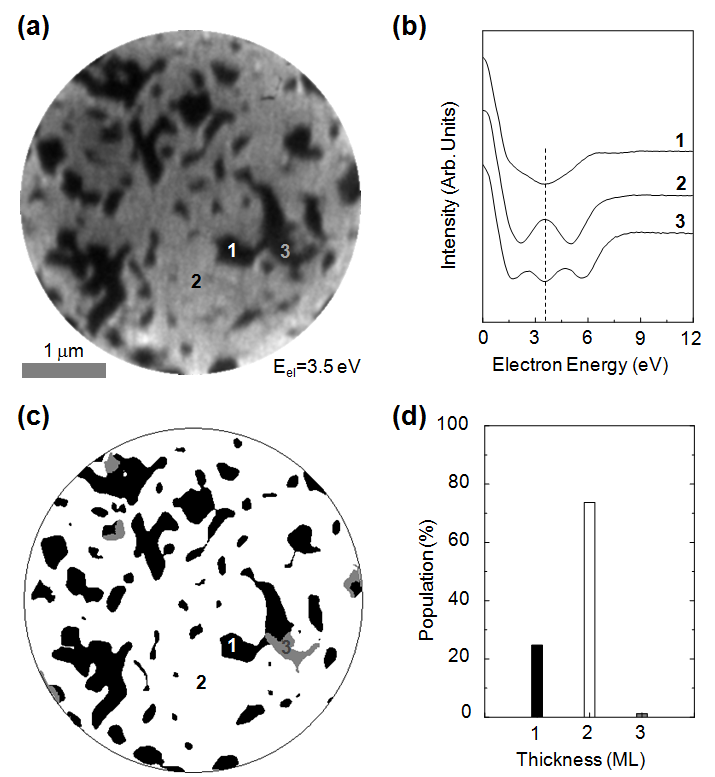
The surface morphology was monitored in situ during the sample growth by LEEM at the National Center for Electron Microscopy at Lawrence Berkeley National Laboratory. The thickness of fabricated graphene samples was determined by LEEM measurements performed at room temperature following the standard procedure David ; Ohta2 . In particular, the electron reflectivity versus kinetic energy curve varies significantly with the number of graphene layers providing position-dependent measurements on the number of graphene layers. A typical bright field image for double layer graphene is shown in Fig. 1(a) over 4 m4 m range, recorded with electron beam of kinetic energy 3.5 eV denoted as the dashed line in Fig. 1(b). In order to determine the number of graphene layers at each position, the electron reflectivity is plotted as a function of electron kinetic energy, as shown in Fig. 1(b), where the number of dips is the same as the number of graphene layers. Regions 1, 2, and 3 in Fig. 1(a) show 1, 2, and 3 dips, respectively, corresponding to single-, double-, or triple-layer graphene, respectively. These regions are painted in black, white, and grey, respectively, in Fig. 1(c). The fractions of regions in the sample covered by different numbers of graphene layers were determined from the areal fractions of differently colored regions in Fig. 1(c). In particular, we find that the double-layer graphene sample contains 74 % of double-layer and 22 % of single-layer graphene.
III EXPERIMENT
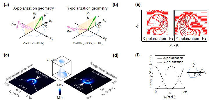
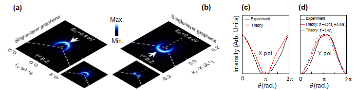
We have performed polarization-dependent ARPES experiments on single- and double-layer graphene at 10 K using a photon energy of 50 eV at beam-lines 10.0.1 and 12.0.1 of Advanced Light Source at Lawrence Berkeley National Laboratory. In Figs. 2(a) and 2(b), we show the typical geometry of ARPES experiments: a beam of monochromatized light with energy and polarization vector is incident on a sample, resulting in the emission of photoelectrons in all directions. The polarization vector of light is referenced with respect to the sample normal. In the experiment presented here, two different geometries were employed as shown in Figs. 2(a) and 2(b). In one geometry shown in Fig. 2(a), the polarization of light is almost parallel to the x axis, while in the other shown in Fig. 2(b) to the y axis; hence, we define these two geometries as X- and Y-polarization, respectively. These geometries have the advantage with respect to the conventional s- and p-polarizations used in previous studies Pescia ; Prince , to measure the whole two-dimensional variation of the intensity maps around a singular (Dirac) point and not just the intensity distributions along two characteristic lines in momentum space. This aspect becomes particularly relevant for some experimental conditions, e. g. , photon energy and sample orientation (i. e. , the mixture of light polarizations), when the intensity maps (or initial electronic states) are neither symmetric nor anti-symmetric with respect to the reflection plane. Under this condition in fact, the conventional notations would not give appropriate information on the symmetry of the initial states.
Figures 2(c) and 2(d) show the experimental photoelectron intensity maps at the Fermi level, , versus the two-dimensional wavevector k for single-layer graphene, for the two polarization geometries. Here, is 0.4 eV above the Dirac point energy, Zhou ; David ; Seyller . The main feature in the intensity maps of both geometries is an almost circular Fermi surface centered at the K point as shown in Figs. 2(c) and 2(d), as expected for a conical dispersion. This is in good agreement with a recent polarization-dependent ARPES study on single-layer graphene when using photons with energy lower than 52 eV Gierz . Surprisingly we find that the the angular intensity distribution is quite different for the two polarizations: for the X-polarization geometry, the minimum intensity position is in the first Brillouin zone, whereas for the Y-polarization geometry, the maximum intensity position is in the first Brillouin zone, suggesting a rotation of the maximum intensity in the - plane around the K point upon rotating the light polarization by , from X to Y (see the white arrows).
The exact rotation angle is extracted from the direct comparison between the raw momentum distribution curves (MDCs) in Fig. 2(e) and the angular dependence of the photoelectron intensity maps integrated over the radial direction around the K point in Fig. 2(f). There is an overall shift of the intensity maxima (minima) by upon changing the light polarization from X (black solid line) to Y (black dashed line), although the latter appears to be slightly shifted by with respect to . As we will show later, this is due to the presence of a finite polarization component along the direction in our experimental geometry.
We note that not only the angular position of the intensity maximum, but also the absolute value of it changes upon changing light polarization. The maximum intensity ratio from experiments is X-polarized/Y-polarized=21.4. However, this number itself is not very meaningful, because the measured ARPES intensity is affected by the difference in the experimental geometries for X- and Y-polarized lights (the difference in the out-of-plane component of light polarization, photon flux per unit area, etc., which are the factors that cannot be controlled to be the same in different experimental geometries). On the other hand, the ratio from our theory that will be discussed later provides X-polarized/Y-polarized=0.83, assuming that the experimental parameters for two geometries are the same except for the in-plane light polarization.
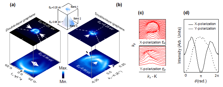
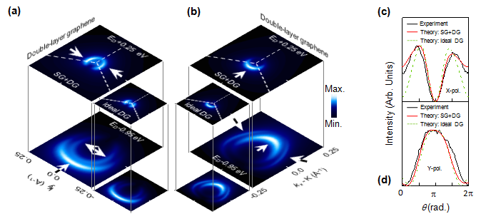
A similar study on Bernal stacked double-layer graphene reveals a strong and complicated momentum-, band-, and polarization-dependence as shown in Figs. 3(a) and 3(b), that is qualitatively different from that of single-layer graphene. Like single-layer graphene, the double-layer sample is slightly doped Seyller , therefore, only three of the four bands are occupied and hence detectable with ARPES as shown in the cartoon of Fig. 3(a). The most prominent feature is that, when the light polarization is changed from X to Y, the maximum intensity positions around the K point in the - plane are rotated by (see white arrows at ). This is in striking contrast with the single-layer case where the rotation is as seen from the raw MDCs in Fig. 3(c) and the photoelectron intensity maps integrated over the radial direction around the K point shown in Fig. 3(d). Due to trigonal warping effects Antonio , however, the rotation for higher-energy states is not exactly as shown in Figs. 3(a) and 3(b).
IV Theoretical analysis
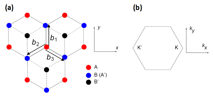
To the best of our knowledge, the only models in the literature describing the polarization-dependence of the ARPES intensity in graphite Himpsel and graphene Eli are substantially different from our results. Previous studies, in fact, predict a small polarization-dependence Himpsel and no polarization-dependence Eli of the photoelectron intensity maps, respectively. Therefore, to be able to reproduce our experimental findings and understand what lies behind this nontrivial polarization dependence, we have developed a new model. In particular, we first consider the Hamiltonian using the tight-binding model based on the orbital of each carbon atom using two parameters: and for the in-plane nearest-neighbor (A-B or A′-B′) and the inter-layer vertical (B-A′) hopping integrals, respectively, as schematically drawn in Fig. 4(a). The parameters and correspond to and , respectively, in the well-known Slonczewski-Weiss-McClure (SWMc) model SWMc1 ; SWMc2 . In our calculation, we have used eV and eV, which are the values in Table II of Grüneis et al. Gruneis , but we do not fix the signs of them. Note that all four possible choices of the signs give exactly the same electron energy band structure within this two-parameter tight-binding model.
With this setup, the tight-binding Hamiltonian of a double-layer graphene for two-dimensional wave vector using a basis set composed of Bloch sums of localized orbitals on each of the four sublattices (A, B, A′, and B′) reads
| (1) |
Here,
| (2) |
with ’s defined as in Fig. 4(a), and
| (3) |
| (4) |
etc. We note that often the k dependence of the basis function is suppressed in the spinor notation for simplicity. In Eq. (1), we have considered a phase difference arising from the finite inter-layer distance d and the perpendicular component of electron wave vector . Here, is not part of the Bloch momentum, but the component of the photoelectron wave vector, which is determined by the photon energy. This quantity plays a crucial role in determining the ARPES intensity of double-layer graphene as will be discussed later and also of multi-layer graphene as previously reported OhtaPRL .
The additional interaction Hamiltonian coupling to electromagnetic waves of wavevector Q for a double-layer graphene can be obtained by using the velocity operator , where in the k-representation and is the Planck’s constant, as Yu [e is the charge of an electron, c is the speed of light, and the external vector potential is given by ] Louie , i. e. ,
| (5) |
The transition matrix elements in Eq. (5) are those taken between basis functions of Bloch sums of orbitals of wavevectors and k. Equation (5) is valid when is much larger than the distance between the nearest-neighbor atoms , i. e. , when the variation in over a length scale of b is much smaller than itself. We shall eventually take the limit in our discussion because the momentum of light is negligible for photon energies considered.
For single-layer graphene, performing a similar type of analysis, we obtain
| (6) |
and
| (7) |
is critical to explain the polarization dependence of , because it describes the interaction between electrons and photons. The lack of polarization dependence in previous studies Himpsel ; Eli is indeed due to the way in which is incorrectly treated. In one case Eli , the light interaction is completely neglected by setting , while in the earlier study on graphite Himpsel , the velocity operator is replaced by the momentum , where is the Planck’s constant and the free-electron mass. This replacement works Starace ; Louie only when the Hamiltonian is local, whereas a tight-binding Hamiltonian, which has been used in the previous studies Himpsel ; Eli as well as our study, is intrinsically non local. The experimental finding of a strong polarization dependence of in Figs. 2 and 3 clearly shows the need for a more complete theoretical treatment. We have developed a theory using the widely adopted tight binding model with one -like localized orbital per carbon atom, but employing the appropriate interaction Hamiltonian with the velocity operator. A very good agreement between our model and the experimental results is obtained for all polarizations and for both single- and double-layer graphene, when we compare Fig. 2 with Fig. 5 and Fig. 3 with Fig. 6 as will be discussed later.
In order to understand what lies behind the observed non-trivial and unexpected wavevector-dependent photoelectron intensity , we need to calculate the absolute square of the transition matrix element , where is a single- or double-layer graphene eigenstate with the band index, is the plane-wave final state projected onto the orbitals of graphene [both and are expressed using the basis set of Bloch sums of localized orbitals at sublattices A and B in Fig. 5(a)] and Yu , which should not be neglected in photoemission process Eli . The use of a projection of the final plane-wave state onto the Bloch sum, which – when using plane-waves basis – is effectively composed of multiple plane-waves CH , allow to explain the non-trivial polarization dependence of the ARPES intensity distribution in Figs. 2(c) and 2(d). Since the polarization of A is in the x-y plane, the projection of onto the -states of graphene will result in zero contribution to the transition matrix elements and hence are neglected in this analysis. For simplicity of notation, and without any loss of generality, in the rest of this section, we shall take the limit of and denote and . For single-layer graphene, we may use
| (8) |
and for double-layer graphene
| (9) |
For photons (with energy eV) used in the experiment, of the planewave final state is much larger than the variation of two-dimensional Bloch wavevector k around a single Dirac point, leading to only a small variation in with any change in k around a single Dirac point. For light with a nonzero polarization component along the z direction, it will only give rise to an additive isotropic term to the photoelectron intensity that is independent of the in-plane polarization of the light.
Now, let us consider the case where k is very close to the Dirac point K as shown in Fig. 4(b), and define (). According to Eq. (2),
| (10) |
where a is the lattice parameter. For single-layer graphene, therefore,
| (11) |
and
| (12) |
where and are the Pauli matrices. The energy eigenvalue and wavefunction of Eq. (11) are given by and
| (13) |
respectively, when is the angle between q and the direction. Using Eqs. (8), (12), and (13), the transition matrix element is given for light polarized along the x direction by
| (14) |
It follows that for (states above the Dirac point energy),
| (15) |
and
| (16) |
with and , respectively.
Similarly, for light polarized along the y direction, the transition matrix element is given by
| (17) |
It follows that for (states above the Dirac point energy),
| (18) |
and
| (19) |
with and , respectively.
In both cases, we can explain the rotation of the intensity maximum in the photoelectron intensity map around the K point by upon the change from X- to Y-polarized light. Comparing Eqs. (15) and (16) with Eqs. (18) and (19), irrespective of the sign of , the maxima of the photoemission intensity map of single-layer graphene is rotated by when the light polarization is rotated by , in agreement with experiment shown in Fig. 2. Moreover, the theoretical results with shown in Figs. 5(a) and 5(b) agree with the measured angular spectral intensity shown in Figs. 2(c) and 2(d); especially, the choice of eV (fitted to previous experiments Gruneis ) reproduces quite well the salient features in the experimentally measured intensity maps.
This is even more clear from the angular dependence of theoretical photoelectron intensity drawn with the red solid lines compared to experimental results drawn with the black solid lines in Figs. 5(c) and 5(d) . Note that experimental intensity maximum for Y-polarized light shows additional shift by in Fig. 2(f). This additional shift is well understood by a finite polarization component along the direction. When we assume the actual light polarization used in the experiment shown in Fig. 2(b), the theoretical intensity exactly matches with the experimental result. On the other hand, when we assume the ideal Y-polarization, the intensity maximum appears at as shown with the blue dashed line in in Fig. 5(d). Therefore, we determine through experiment that the inter-orbital hopping matrix element between two in-plane nearest-neighbor carbon orbitals is negative; we will come back to this point later.
Recent theoretical study on the matrix element in single-layer graphene Gierz has found that, in order to describe the matrix element for Y-polarized light from first-principles calculations using plane-wave basis, one needs multiple plane-wave components for the final photo-emitted electron state. Since we consider a projection of the final state onto the Bloch sum, which – when using the plane-waves basis – is effectively composed of multiple plane-waves CH , our approach can explain the non-trivial polarization dependence of the ARPES intensity distribution in Figs. 2(c) and 2(d). Additionally, our result obtained by using photons with energy 50 eV is in good agreement with the recent study Gierz based on first-principles calculations using photons with energy lower than 52 eV. This suggests that, at photon energy below 52 eV and only when the correct interaction Hamiltonian is employed, the projection of the final state onto the tight-binding Bloch sum may describe the true final state qualitatively. However, since our theoretical framework is within tight-binding formulation, and not from first-principles calculations with plane-wave basis, convergence tests with respect to the number of plane-waves and the character of the true final state are beyond the scope of this paper and, in fact, has been done in a recent study Gierz .
In the case of double-layer graphene, for simplicity of the analysis, we confine our discussion to the inner parabolic bands (bands 1 and 2 in the cartoon in Fig. 3), although we considered all the four bands in our theoretical calculations shown in Figs. 6(a) and 6(b). In double-layer graphene, for electronic states with energy of the Hamiltonian in Eq. (1), the energy and wavefunction are given by where and
| (20) |
respectively Ando:bilayer . The phase difference between the two graphene layers in Eq. (1) appears here as well. Using Eqs. (5), (9), and (20), the transition matrix element is given for light polarized along the x direction by
| (21) |
It follows that for (states above the Dirac point energy),
| (22) |
and
| (23) |
with and , respectively. The perpendicular component of the wavevector reads Shuyun ,
| (24) |
where is the kinetic energy of the photo-electron and the inner potential. Note here that k is a two-dimensional Bloch wavevector, i, e. , it has no out-of-plane component. The inner potential has been measured for graphite by analyzing the energy dispersion at normal emission (i. e. , ) Shuyun . According to Eq. (24), .
Similarly, for light polarized in the y direction, the transition matrix element for a double-layer graphene is given by
| (25) |
It follows that for (states above the Dirac point energy),
| (26) |
and
| (27) |
with and , respectively.
In both cases, we can explain the rotation of the intensity maximum in the photoelectron intensity map around the K point by upon the change from X- to Y-polarized light. Comparing Eqs. (22) and (23) with Eqs. (26) and (27), irrespective of the sign of , the maxima of the photoemission intensity map of a double-layer graphene is rotated by when the light polarization is rotated by , in agreement with experiment shown in Fig. 3. If we assume that , which is qualitatively in agreement with experiment shown in Figs. 3(a) and 3(b), and for the upper band (). Therefore, we have determined that the vertical inter-layer hopping matrix element between two carbon orbitals sitting on top of each other is positive; we will come back to this point later.
Although this model can overall account for the experimental data of double-layer graphene, there is a discrepancy: the measured photoemission intensity at eV along the direction for the X-polarization geometry is finite, whereas the theory predicts this value to vanish as shown in the eV map of the Ideal DG in Fig. 6(a). We believe that this discrepancy arises from the finite size of the light beam spot (8040 m2) which covers not only the double-layer graphene portion but also some single-layer graphene, as discussed in Fig. 1. In fact, double-layer graphene samples inevitably contain a finite amount of single-layer graphene David ; Ohta2 . The fraction of single-layer coverage can be obtained by LEEM measurements David ; Ohta2 : from this analysis shown in Fig. 1, we find that the double-layer graphene sample used here contains 74% double-layer and 22% single-layer graphene. When the theoretical photoelectron intensity maps of single- and double-layer graphene are correspondingly weighted and averaged, the results denoted by SGDG in Figs. 6(a) and 6(b) are in excellent agreement with the experimental data shown in Figs. 3(a) and 3(b). This is even more clear from the angular dependence of the photoelectron intensity maps shown in the red solid lines in Fig. 6(c) and 6(d). Note that the presence of single-layer graphene does not affect the results for the Y-polarization, which is obvious when we compare the red solid and green dashed lines in Fig. 6(d), because both the intensity maxima of single- and double-layer graphene occur near = .
V Discussion
V.1 Berry’s phase
We have shown that, when the light polarization is rotated by , the maximum intensity position in in the - plane of single- and double-layer graphene is rotated by , where and for single- and double-layer graphene, respectively. The physical meaning of these rotations, whose origins rests on the phase factor of the sublattice amplitude of the wavefunctions Antonio , becomes clear upon a complete circulation of q around the Dirac point K (), which directly gives a Berry’s phase Antonio . Recently the Berry’s phase interpretation of McCann ; Zhang ; Novoselov has been given by a different interpretation in terms of pseudospin winding number Parkcond .
The fact that enters in in the form of either or with some constant , demonstrates that the matrix elements directly contain information on the Berry’s phase. The rotation of light polarization gives an additional phase to the phase factor, i. e. , . Thus, the photoelectron intensity is modified accordingly from or upon the rotation of light polarization by , i. e. , the rotation of . This prediction is exactly realized in our experimental results.
The power of our method is that it can be extended in a straightforward way to other materials with Berry’s phase (not necessarily or ). In this case, the photoemission intensities for X- and Y-polarization geometries are given by and , where is a system-dependent constant. The important feature is that the rotation of light polarization by results in a rotation of intensity maxima by for a system with regardless of the constant . Thus, we have demonstrated here that the Berry’s phase can directly be measured from polarization-dependent ARPES.
Unlike methods based on magneto-transport experiments Zhang ; Novoselov , our new method has three important advantages. (i) The Berry’s phase of a specific electronic band can be measured, because ARPES has the angle-resolving power and also because one can set up a tight-binding Hamiltonian focussing on only the electronic states of interest: those two results can directly be compared with each other. (ii) Due to the angle-resolving power, the measured result is free from valley degeneracy for the case of graphene. (iii) Our method does not need electric gating, which is essential for the transport measurements.
V.2 The sign of inter-orbital hopping integrals
Another important finding of our study is that we can directly extract, for the first time, the sign and the absolute magnitude of the inter-orbital hopping integrals (IOHIs) between non-equivalent localized orbitals of a tight-binding Hamiltonian from experiment. Until now, in fact, the sign determination of an IOHI has resorted no to any experimental method, but to ab initio calculations, e. g. , using maximally localized Wannier functions Marzari . In order to understand an ambiguity related with the experimental sign determination, we take the simplest one-dimensional example, and extend the discussion to a more complicated tight-binding model of graphitic systems than the one described previously. We consider simple tight-binding models having s-like localized states, the values of which are all positive in real space (we can arbitrarily set this gauge without losing generality.) If there is only one localized orbital per unit cell in a one-dimensional tight-binding model as drawn in Fig. 7(a), the energy bandstructure varies with the sign of the IOHI as shown in Fig. 7(b). Hence, the sign of IOHIs between “equivalent” orbitals can always be trivially determined Hasan .
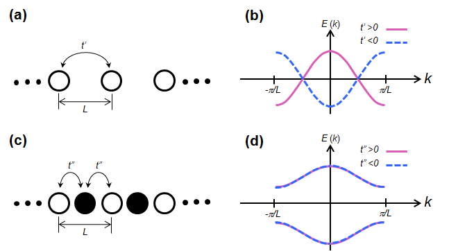
However, if we consider the case where there are two non-equivalent localized orbitals and whose value in real space is positive and if we denote the IOHI between the nearest neighboring orbitals by as drawn in Fig. 7(c), the actual band structure is invariant when we change the sign of as shown in Fig. 7(d). Therefore, even when the actual electronic band structure is empirically determined, the sign of cannot be determined. In general, an empirical tight-binding model with more than one orbital per unit cell has this sign ambiguity problem for IOHIs between “non-equivalent” orbitals, thus preventing an experimental measurement of IOHI from just the energy band dispersions.
We could understand this degeneracy as follows. If we denote the Bloch sums of the two localized orbitals by and , the tight-binding Hamiltonian using this basis set reads
| (28) |
Note here that the matrix elements , in which , involve not only the on-site or nearest-neighbor hopping processes but also all the other possible hopping processes. Now, it is obvious that the following Hamiltonian has exactly the same eigenvalues as :
| (29) |
What we have done by going from to is to change the sign of the IOHI between the two non-equivalent localized orbitals. In fact, the two matrices and are related by a unitary transform, which does not change the eigenvalues of a matrix, with
| (30) |
On the other hand, if we change the signs of the diagonal matrix elements , in which , we get a different eigenvalue spectrum. Thus, there is no ambiguity in the sign of the IOHI between equivalent orbitals. This simple example illustrates that one cannot determine the signs of the IOHIs between non-equivalent orbitals just by looking at the measured electron energy bandstructure.
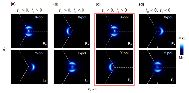
The tight-binding model for double-layer graphene that we used in our calculations is based on the orbitals of carbon atoms with two parameters: and for the nearest-neighbor in-plane and the vertical inter-layer hopping integrals, respectively. The parameters and correspond to and in the well-known Slonczewski-Weiss-McClure model, respectively SWMc1 ; SWMc2 , and we have used eV and eV Gruneis . The photoemission intensity map in the - plane is strongly dependent on the signs of both and as shown in Fig. 8. Because the four different choices of the signs produce exactly the same electronic band structure, it has not been known from experiments which choice of the signs of the IOHIs is physically correct, although the absolute values have been experimentally estimated Dresselhaus1 ; Dresselhaus2 .
This sign-ambiguity problem still exists even when we include more complicated hopping processes in the model, especially the non-vertical inter-layer hopping integrals and , there still exist unitary transforms that leave the energy eigenvalues unchanged. In a tight-binding model having four hopping integrals (, , , and ), the following four different sets of parameters give exactly the same electron energy bandstructure: (, , , ), (, , , ), (, , , ), and (, , , ), assuming that the first set is composed of the values currently accepted and used when the SWMc model is considered. In principle, there should be eight different sets of parameters giving the same energy bandstructure; however, from our knowledge that the nearest-neighbor intralayer hopping integrals in different graphene layers are the same, we have reduced the number of candidates to four. This is also the reason why we considered only the four cases in Fig. 8.
We have shown that the choice of and , i. e. , and in Fig. 8(c), reproduces the experimental results shown in Figs. 3(a) and 3(b), thus experimentally determined the signs of these IOHIs. The signs of the IOHIs used for graphite in the conventional model SWMc1 ; SWMc2 is indeed correct. Previous theoretical study has also tried to determine the signs Eli , but inappropriate theoretical approaches (as previously mentioned) and the lack of full polarization-dependent experimental data have led to incorrect speculations, which do not agree with the conventional model SWMc1 ; SWMc2 as well as our results. Our method can generally be used to determine the sign of the hopping integrals in complicated materials such as cuprates as well as in simple materials such as gallium arsenide and one-dimensional crystals having two atoms per unit cell.
VI Summary
We have shown that ARPES can be used as a powerful tool to directly measure quantum phases such as the Berry’s phase of a specific electronic band in graphene with advantages compared to the interference type of measurements Swerner ; Tomita ; Bitter which do not give any information on the band-specific Berry’s phase, and the sign of the hopping integral between non-equivalent orbitals, never measured for any material before. The experimental and theoretical procedures developed here can be applied in studying the electronic, transport, and quantum interference properties of a huge variety of materials.
Acknowledgements.
We gratefully acknowledge D.-H. Lee, J. Graf, C. M. Jozwiak, S. Y. Zhou and H. Zhai for helpful discussions. This work was supported by the Director, Office of Science, Office of Basic Energy Sciences, Materials Sciences and Engineering Division, of the U.S. Department of Energy under Contract No. DE-AC02-05CH11231.References
- (1) A. Bohm, A. Mostafazadeh, H. Koizumi, Q. Niu, and J. Zwanziger The Geometric Phase in Quantum Systems (Springer-Verlag, Berlin Heidelberg, 2003).
- (2) Y. Aharonov and D. Bohm, Phys. Rev 115, 485 (1959).
- (3) E. McCann and V. I. Fal’ko, Phys. Rev. Lett. 96, 086805 (2006).
- (4) Y. Zhang, Y. -W. Tan, H. L. Stormer, and P. Kim, Nature 438, 201 (2005).
- (5) K. S. Novoselov, E. McCann, S. V. Morozov, V. I. Fal’ko, M. I. Katsnelson, U. Zeitler, D. Jiang, F. Schedin, and A. K. Geim, Nature Phys. 2, 177 (2006).
- (6) Y. Taguchi, Y. Oohara, H. Yoshizawa, N. Nagaosa, and Y. Tokura, Science 291, 2573 (2001), and references therein.
- (7) S. Murakami and N. Nagaosa, Phys. Rev. Lett. 90, 057002 (2003).
- (8) D. Hsieh et al., Science 323, 919 (2009).
- (9) A. Grüneis et al., Phys. Rev. B 78, 205425 (2008).
- (10) N. Marzari and D. Vanderbilt, Phys. Rev. B 56, 12847 (1997).
- (11) J. C. Slonczewski and P. R. Weiss, Phys. Rev. 109, 272 (1958).
- (12) J. W. McClure, Phys. Rev. 108, 612 (1957).
- (13) S. -W. Yu et al., Surf. Sci. 416, 396 (1998).
- (14) E. L. Shirley, L. J. Terminello, A. Santoni, and F. J. Himpsel, Phys. Rev. B 51, 13614 (1995).
- (15) M. Mucha-Kruczyński et al., Phys. Rev. B 77, 195403 (2008).
- (16) E. Rollings et al., J. Phys. Chem. Solids 67, 2172 (2006).
- (17) D. A. Siegel et al., Appl. Phys. Lett. 93, 243119 (2008).
- (18) T. Ohta et al., New J. Phys. 10, 023034 (2008).
- (19) D. Pescia, A. R. Law, M. T. Johnson, and H. P. Hughes, Solid State Commun. 56, 809 (1985).
- (20) K. C. Prince, M. Surman, Th. Lindner, and A. M. Bradshaw, Solid State Commun. 59, 71 (1986).
- (21) S. Y. Zhou et al., Nature Mater. 6, 770 (2007).
- (22) Th. Seyller, K. V. Emtsev, F. Speck, K. -Y. Gao, and L. Ley, Appl. Phys. Lett. 88, 242103 (2006).
- (23) I. Gierz, J. Henk, H. Höchst, C. R. Ast, and K. Kern, Phys. Rev. B 83, 121408(R) (2011).
- (24) A. H. Castro Neto, F. Guinea, N. M. R. Peres, K. S. Novoselov, and A. K. Geim, Rev. Mod. Phys. 81, 109 (2009).
- (25) T. Ohta et al., Phys. Rev. Lett. 98, 206802 (2007).
- (26) P. Y. Yu and M. Cardona, Fundamentals of Semiconductors: Physics and Materials Properties; Springer-Verlag: Berlin Heidelberg, 1999.
- (27) A. F. Starace Phys. Rev. A 3, 1242 (1971).
- (28) S. Ismail-Beigi, E. K. Chang, and S. G. Louie, Phys. Rev. Lett. 87, 087402 (2001).
- (29) C. -H. Park and S. G. Louie, Nano Lett. 9, 1793 (2009).
- (30) Ando, T. J. Phys. Soc. Jpn. 2007, 76, 104711.
- (31) Zhou, S. Y.; Gweon, G. -H.; Lanzara, A. Ann. Phys. 2006, 321, 1730-1746.
- (32) C. -H. Park and N. Marzari, arXiv:1105.1159v4.
- (33) M. Z. Hasan et al., Phys. Rev. Lett. 92, 246402 (2004).
- (34) W. W. Toy, M. S. Dresselhaus, and G. Dresselhaus, Phys. Rev. B 15, 4077 (1977).
- (35) A. Misu, E. E. Mendez, and M. S. Dresselhaus, J. Phys. Soc. Jap. 47, 199 (1979).
- (36) S. A. Werner, R. Colella, A. W. Overhauser, and C. F. Eagen, Phys. Rev. Lett. 35, 1053 (1975).
- (37) A. Tomita and R. Y. Chiao, Phys. Rev. Lett. 57, 937 (1986).
- (38) T. Bitter and D. Dubbers, Phys. Rev. Lett. 59, 251 (1987).