Ultra-low carrier concentration and surface dominant transport in Sb-doped Bi2Se3 topological insulator nanoribbons
Abstract
A topological insulator is a new state of matter, possessing gapless spin-locking surface states across the bulk band gap which has created new opportunities from novel electronics to energy conversion. However, the large concentration of bulk residual carriers has been a major challenge for revealing the property of the topological surface state via electron transport measurement. Here we report surface state dominated transport in Sb-doped Bi2Se3 nanoribbons with very low bulk electron concentrations. In the nanoribbons with sub-10nm thickness protected by a ZnO layer, we demonstrate complete control of their top and bottom surfaces near the Dirac point, achieving the lowest carrier concentration of 2×1011cm-2 reported in three-dimensional (3D) topological insulators. The Sb-doped Bi2Se3 nanostructures provide an attractive materials platform to study fundamental physics in topological insulators, as well as future applications.
The exotic electronic properties of the surface state, due to its spin-momentum locked Dirac cone in the electronic band structure, define a topological insulator as a new class of quantum matterMoore2010 ; Qi2010 ; Hasan2010 ; Fu2007 ; Konig2007 . Moreover, it is predicted to offer exciting physics in condensed matter systems, such as elusive quasi-particles, spin transport, and fault tolerant quantum information processingQi2010 ; Hasan2010 ; Fu2007 ; Konig2007 ; Qi2009 ; Seradjeh2009 ; Fu2008 . Bismuth selenide (Bi2Se3) and its relative compounds are one of the most promising candidates to realize the ideal three-dimensional topological insulator due to their large bulk band gap and simple surface band structureZhang2009 . There have been significant advances to probe the surface state in these materials by various methods, such as angle-resolved photoemission spectroscopy (ARPES)Xia2009 ; Chen2009 ; Zhang2010 and scanning tunneling microscopy (STM)Roushan2009 ; Alpichshev2010 ; Hanaguri2010 . Transport measurements in bulk crystals have demonstrated the existence of these surface states as wellAnalytis2010 ; Qu2010 ; Taskin2011 .

Nanoscale topological insulator devices offer a unique opportunity to study the surface state as the surface to volume ratio is increased to manifest the surface effectPeng2009 ; Xiu2011 . Moreover, on mesoscopic length scale, one can study transport reflecting the fundamental nature of carriers, as shown in previous cases like grapheneZhang2005 ; Novoselov2005 . However, in the case of topological insulators, material imperfection issues in the bulk blur surface state signatures and limit further in-depth transport studies. One of the critical obstacles is the dominant bulk electrons outnumbering surface state electronsCheckelsky2010 ; Steinberg2011 ; Kim2011 ; Kong2011 . Moreover, the material is very sensitive to environmental contamination as sample degradation by environmental exposure has been observed in a few studiesAnalytis2010 ; Kong2011ACS . Here, we report Sb doping for Bi2Se3 nanoribbons to suppress the bulk conductivity and achieve surface state dominant transport in nanodevices. Transport experiments confirm the significant suppression of the bulk contribution without degradation of electron mobility. In addition, we deposit an oxide layer on top of the nanoribbons as a protective layer, which enables ultralow carrier concentration controllable near the Dirac point and helps realize surface dominant transport in the topological insulator nanostructures.
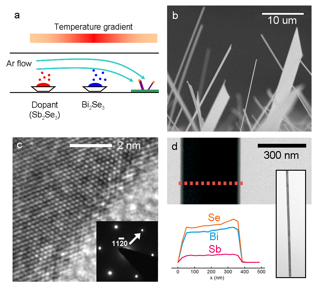
To suppress the bulk conductivity in topological insulator nanoribbons, we synthesize Bi2Se3 nanoribbons with Sb doping. Sb is known as an effective compensation dopant to reduce bulk electron density to 1017cm-3 and does not destroy the topological surface stateAnalytis2010 ; Zhang2010APL . Bi2Se3 nanoribbons are synthesized via vapor-liquid-solid growth mechanism using gold particles as catalystsPeng2009 ; Kong2010 , and Sb vapor is introduced from a Sb2Se3 source material placed at the lower temperature zone (Fig. 1a). As-grown ribbons are 100-300nm thick, their widths vary from 200nm to several micrometers, and their lengths are up to tens of micrometers (Fig. 1b). Sb-doped Bi2Se3 nanoribbons are in a single crystalline rhombohedral phase, which is the same as undoped Bi2Se3 nanoribbons. The distribution of Sb dopants appears to be spatially uniform in the nanoribbon, as confirmed by energy-dispersive X-ray spectroscopy (EDX) (Fig. 1c-1d).
| Sample | Sb | Rsheet | RHall | nHall |
|---|---|---|---|---|
| number | doping | () | () | (1012cm-2) |
| B1 | 0.0% | 43 | -7.4 | 84.5 |
| B2 | 2% | 177 | -14.7 | 42.5 |
| S1 | 3.0% | 422 | -39.9 | 15.7 |
| S2 | 5.5% | 975 | -51 | 12.3 |
| S3 | 7.0% | 1350 | -63.1 | 9.9 |
The Sb doping concentration in Bi2Se3 nanoribbons can be tuned systematically by controlling the temperature of the Sb2Se3 source material. For different Sb doping concentrations, we fabricated nanodevices with Hall bar electrodes to characterize the basic carrier types and densities. The entire set of samples (Table I) shows n-type carrier dominant transport as their Hall resistances are negative values. By introducing more Sb dopants into the ribbon, its sheet resistance increases more than an order of magnitude and the dramatic change in Hall resistance also indicates a much lower carrier density, implying the bulk electron contribution is reduced significantly (Table I). At a high Sb doping concentration (5-7%), the carrier density reaches 1013cm-2. Considering the carrier density of the surface states from both top and bottom surfaces near the bulk conduction band edge is 1013cm-2 Chen2010 , such low carrier density in the Sb-doped nanoribbons suggests that the transport is no longer dominated by large amount of bulk electrons.

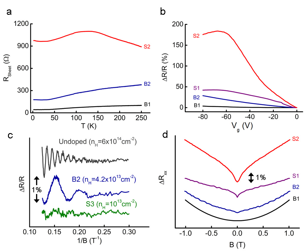
Additional electronic transport studies confirm that the bulk electron contribution is reduced significantly by the Sb doping. In Figure 2a, temperature dependent resistances from low Sb concentration samples (B1, B2) follow typical metallic behavior. In contrast, for the sample of high Sb concentration (S2), the resistance starts to increase and saturates at low temperature. An increase in resistance upon reducing temperature is likely due to freezing out of the bulk carriers. Moreover, electrostatic gating experiments in field effect transistor devices manifest drastic difference between low Sb concentration samples and high Sb concentration samples (Fig. 2b). Low Sb-doped samples (B1, B2) show weak gating dependence by a bottom gate, which is reasonable as the ribbon thicknesses (>100nm) is much larger than the depletion layer thickness (10nm) with still relatively high carrier concentration. However, the gating response becomes larger with increasing Sb doping concentration. The sample with the highest Sb doping (S2) exhibits the largest increase of its resistance, or the most significant decrease in bulk carrier concentration. The conductance of this ribbon decreases by more than half by electrostatic manipulation with the bottom gate in spite of its large thickness (120nm), which strongly suggests the increase of the depletion layer thickness (35nm) and the significant suppression of the bulk transport contribution.
Magnetotransport data clearly shows the emergence of the surface state and suppression of bulk electrons by Sb doping as well. In the high field magnetoresistance (MR), quantum oscillations (SdH oscillations) are observed in samples of different Sb concentrations (Fig. 2c). The oscillation does not depend on the gate voltage (Vg), which suggests that the oscillation originates from bulk electrons. Without Sb doping, the bulk SdH oscillation periodicity in an inverse magnetic field is small. It indicates the cross section of the Fermi surface is large, consistent with high bulk carrier concentration. As Sb concentration increases, the oscillation period gets larger and disappears at the highest doping level. That is, the bulk electron pocket crossing the Fermi level eventually becomes too small so that the oscillation period is too large to be detected in our magnetic field range (8T). The small cross section of the bulk Fermi surface means the contribution of bulk electrons is greatly reduced. In the low magnetic field, weak anti-localization (WAL), the quantum correction which emerges strongly in the spin-orbit coupled surface stateChen2010 , is absent in the MR trace of the undoped sample (Fig. 2d, B1) as the large bulk electron contribution masks surface state transport. On the contrary, higher Sb concentration samples (Fig. 2d, S1, S2) manifest a sharp cusp near zero magnetic field, which is a characteristic feature of WAL. Owing to the reduced bulk electron contribution by Sb doping, all the transport measurements including temperature dependence, field effect gating, and magnetotransport consistently indicate significant contribution from surface state transport.
Even though the 5-7 Sb doping in the aforementioned experiments can effectively reduce the carrier concentration to 1013cm-2 and lower the Fermi level close to the conduction band edge, nanoribbons are still exposed to extrinsic contaminations during device fabrication, which have the issue of the additional increase of the bulk carrier concentration, as reported by previous studiesAnalytis2010 ; Kong2011ACS . Therefore, we hypothesize that the Sb-doped Bi2Se3 should have much lower carrier concentration if protected from the ambient environment. Here we deposit an insulating Zinc Oxide (ZnO) layer on top of the nanoribbons to protect samples from external contamination. The sputtered ZnO layer covers the entire surface of the nanoribbons, which would prevent degradation and extrinsic doping that might happen during the standard fabrication process.

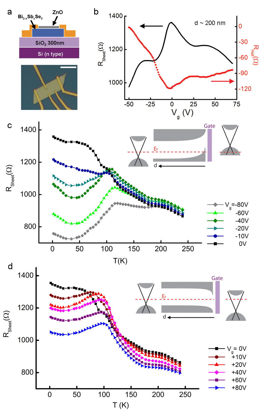
Here we fabricate a bottom-gate device using Sb-doped and ZnO protected Bi2Se3 nanoribbon with a large thickness (200nm), as shown in Fig. 3a, The gating is effective in the range of 30nm for this carrier concentration, and the thickness of the ribbons is much larger than this effective gating layer thickness, so that the electrostatic bottom gate can only affect the bottom surface state. We have studied gate-dependence and temperature-dependence of resistance, which can examine the nature of carriers induced by gating voltage. Owing to the Sb doping and ZnO protective layer as discussed above, we found that the Fermi level of the bottom surface in this particular device is close to the Dirac point. In Figure 3b, its resistance decreases by either direction of gating voltage, and Hall resistance increases as more electronic states on the bottom surface (p-type carriers for negative Vg and n-type carriers for positive Vg) are populated. At zero Vg, resistance increases with decreasing temperature, and saturates at low temperature, similar to the case of Sb-doped bulk crystalAnalytis2010 . The increase of resistance at high temperature (T >100K) can be understood as the freeze out of the thermally populated bulk electronic states. As p-type carriers are induced by the negative Vg (Fig. 3c), there is a noticeable change in the temperature curve - resistance starts to drop down by cooling. As we have observed this metallic temperature dependence when the Fermi level is crossing the bulk band, we conclude that it becomes a mixed state with bulk carriers as increasing p-type carriers. On the other hand, the temperature curve does not change qualitatively by inducing more n-type carriers (positive Vg, Fig. 3d).
The asymmetric trends in the temperature dependent transport reflect the characteristic band structure near the Dirac point in Bi2Se3 topological insulators. From ARPES studiesXia2009 ; Analytis2010PRB , the Dirac point of surface states is just above the bulk valance band edge, while it is relatively far apart from the bulk conduction band edge (0.2eV). Therefore, within our Vg range (+80V), positive gating only creates more electrons from the surface band but not from the bulk band, which will not change the overall shape of the temperature curve. In contrast, bulk electronic states are easily populated from the valence band by negative gating. Now, the ribbon is in the mixed state, evolving from surface dominant transport to bulk dominant transport by adding more bulk hole carriers by gating, showing the dramatic change in the temperature-dependent resistance curves. This temperature dependence study clearly shows that we can independently tune the Fermi level of one surface near the Dirac point. This is an interesting system to controllably build either a topological insulator junction of dual types of carriers or a single surface junction to study novel proximity effects in the futureSeradjeh2009 ; Fu2008 .

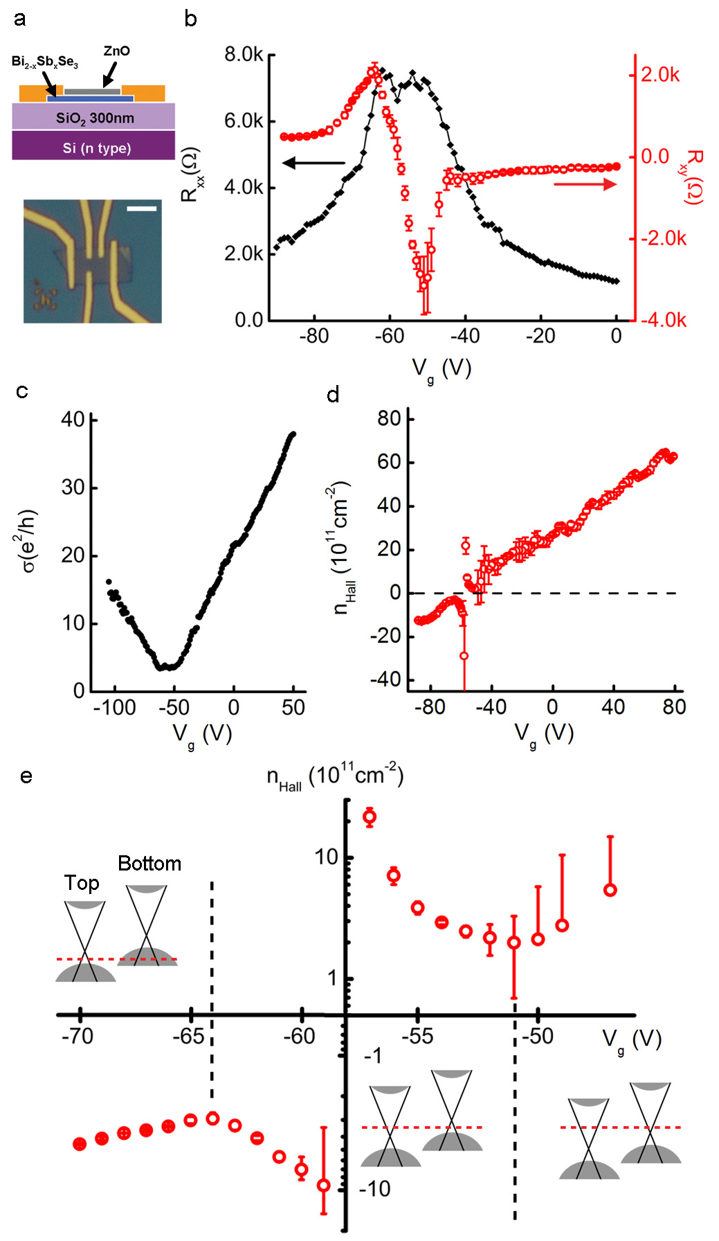
In addition to the manipulation of one surface in the thick ribbons, we eventually want to control the Fermi level of the both top and bottom surfaces to achieve ultralow carrier concentration near the Dirac point. To shift the Fermi level of the entire ribbon together by electrostatic gating, the nanoribbons need to be further thinned down. We etched a thick, Sb-doped ribbon (100nm) by Argon plasma in a sputtering machine and in-situ deposited a 15nm thick ZnO protection layer. In Fig. 4a, the ribbon is semitransparent with a thickness of 6nm (confirmed by AFM), more than 30 times thinner than the previous device (Fig. 3). From this 6nm-thin device, we can achieve very low electron concentration of 2.8×1012cm-2 at zero Vg (Fig. 4b and 4d). Since this concentration value is more than three times lower than that (1013cm-2) of the surface states from the both top and bottom surfaces of which Fermi level is near the bulk conduction band edge, we believe that the Fermi level of the both top and bottom surfaces is completely within the bulk band gap. In other words, the Fermi level crosses only the surface Dirac cone above the Dirac point.
In this ZnO-protected nanoribbon device already with very low carrier concentration, its small thickness of 6nm makes it possible to shift the Fermi level of the entire ribbon by electrostatic gating across the Dirac point. When Vg is changed from positive to negative bias, its longitudinal resistance (Rxx) first increases and reaches a large peak value (7k) at Vg of -50V, and then decreases when further lowering the gating voltages below Vg of -65V (black curve, Fig. 4b). The Hall resistance (red curve, Fig. 4b) changes significantly too, as its magnitude increases by more than 10 times and switches its sign also at Vg of -60V. These results clearly demonstrate the ambipolar field effect and suggest that the entire sample is converted from n-type to p-type. The sample conductance depends on gating voltage linearly, except at the plateau of minimum conductance (3.6G0) (Fig. 4c). The absence of zero conductance region during the ambipolar transition is due to the gapless surface states. The origin of the conductance plateau is not definitive yet, which could be explained as suggested in previous theoretical studiesLiu2010 ; Linder2009 ; Culcer2010 . The carrier density obtained by Hall resistance is plotted in Figure 4d showing its linear dependence on Vg as well. The sample stays pure n-type until Vg = -50V, and then switches to a mixed carrier state (-65V <Vg <-50V) and p-type (Vg <-65V) subsequently (Fig. 4e). Considering the order of low carrier density (<1012 cm-2), now both surfaces are very close to the Dirac point in this range of Vg. In fact, the minimum carrier density obtained from Hall resistance is about 2×1011cm-2, which is 10 times lower than the concentration at zero Vg. This low carrier density value is also comparable with that of initial single layer graphene devicesZhang2005 ; Novoselov2005 .
The Sb doping of topological insulator nanoribbons and the protective oxide layer effectively reduce bulk carriers originating from both intrinsic and extrinsic material defects. Consequently, we are able to carry out electronic transport measurement to demonstrate surface state dominated transport as a result of fairly low bulk carrier concentration. In the thick sample, single surface can be individually tuned within the wide range of the Fermi level. In the thin sample, both top and bottom surfaces are easily tunable across the Dirac point by electrostatic gating. With minimal contribution from residual bulk carriers, Sb-doped Bi2Se3 nanoribbons will offer a great opportunity to test various topological insulator phenomena proposed by theory, as well as be the optimal material for future applications.
.1 Acknowledgments
Acknowledgements.
We thank K. Lai and J. R. Williams for the helpful discussions, and B. Weil for the help in the manuscript preparation. Y.C. acknowledges the supports from the Keck Foundation, DARPA MESO project (N66001-11-1-4105), and King Abdullah University of Science and Technology (KAUST) Investigator Award (No. KUS-l1-001-12).References
- (1) J. E. Moore, Nature 464, 194 (2010).
- (2) X.-L. Qi, S.-C. Zhang, arXiv:1008.2026 (2010).
- (3) M. Z. Hasan, C. L. Kane, Rev. Mod. Phys. 82, 3045 (2010).
- (4) L. Fu, C. Kane, Phys. Rev. B 76, 04530 (2007).
- (5) M. Konig et al., Science 318, 766 (2007).
- (6) X.-L. Qi, R. Li, J. Zang, S.-C. Zhang, Science 323, 1184 (2009).
- (7) B. Seradjeh, J. E. Moore, M. Franz, Phys. Rev. Lett. 103, 066402 (2009).
- (8) L. Fu, C. Kane, Phys. Rev. Lett. 100, 096407 (2008).
- (9) H. Zhang et al., Nat Phys 5, 438 (2009).
- (10) Y. Xia et al., Nat Phys 5, 398 (2009).
- (11) Y. L. Chen et al., Science 325, 178 (2009).
- (12) Y. Zhang et al., Nat Phys 6, 584 (2010).
- (13) P. Roushan et al., Nature 460, 1106 (2009).
- (14) Z. Alpichshev et al., Phys. Rev. Lett. 104, 016401 (2010).
- (15) T. Hanaguri et al., Phys. Rev. B 82, 081305 (2010).
- (16) J. G. Analytis et al., Nat Phys 6, 960 (2010).
- (17) D.-X. Qu et al., Science 329, 821 (2010).
- (18) A. A. Taskin et al., Phys. Rev. Lett. 107, 016801 (2011).
- (19) H. Peng et al., Nat Mater 9, 225 (2009).
- (20) F. Xiu et al., Nat Nano 6, 216 (2011).
- (21) Y. Zhang, Y.-W. Tan, H. L. Stormer, P. Kim, Nature 438, 201 (2005).
- (22) K. S. Novoselov et al., Nature 438, 197 (2005).
- (23) J. G. Checkelsky, Y. S. Hor, R. J. Cava, N. P. Ong, Phys. Rev. Lett. 106, 196801 (2011).
- (24) H. Steinberg et al., arXiv:1104.1404 (2011).
- (25) D. Kim et al., arXiv:1105.1410 (2011).
- (26) D. Kong et al., arXiv:1107.0535 (2011).
- (27) D. Kong et al., ACS Nano 5, 4698 (2011).
- (28) Y. Zhang et al., Appl. Phys. Lett. 97, 194102 (2010).
- (29) D. Kong et. al., Nano Lett. 10, 329 (2010).
- (30) J. G. Analytis et al., Phys. Rev. B 81, 205407 (2010).
- (31) J. Chen et al., Phys. Rev. Lett. 105, 176602 (2010).
- (32) C.-X. Liu et al., Phys. Rev. B 81, 041307 (2010).
- (33) J. Linder, T. Yokoyama, A. Sudb , Phys. Rev. B 80, 205401 (2009).
- (34) D. Culcer, E. H. Hwang, T. D. Stanescu, S. Das Sarma, Phys. Rev. B 82, 155457 (2010).