Nature of resonant Raman scattering in ZnCoO films under sub-band excitation
Abstract
Using the methods of scanning electron (SEM) and atom force microscopy (AFM) as well as photoluminescence (PL) and Raman micro-spectroscopy, we investigated films ( and ) grown by molecular beam epitaxy on sapphire substrates. It is found that the films have a nanocrystalline structure with the grain size decreased from down to nm at changing the concentration from to . High-resolution SEM images of film have been interpreted as inhomogeneous lateral distribution of atoms.
Two broad emission bands observed in spectra of band-to-band PL are ascribed to emission from nano-regions enriched and depleted with . In low-temperature PL spectra under sub-band excitation of films, there observed are intra-center optical transitions due to center: , , , , . Offered is a new approach to interpretation of resonant enhancement observed in multi-phonon scattering by phonons in under sub-bandgap excitation combined with the extrinsic Fröhlich interaction mediated via a localized exciton bound to the isoelectronic impurity in which the electron is strongly localized at the magnetic ion. This conclusion is confirmed by the dependence of Raman spectra on the quantum energy of exciting radiation. It assumes formation of intermediated sub-band electron excited states of isoelectron dopant, they are also referred to as charge transfer processes.
1 Introduction
nanostructures with impurities of -metals are promising materials for devices in opto- and nanoelectronics, spintronics as direct-band material with a high width of the forbidden gap ( eV) and high bound energy of excitons at room temperature ( meV) [1].
As it is commonly considered, doping the epitaxial films with transition metals Co or Mn is able to essentially change the local structure of crystalline lattice, which influences on electron and magnetic properties of material. However, up to date the electronic structure of -centers in remains unstudied in detail. It was shown that magnetic properties of -doped films depend on the method of growing [2] and structural defects [3]. Also observed was ferromagnetic ordering in () with the Curie temperature , and it was shown that growth in the charge carrier concentration provides enhanced ferromagnetism [4]. For this case, exchange interaction between magnetic impurities is indirect and realized either via charge carriers [5], or defects and/or impurity electron states with a non-zero spin [6], the magnetization value being essentially dependent on the concentration of free charge carriers and Fermi level position. The -type conductivity in is caused by oxygen vacancies ( ) as well as interstitial ( ) [7]. Therefore, for -type where one can observe carrier-induced ferromagnetism above room temperature [6] with exchange interaction between localized spins of -electrons in the center and electron states of shallow donors with a non-zero spin, offered is the so-called magnetic-polaron model of high-temperature magnetism. However, the energy of magnetic polaron is sufficiently low [8], and, respectively, no quantitative experimental proofs to support the polaron model are found yet. There exist some other theoretical models where ferromagnetic ordering is realized due to inhomogeneous distribution of magnetic impurities in crystalline lattice [9]. Formation of a special network of nano-sized clusters with various -component composition (spinodal component decomposition) can be responsible for ferromagnetic ordering at temperatures higher than the room one [9].
A non-significant difference between ionic radii of and in tetrahedral coordination (ionic radius of is equal to , - ) should promote efficient dissolution of in and cause a weak distortion in crystalline lattice. As recently shown, solubility in the wurtzite matrix sharply increases with lowering the grain sizes of crystallites. There obtained were MBE-grown films with and sizes of crystalline grains [10]. Also synthesized were colloidal wurtzite nanocrystals ( ) with [11]. Observed in solid solutions of wurtzite-type was the effect of spinodal component decomposition and creation of local nano-regions enriched with magnetic impurities [9, 12]. Similar nano-regions with spinodal component decomposition were found in DMS nano-structures ( ) [13]. It was shown that the local nano-regions of spinodal decomposition in the case of DMS nano-structures are considerably less ( ) [14].
The method of Raman scattering is widely used for studying the phonon properties and secondary impurity phases in [15]. The electron structure of defect-ion centers in matrix was investigated using the method of resonant Raman scattering in the only work [16]. In this work, the resonant Raman process under sub-bandgap excitation of polycrystals was explained as based on interaction of phonons with carriers in excited states of -impurity center [16]. In single crystals implanted with hydrogen and nitrogen atoms, the resonant multi-phonon scattering by n-phonons ( ) under sub-bandgap excitation ( ) was interpreted being based on the model for the Fröhlich mechanism of interaction between -phonons and excitons bound with impurities [17]. On the other hand, as it was shown for () semiconductors, magnetic ordering changes the electron band structure, which can be pronounced in resonance effects observed in Raman spectra [18]. As a result, one can observe strong multi-phonon processes in -scattering that are the result of strong electron-phonon interaction related with excitation of -shell in . In Raman spectra of , the lines of scattering in the vicinity and are observed, and these are slowly shifted to and with increasing the applied magnetic field. This resonant amplification of Raman scattering by -phonons with end wave vectors in europium chalcogenides being in ferromagnetic and paramagnetic phases was interpreted with account of Fröelich electron-phonon interaction and availability of spin fluctuations. Up to date, no investigation of resonant Raman scattering in DMS under excitation with energies close to electron transitions with participation of -states was performed.
In this work, we used the complex of analytical methods of AFM and SEM microscopy as well as photoluminescence and Raman micro-spectroscopy to study electron and structure properties of MBE grown -doped films. Especial attention was paid to studying the resonant Raman scattering caused by centers in films with a nano-column structure. It has been shown that detailed analysis of Raman resonance effects in films doped with under sub-bandgap excitation can give information upon electron states of centers and the width of bandgap. Also, we have ascertained a clear dependence between the value (force) of electron-phonon interaction and correlation length that corresponds to diameters of the nano-column structure in films, which are obtained using AFM and SEM structural-morphologic investigations.
2 Experimental details
The films were grown on -sapphire substrates in a Riber Epineat MBE system equipment with conventional effusion cells for elemental and . Atomic oxygen was supplied via an Addon radiofrequency plasma cell equipped with a high-purity quartz cavity. The film thickness was about . X-ray diffraction patterns were used to ascertain the overall structure and phase purity. All positions of the peaks can be readily indexed to the hexagonal wurtzite with lattice constants and for the undoped sample, which matches well with the values of single crystal. After substitution with atom, both - and -axis lattice constants of matrix were increased ( () and () for () at. , respectively). In particular, the () peak located at about is much stronger than the others for all the studied samples, which means that films possess a nano-column structure with preferential orientation along -axis.
Confocal micro-Raman and PL spectra collected by Jobin-Yvon T64000 triple spectrometer, equipped with a CCD detector, were performed using different lines of mixed ion laser ( and ) and - laser ( nm) with output power less than . An Olympus BX41 microscope equipped with a objective possessing at room temperature measurements and a long-focus objective with at low temperatures was used to focus laser light on the sample and collect scattered light into the spectrometer. Spatial resolution (lateral and axial) was about . The temperature dependent micro-Raman and PL spectra were performed using a Linkam THM600 temperature stage and CRYO Industries RC102-CFM helium cryostat. The AFM measurements were performed by a Dimension 3000 Nano-Scope IIIa scanning probe microscope. The chip structure of samples were also studied using a ZEISS EVO-50 scanning electron microscope (SEM).
3 Results and discussion
Shown in Fig. 1 are images of surface with its typical morphology for three studied MBE-grown epitaxial films and their corresponding cross-section of the SEM image. These films possess a nanograin structure of surface morphology with the mean grain size (Figs 1а, 1d).
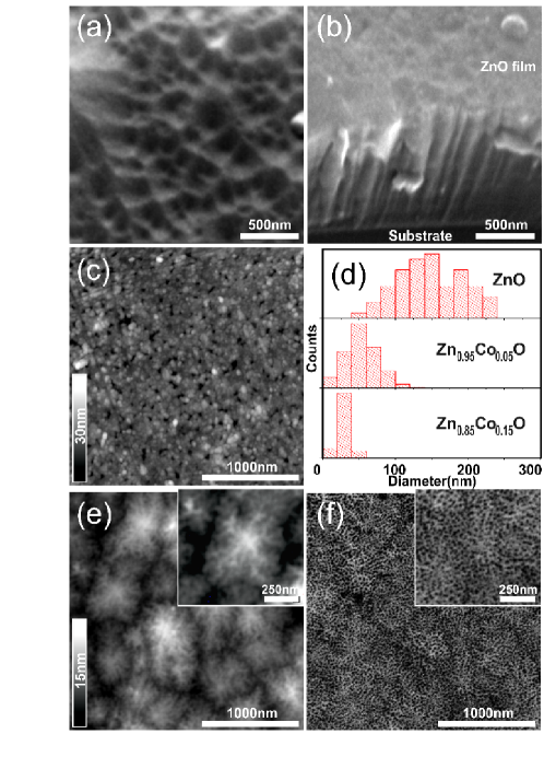
The SEM images near the chipped edge of the studied film show a column-like structure along the growth direction (Fig. 1b). In the case of (Fig. 1c), the main grain size is decreased approximately down to (Fig. 1b) as compared to the undoped sample. In the case of film, a complex structure consisting of large blocks (with the size ) (Fig. 1e), everyone of which possesses a substructure with nano-grains of mean sizes close to (Figs 1d and 1f). In the case of films, we observed a difference between AFM surface morphology and SEM image obtained with high spatial resolution approximately . It is related with the fact that in the SEM image, beside surface relief, considerable contribution is provided by the phase contrast caused by inhomogeneous distribution of atoms in film in the sub-surface of the film with the thickness up to - . The compositional phase contrast is caused by the considerably higher efficiency of electron absorption in atoms as compared with those of matrix (- to -times more). Therefore, it is reasonable to suppose that the observed clear contrast in SEM images in the form of light and dark regions (Fig. 1f) may be caused by inhomogeneities in lateral distribution of atoms for sample in the nanometer scale level. This effect can serve as a direct experimental confirmation for formation of enriched and depleted with local regions in matrix. It seems interesting to note that in films mean sizes of light regions in Fig. 1f (i.e., -enriched nano-regions) are equal to approximately as compared with dark regions corresponding to lower concentrations ( ). A similar effect was observed in MBE grown films doped with atoms in SEM measurements with nanometer spatial resolution [13]. The authors interpreted their obtained maps as inhomogeneous lateral distribution of atoms in local regions of the size close to as spinodal component decomposition of the alloy, which in accord with the theoretical investigation [9] can cause appearance of ferromagnetism at room Curie temperatures.
Performed X-ray diffraction investigation of films doped with did not found any secondary structural phase in them within the detection limit. The observed inhomogeneous distribution of the doping impurity is possibly caused by MBE growing process realized in conditions far from the equilibrium ones, when there formed are strained films with a grain structure related with spinodal component decomposition. It is known that this MBE growth allows essentially higher concentrations of magnetic impurities than the equilibrium solubility limit [10].
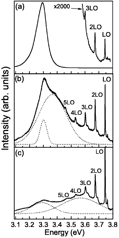
Shown in Fig. 2a is the spectrum of near-band-edge (NBE) emission of the non-doped film. There one can see the intense band of NBE PL with the peak at and halfwidth , which corresponds to emission of excitons bound at donor and acceptor states [19]. From the low-energy side, asymmetry in the PL band shape can be modeled with Gaussian lines with the distance between their peaks close to the phonon energy ( ), which can be indicative of a high efficiency of recombination processes related with excited charge carriers and phonons.
In PL spectra of films doped with concentrations and (Fig. 2b, с), one can observe a considerable decrease (- and -times) in the intensity of NBE PL bands, respectively. In this case, the PL band peak is shifted to the high-energy side by , which can be indicative of a quantum-sized effect or - electron band mixing. As the dimensions of nanocrystalline regions ( , Fig. 1) are considerably higher than the exciton radius in ZnO ( ) [20], the quantum-sized effect can be neglected. When the concentration increases, there appears and increases the PL band in the high-energy spectral range. It can be modeled by wide Gaussian contours peaking at ( ) and ( ) for and samples, respectively (Figs 2b and 2с). The latter are ascribed by us to emission from two separate regions in , namely: regions enriched and depleted with atoms, which in a good accordance with SEM investigations (Fig. 1). It should be noted that the observed high-energy shift of both NBE PL bands by and cannot be explained by increasing of the concentration in alloy, as it is known that in the wurtzite structure [11]. This blue shift can be caused by the - mixing of wave functions inherent to electrons of the conduction band with localized -states of magnetic impurity. This effect is observed in ferromagnetic semiconductors ( ) and ( ) where the high-energy shift of the intrinsic absorption edge increases with magnetization [21].
Also, NBE PL spectra of films show weak additional emission at caused by relaxation of hot charge carriers with a high concentration (- ).
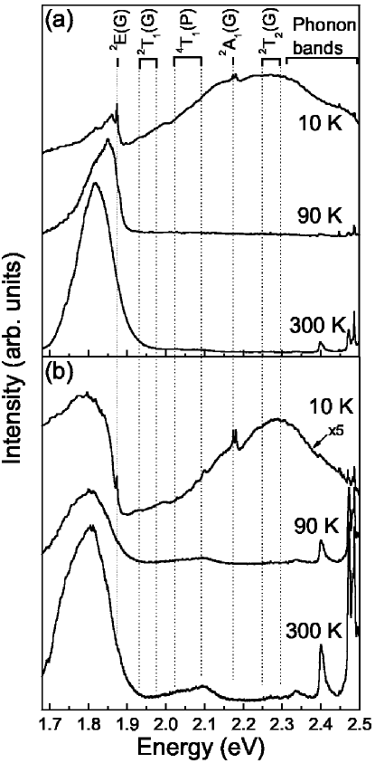
It is worth to note that the intensity of the broad band within the range to related with defects [22], [23],[24], [25] is three orders lower in the non-doped films than that of NBE PL band in films. Depicted in Fig. 3 are the PL spectra of films at various temperatures for the excitation energy lower than the edge of intrinsic absorption in matrix. In films doped with , one can observe the splitting of configurations inherent to ions by electron terms as a result of crystalline field effects in tetragonal surrounding of oxygen atoms. The parameter of crystalline field in is and electron transitions between the ground and excited , , , terms of the ion lie in the forbidden gap of matrix (Fig. 3а) [26].
The narrow emission bands at and eV in low-temperature PL spectra of and samples ( K, Fig. 3) correspond to electron transitions and in the center, respectively. The broad emission bands at , and eV correspond to electron transitions , and , respectively (see the notations of terms for the center in Fig. 3). At the background of the narrow band corresponding to the electron transition in the center, one can observe a broad low-energy emission band that was earlier explained by participation of phonons localized in distorted crystalline field in this electron transition. With increasing the temperature ( K), PL spectra show a considerable decrease in the intensity of emission bands within the range of high-energy electron transitions in the center, and sharp peaks disappear. However, the intensity of the PL band related with the lowest electron transition increases in the temperature range from to K, and the band becomes widen and shifted to the low-energy side by (Fig. 3), which can be explained both by the influence of electro-phonon processes and broadening the ground level of the interacting centers.
As known, the electron terms , and take an active part in charge transfer processes for electrons from/onto the center with creation of and states [11]. Therefore, it seems reasonable to assume that the absence PL bands related with these terms at room temperature can be indicative of availability of nonemission electron transitions from these states to the conduction band of matrix.
Phonon properties of and films were investigated using micro-Raman scattering in geometry, where the axis is directed along the wurtzite -axis. crystals possess the hexagonal wurtzite structure (spatial symmetry group ). In accord with the theory-group analysis, in the -point of the Brillouin zone the phonon modes belong to the irreducible representation: . The modes , and are active in Raman spectra, while the modes of symmetry are the so-called ”silent” modes, i.e., these cannot be observed in Raman spectra. In non-resonant Raman spectra of non-doped films with eV, one can observe the intense and phonon modes at ( ) and ( ), respectively (Figs 4 and 5). The observed high-frequency shift of the mode by as compared with bulk corresponds to bi-axial compression strains in the plane perpendicular to the -axis. The difference two-phonon mode is observed at . The mode at possesses very low intensity in high-quality films, which is related with destructive interference between Fröehlich interaction and deformation potential contribution to the scattering in [27]. The observed phonon modes correspond to wurtzite crystal [28]. The asterisk in Fig. 5 indicates the intense phonon mode of symmetry at , which is inherent to sapphire substrate.
Doping the films with atoms causes structural disordering the crystalline lattice and stoichiometric changes in it. As the non-polar mode corresponds to oscillations of metal atoms, and - to oscillations of oxygen atoms in the plane normal to -axis, they are very sensitive to disordering both in cation and anion sub-lattices, respectively. With increasing the concentration in the studied samples, the intensity of these modes decreases. () mode is shifted to the red (blue) spectral ranges by () and is broadened up to () as a consequence of structural disordering and violation of the translation symmetry in metal (oxygen) sub-lattices and/or creation of solid solution.
Also, new additional broad bands appear within the range - (Figs 4 and 5) [29] in Raman spectra of films. In general, these bands can be caused by -impurity substitution in cation sublattice and correspond both to local resonant impurity oscillations and impurity-activated vibration bands related with forbidden Raman scattering with wave vectors of phonon density of states, in particular, as a consequence of selection rule violation [30]. It is very difficult to distinguish between these two types of vibrations in Raman spectra, as their frequencies are close [30]. It is appropriate to note that that forbidden Raman scattering was also observed in magnetic materials, in particular in halogenides of transition elements (), where the multi-phonon -process of scattering caused by spin disordering and mixing between electron and magnetic excitations is dominant [18]. The broad band at is ascribed to surface optical phonons (SP-mode) that can be detected with the frequency position between and modes in nanostructures with the sizes [31]. It should be noted that in Raman spectra of the studied films, we did not found any additional phonon bands that could correspond to secondary structural phases such as or [15].
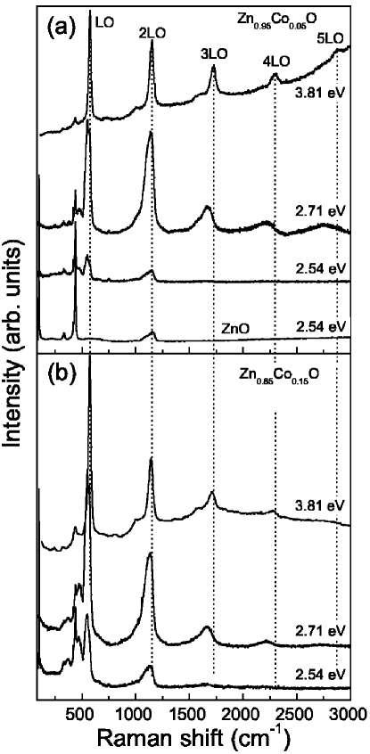
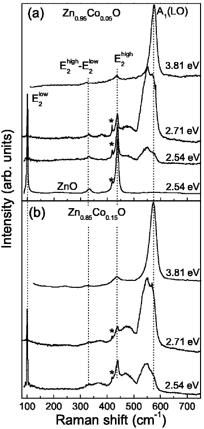
Shown in Fig. 4 are the Raman spectra of films under subband excitation ( and ) as well as under resonant excitation within the range of intrinsic absorption ( ). In these spectra, one can see the bands caused by the multi-phonon -process of resonant Raman scattering that will be analyzed in detail below.
Fig. 5 illustrates well resolved Raman spectra of the first order for films within the frequency range to . It is known that structural defects and local fluctuations of the component composition for alloy cause violation of the selection rules as to the wave vector (), which provides participation of phonons with arbitrary wave vectors in the process of Raman scattering. Thus, the sharp peaks in the intense band at that is observed in various geometries of experiments can be related with the van Hove singularities or with critical points located in directions of high symmetry in the Brillouin zone and correspond to maximum values of the density of single-phonon states in ZnO [32] and/or to the frequency of local Co-impurity resonant vibrations.
In spectra of resonant Raman scattering, when the energy of excitation quantum is close or higher than the energy of real electron states in semiconductor, one can detect bands that correspond to multi-phonon -process of scattering caused by the Fröehlich electron-phonon mechanism of interaction [33]. It means that the resonant Raman scattering may be useful when studying the interband energy electron transitions in semiconductors. The multi-phonon scattering by -phonons was observed in resonant Raman scattering in monocrystalline bulk , films and nanowires. In all these cases, excitation of Raman spectra in samples was performed using the discrete emission line from a - laser with the energy ( ) that is lower than the width of forbidden gap, which corresponds to the condition of input resonance with interband electron transition. As seen from Fig. 4, in the resonant Raman spectra of the studied films, on the broad background of edge luminescent emission, one can observe -phonon modes at , , … for and at , , … for that correspond to , , , and phonon bands of (Figs 4 and 5). Rather extraordinary was the effect that when exciting the Raman spectra in films with the quantum energy within the range to (subband excitation), one can observe a considerable (approximately -times) increase in the intensity of the signal and multi-phonon -scattering up to the fifth order (Fig. 4). It is unambiguous confirmation of the resonant Raman scattering process.
It is noteworthy that this resonant dependence was observed only in -doped samples. Unusual was the observed low-frequency shift of all the -phonon repetitions under subband ( and ) as compared with band-to-band ( ) excitation in micro-Raman spectra obtained from the same local region of the sample. When using the subband excitation, it is rather difficult to estimate the value of frequency shifts with account of the frequency position inherent to band of the first and band of the second scattering order. This cumbersome situation can be caused by the fact that in our micro-Raman experiments we study a local region with the diameter where available are at least two nano-regions of alloys with various component compositions (both enriched and depleted with , Fig. 1). As a result, we have simultaneously observed two resonant processes of Raman scattering with different degree of efficiency in local regions of samples. In the case of dominant resonant process in the film, the frequency shift of line of the third order is close to and for concentrations and . Note that the effect of frequency change for phonons in resonant Raman spectra cannot be explained by only participation of the Brillouin zone with in the multi-phonon process of phonon scattering, which was observed in films () [34]. In the opposite case, the -phonon frequency could be the same under subband and band-to-band excitation.

To explain the resonant character of Raman spectra under subband excitation, we have proposed the following energy diagram for films (Fig. 6). Using the determined from PL spectra (Fig. 3) energy positions of emission bands that correspond to intra-center optical transitions from the ground state to the excited states of electron transitions , and inherent to the ion , we estimated the depth of the ground level for this center relatively to the edge of valence band as to . Due to partially filled shells, the impurity atoms can exist in various charge states. As to , it is adopted that change in the charge state of -impurity is possible either due to shallow donor centers (vacancies of oxygen, , , interstitial zinc , ) or under photoionization by light. It was formed the bounding states due to the long-range Coulomb interaction as a result an electron occupies by the hydrogen-like orbital of the donors. The excited states of -defect centers together with the donor states of host are formed a defect exciton [35]. So, it was observed the resonant Raman processes and a selective enhancement in multi-phonon scattering by phonons. Our results show that the intermediated states in multi-phonon scattering by phonons in under sub-bandgap excitation is a excited state of -defect centers bounded to a the localized exciton with the Fröhlich mechanism. This approach of the resonant enhancement is a similar one observed for () semiconductors in multi-phonon scattering by phonons which is due to a strong interaction phonons with localized electrons in non-filled -shells [18].
Existence of magnetic excitations related to the ground state of center with the frequency in the ferromagnetic phase () provides creation of a magnetic sub-band that consists of the states , , etc [36]. Mixing the magnon-phonon excitations results in the low-frequency shift and broadening the orders of phonons in resonant Raman spectra under sub-band excitations in -doped films. The analysis of low-frequency shifts of -phonon repetitions in the Raman spectra under resonant and non-resonant excitation conditions allows estimating the band width for magnetic sub-system.
4 Conclusion
In this paper, we have studied the optical and electronic properties of the MBE-grown non-doped, and -doped thin films. SEM and AFM investigations have found that with growth of the concentration the grain diameter is decreased, and one can observe spinodal component decomposition of alloys. It results in inhomogeneous distribution of atoms. There arise local regions enriched and depleted with that possess the dimensions within the range .
In the spectra of band-to-band PL, one can detect two bands, which is in accord with the possibility of creation of two regions with different the concentration. The band that corresponds to a higher concentration of atoms is shifted to the high-energy side as compared with the band corresponding to regions with a lower concentration. The shift to the high-energy side is a result of - mixing of wave functions inherent to electrons of the conduction band with localized -states of magnetic impurity.
In temperature-dependent PL spectra under excitation energies lying in the visible range, we have detected energy transitions in the center: , , , , , positions of which did not depend on the concentration in matrix.
Under band-to-band and sub-band excitation, we have detected resonant multi-phonon Raman spectra in films. It has been investigated the dependence of the intensity for -phonon mode on the energy of exciting laser radiation. We have shown the possibility to study excited states of the center in by using the resonant Raman effect. It allows studying the excited states of centers that have no luminescence.
References
References
- [1] Thomas D 1960 J. Phys. Chem. Solids 15 86
- [2] Chambers S 2010 Adv. Materials 22 219
- [3] Schwartz D, Norberg N, Nguyen Q, Parker J, Gamelin D 2003 J. Am. Chem. Soc. 125 13205
- [4] Ueda K, Tabata H and Kawai T 2001 Appl. Phys. Lett. 79 988
- [5] Dietl T, Ohno H, Matsukura F, Cibert J, Ferrand D 2000 Science 287 1019
- [6] Coey J, Venkatesan M, Fitzgerald C 2005 Nat. Mater. 4 173
- [7] Kohan A, Ceder G, Morgan D, Van de Walle C 2000 Phys. Rev. B 61 15019
- [8] Dietl T, Spalek J 1982 Phys. Rev. Lett. 48 355
- [9] Sato K, Katayama-Yoshida H, Dederichs P 2005 Japanese J. of Appl. Phys. 44 L948
- [10] Straumal B, Mazilkin A, Protasova S, Myatiev A, Straumal P, Baretzky B 2008 Acta Materialia 56 6246
- [11] White M, Ochsenbein S, and Gamelin D 2008 Chem. Mater. 20 7107
- [12] Dietl T, Andrearczyk T, Lipinska A, Kiecana M, Tay M, Wu Y 2007 Phys. Rev. B 76 155312
- [13] Kuroda S, Nishizawa N, Takita K, Mitome M, Bando Y, Osuch K, Dietl T 2007 Nature Materials 6 440
- [14] Yokoyama M, Yamaguchi H, Ogawa T, Tanaka M 2005 J. Appl. Phys. 97 10D317
- [15] Samanta K, Bhattacharya P, Katiyar R, Iwamoto W, Pagliuso P and Rettori C 2006 Phys. Rev. B 73 245213
- [16] Hasuike N, Nishio K, Katoh H, Suzuki A, Isshiki T, Kisoda K, Harima H 2009 J. Phys.: Condens. Matter 21 064215
- [17] Friedrich F, Nickel N 2007 Appl. Phys. Lett. 91 111903
- [18] Güntherodt G and Zeyher R 1984 Light Scattering in Solids IV, Springer series in Topics in Applied Physics vol 54, (Berlin: Springer-Verlag) p 517
- [19] Chen Y, Liu Y, Lu S, Xu C, Shao C, Wang C, Zhang J, Lu Y, Shen D, and Fan X, 2005 J. Chem. Phys. 123 134701
- [20] Fonoberov V, Alim K, Balandin A, Xiu F, and Liu J 2006 Phys.Rev. B 73 165317
- [21] Lebedeva N and Kuivalainen P 2002 J. Phys. C 14 4491
- [22] Zeng H, Cai W, Hu J, Duan G, Liu P and Li Y 2006 Appl. Phys. Lett. 88 171910
- [23] Kurbanov S, Panin G, Kim T, and Kang T 2009 J. Lumin. 129 1099
- [24] Gong Y, Andelman T, Neumark G, O’Brien S, and Kuskovsky I 2007 Nanoscale Res. Lett. 2 297
- [25] Zubiaga A, García J, Plazaola F, Tuomisto F, Saarinen K, Zuñiga Pérez J, and Muñoz-Sanjosé V 2006 J. Appl. Phys. 99 053516
- [26] Koidl P 1977 Phys. Rev. B 15 2493
- [27] Callender R, Sussman S, Selders M, and Chang R 1973 Phys. Rev. B 7 3788
- [28] Cuscó R, Alarcón-Lladó E, Ibáñez J, Artús L, Jiménez J, Wang B, and Callahan M 2007 Phys. Rev. B 75 165202
- [29] Šćepanović M, Grujić-Brojc̆in M, Srećković K 2010 J. Raman Spectrosc. 41 914
- [30] Zigone M, Vandevyver M, Talwar D 1981 Phys. Rev. B 24 5763
- [31] Fonoberov F, Balandin A 2004 Phys. Rev. B 70 233205
- [32] Serrano J, Romero A, Manjón F, Lauck R, Cardona M, and Rubio A 2004 Phys. Rev. B 69 094306
- [33] Bergman L, Chen X, Morrison J, Huso J, and Purdy A 2004 J. Appl. Phys. 96 675
- [34] Kaschner A, Hoffmann A, and Thomsen C 2001 Phys. Rev. B 64 165314
- [35] Nielsen K, Bauer S, Lübbe M, Goennenwein S, Opel M, Simon J, Mader W, Gross R 2006 phys. stat. sol. (a) 203 3581
- [36] Güntherodt G, Merlin R, and Grünberg P 1979 Phys. Rev. B 20 2834