Also at ]University of Colorado, Boulder
Measurement and modeling of large area normal-metal/insulator/superconductor refrigerator with improved cooling111Contribution of a U.S. government agency, not subject to copyright.
Abstract
In a normal-metal/insulator/superconductor (NIS) tunnel junction refrigerator, the normal-metal electrons are cooled and the dissipated power heats the superconducting electrode. This paper presents a review of the mechanisms by which heat leaves the superconductor and introduces overlayer quasiparticle traps for more effective heatsinking. A comprehensive thermal model is presented that accounts for the described physics, including the behavior of athermal phonons generated by both quasiparticle recombination and trapped quasiparticles. We compare the model to measurements of a large area () NIS refrigerator with overlayer quasiparticle traps, and demonstrate that the model is in good agreement experiment. The refrigerator IV curve at a bath temperature of 300 mK is consistent with an electron temperature of 82 mK. However, evidence from independent thermometer junctions suggests that the refrigerator junction is creating an athermal electron distribution whose total excitation energy corresponds to a higher temperature than is indicated by the refrigerator IV curve.
pacs:
74.70.Ad 74.50.+r 07.20.Mc 85.30.Mn 85.25.Na
I Introduction
In a normal-metal/insulator/superconductor (NIS) tunnel junction biased near the superconducting gap energy , the single quasiparticle tunneling current transfers heat from normal metal electrons to the superconductor. This transfer enables refrigerators that can cool electrons from 300 mK to 100 mK,Leivo et al. (1996); Pekola et al. (2004) and can cool arbitrary payloads as well. For example, NIS refrigerators have been used to cool a macroscopic germanium thermometerClark et al. (2005) and a superconducting transition edge x-ray detector.Miller et al. (2008) The performance of these refrigerators is limited, in part, by heating of the superconductor due to the dissipated power , and the heat removed from the normal metal. The impact of this heating on NIS refrigerator performance is often characterized by the fraction of the power deposited in the superconductor that returns to the normal metal as an excess load.Ullom (2000)
Previous efforts to model the heating of the superconductor in NIS refrigerators to predict have included quasiparticle diffusion, trapping and recombination. For example, Ullom and Fisher numerically solved a differential equation for the excess quasiparticle density vs position in the superconductor.Ullom (2000) Rajauria et alRajauria et al. (2009) used approximations to solve similar differential equations analytically and introduced a finite quasiparticle trapping rate. In that work, a parameter equivalent to was calculated, and the agreement with experiment was within a factor of 3 to 10.
In this paper, we expand upon previous work by providing the most comprehensive model of NIS refrigeration to date. We add a new form of quasiparticle traps, referred to as overlayer traps, to both the model and devices. We model not only the superconductor quasiparticle temperature, but also the overlayer trap electron temperature and the temperature of the phonons in the metal layers that make up the NIS refrigerator. We also account for the athermal behavior of excitations with energy created by quasiparticle relaxation. Our implementation of this model easily handles changes in nearly every input parameter, allowing us to examine a large area of parameter space and design the next generation of NIS refrigerators. We present measurements on a large area NIS refrigerator that agree with the model predictions over a large temperature range. The refrigerator IV curves are consistent with cooling from 300 mK to 82 mK. As discussed in Sec VI the refrigerator may be creating an athermal electron distribution so the interpretation of the cooling results is not straightforward.

II Model Overview
We model a single NIS junction, which makes up half of an SINIS refrigerator, as shown in Fig 1. The important systems in the device are the cooled normal metal electrons , the superconductor quasiparticles , the overlayer electrons , and the combined metal layer phonons . Roughly speaking, the power flow is as follows: a power is deposited in the layer by the NIS refrigerator junction, which increases the quasiparticle density locally above the junction. These quasiparticles may diffuse and recombine, but the majority are trapped into the layer. At this point, they become electronic excitations with energy . Various processes allow these electrons to relax, and the majority of the energy couples via electron-phonon coupling to the system. Because all three metal layers are made of Al, or AlMn, with only thin oxide layers between them, we assume that there is one phonon system shared by all three metal layers. Finally, the phonons in the metal layers relax by coupling to the substrate phonons. Systems in the model are connected by both thermal and athermal processes. The model is summarized as a block diagram in Fig 2.
Section III discusses NIS tunneling, Section IV describes quasiparticle trapping, and a detailed discussion of the rest of the physics underlying the model is found in Appendices A–C. Table 1 shows all the model parameters and typical values. Section V compares the model predictions to measurements on an NIS refrigerator device.
The model consists of four coupled equations, three of which are position dependent. Equation 1 describes the overlayer trap electron temperature . The terms on the right hand side from left to right are due to trapping from , coupling to , and recombination phonons. Equation 2 describes the excess quasiparticle density in the superconductor . The terms from left to right are injection by the junction, trapping to , recombination, and trapping to the side-traps. Equation 3 describes the temperature of the phonons in the combined metal layers . The terms from left to right are coupling to , coupling to layer, and coupling to the substrate. Equation 4 is a power balance equation for the electron temperature of the layer. The terms from left to right are due to the tunnel junction ( is negative during refrigeration), Joule heating, coupling to , two-particle tunneling (Andreev reflections), recombination phonons, phonons generated by trapped quasiparticles, and either stray power or power from a payload.
| (1) | ||||
| (2) | ||||
| (3) | ||||
| (4) |
The variables , , , and are the thicknesses of the , , , and layers, is the electronic thermal conductivity of the layer (Eq 22), the variables describe the relaxation branching ratios of trapped quasiparticles (Eq 17), the variables describe the probability of absorption of athermal phonons of energy in layer (Sec C.4), is the recombination rate of excess quasiparticles (Eq 35), is the thermal quasiparticle density due to the bath temperature, is the quasiparticle diffusion constant (Eq 32), and are functions describing the location of the refrigerator junction and side-traps, is the metal layer phonon thermal conductivity (Eq 37), is the quasiparticle trapping rate (Eq 15), and are electron phonon coupling terms (Eq 23), is the power deposited in the superconductor by the NIS junction (Eq 13), and is power flow across the acoustic mismatch between the Al layers and the substrate (Eq 36). Script terms have units power per unit area or volume, where non-script terms have units of power. All equations are solved numerically, and Eqs 1–3 have boundary conditions at both and .O’Neil (2011)
In the power balance equation (Eq 4) power is deposited in the layer by the NIS junction ( is negative during refrigeration). The temperature reduction is limited by an electron-phonon coupling power , Joule heating , two-particle tunneling dissipation , incident phonon power from quasiparticle recombination , and incident phonon power from trapped quasiparticles . Here, is the resistance of the current path through the layer, is the total tunneling current, is the junction bias voltage, and is the two particle tunneling current (Eq 9).Rajauria et al. (2008) An additional power may be present, such as stray RF power or power dissipated by a cooled payload. A term is often included in Eq 4 and used as an empirical parameter that accounts for heating of the superconductor. For the purposes of this paper we use and account for heating of the superconductor explicitly. One goal of the comprehensive thermal model is to predict from measurable NIS design and material parameters. When we compare model and experimental results in Section V, we use as a comparison metric.
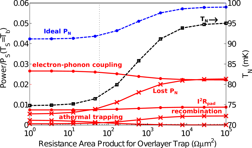
Figure 3 shows the temperatures of the , and layers as calculated by the model for parameters in Table 1. Figure 4 shows the terms in the normal metal power balance (Eq 4) calculated by the model for different values of the overlayer trap barrier resistance area product .

III Superconductors and tunneling
III.1 Quasiparticle density and density of states
This section will briefly review a subset of properties of superconductors which are vital for understanding their behavior in NIS refrigerators. In a superconductor at zero temperature, all the conduction electrons form Cooper pairs which can carry electrical current with zero resistance. At finite temperature, some of the Cooper pairs are broken and each broken Cooper pair yields two quasiparticles. The effective density of states of quasiparticles is given by , where
| (5) |
is the two-spin density of states at the Fermi energy in the same material in the normal state, is the energy relative to the Fermi energy, is the BCS energy gap, and is a unitless factor that describe deviations from the ideal BCS superconducting density of states. The parameter introduces states below the gap energy and is used to account for observed sub-gap tunneling currents greater those predicted with the ideal BCS density of states (). Pekola et alPekola et al. (2010) suggest environment-assisted tunneling as the mechanism responsible for finite .
The quasiparticle density in a superconductor at temperature is
| (6) |
where is the Fermi function at temperature , and is Boltzmann’s constant. To account for equilibrium behavior, we write the total quasiparticle density as the sum of the thermal density at the cryostat bath temperature and the excess density . Relevant quasiparticle distributions are strongly peaked at energy , thus for the purpose of tracking energy during quasiparticle relaxation we treat all quasiparticles as having energy . When we describe the superconductor as having a temperature , we choose to have the correct quasiparticle density.
III.2 NIS Tunneling
The current in an NIS junction is made up of two parts
| (7) | ||||
| (8) | ||||
| (9) | ||||
| (10) |
where is the single particle tunneling current, is the two particle tunneling current, is the two particle contribution from the normal metal electrode in the simplest geometry of an infinite uniform junction,Hekking and Nazarov (1994) is the two particle contribution from the superconducting electrode, is the electron charge, is the tunneling resistance, is the product of the tunneling resistance and junction area, and is the voltage difference across the junction.
The form and magnitude of the two particle tunneling current depends on electron interference due to multiple scatterings, and therefore, on the geometry of the electrodes. We rely on theoretical forms of and from Hekking and NazarovHekking and Nazarov (1994) which are not specific to our junction geometries. The form of in Eqs 9 and 10 is in rough agreement with our data, and we have an ongoing investigation to improve our understanding of the precise form of for our geometry.Lowell et al. (2011) We have excluded the contribution from the superconducting electrode in this work because 1) due to the thickness of the superconductor 2) the overlayer traps should further suppress multiple reflections and thus the magnitude of and 3) the theory of in Hekking and NazarovHekking and Nazarov (1994) breaks down for biases , which are commonly used for cooling. In most cases , however at low temperatures and low biases . For the junctions described in this work plays a small role; is more important for junctions with lower resistance area products.
The complete current-voltage (IV) relationship also includes a resistive voltage due to the normal metal electrode
| (11) |
The power deposited in the normal metal by single particle tunneling is
| (12) | ||||
Refrigeration is possible because is negative for biases such that . Note that is a function of both and (through and ), and this dependence on is the reason that superconductor heating directly impacts NIS performance. The two particle tunneling current deposits power and Joule heating deposits power in the normal metal.Rajauria et al. (2008)
The power deposited in the superconductor is
| (13) |
Both the quasiparticle thermal population, and the quasiparticles injected into the layer by the NIS junction are strongly peaked at . We approximate the quasiparticle injection rate as , which is justified because and in the regime of interest for NIS refrigerators. The power deposited in the superconductor per unit area is calculated by substituting the resistance area product of the tunnel junction in place of the resistance .
IV Quasiparticle trapping
IV.1 NIS junction as a quasiparticle trap
Power will flow across an NIS junction even when , if the normal metal temperature and superconductor temperature are unequal. In NIS refrigerator operation, the layer is directly heated and therefore is hotter than the layer. As a result, power will flow from the to the layer, providing an additional mechanism for the superconductor to reach thermal equilibrium. The unbiased NIS junction between the and layers, combined with the layer form a quasiparticle trap used to heatsink the superconductor. The power flow per unit area from the superconductor is given by
| (14) | ||||
| (15) |
where we have used the approximation that all quasiparticles have energy to obtain Eq 15.
The tunneling lifetime of an electron in a thin metal film adjacent to a tunnel barrier is
| (16) |
where is the film thickness and is the resistance area product of the tunneling barrier. The tunneling lifetime grows with film thickness and also with the resistance area product of the tunnel junction. The lifetime for quasiparticles to trap from the to the , or to tunnel back from the to the layer is ns, based upon thickness nm, and a tunnel barrier with resistance area product .
IV.2 What happens to a trapped quasiparticle?
A quasiparticle which tunnels from the into the layer becomes an excited electron with energy . There are three processes available to this electron: 1) tunneling back into the superconductor with lifetime ns, 2) scattering with another electron with lifetime ns, and 3) scatter and create a phonon with lifetime ns. Once the excited electron has scattered with either a phonon or an electron, it will have energy less than and be unable to tunnel back into the superconductor, thus the name quasiparticle trap.Booth (1987) However, the most likely phonon to be created will have energy which is well above the thermal distribution.Ullom (1999) A phonon has a finite probability of being absorbed in the layer, and if this happens regularly it will severely degrade the benefit of quasiparticle traps. Appendices A.1–A.4 describe these mechanisms and the methods used to calculate the time constants.
We estimate the probability of scattering to create a phonon , to tunnel back to the superconductor , or to undergo electron-electron scattering as
| (17) |
For eV, of the quasiparticles removed from the layer will generate athermal phonons, tunnel back to the superconductor, and only are thermalized by electron-electron scattering. The most likely energy for these athermal phonons is , so of the energy which tunnels from to becomes athermal phonons. Appendix C.4 describes a ray tracing model which predicts the fraction of these athermal phonons that deposit their energy in the other layers. The majority of athermal phonons will be reabsorbed before leaving the layer, making the overlayer traps more effective than these probabilities suggest on their own.
V Experimental Methods and Results
SINIS refrigerator devices were fabricated on a Si wafer with 150 nm of thermally grown SiO2. The layer is 20 nm of sputter deposited Al with ppma222Parts per million by atomic percent (ppma) is used in this work, however parts per million by weight (ppmw) is commonly used by commercial vendors and analysis labs. Mn. The layer and all subsequent layers are patterned with standard photolithography techniques. The metal layers are etched with an acid etch. A layer of SiO2 is deposited by plasma enhanced chemical vapor deposition and etched with a plasma etch. The vias etched in the SiO2 define the location of the tunnel junctions. The wafer is returned to the deposition system where it is ion milled to remove the native oxide from the AlMn, then exposed to a linearly increasing pressure of 99.999 pure O2 gas for 510 seconds, reaching a maximum pressure of 6.0 Torr (800 Pa) to form the tunnel barrier oxide. Then, 500 nm of Al is deposited by sputter deposition to form the layer. The overlayer trap tunnel barrier is formed by exposure to 32 mTorr O2 (4.3 Pa) for 30 s, and 500 nm of AlMn is deposited to form the layer.
One of these devices (inset in Fig 5) was cooled in a copper box attached to the cold stage of an adiabatic demagnetization refrigerator. We measured current-voltage () curves of the SINIS device (and the independent thermometer junctions) at many bath temperatures . The bias of the refrigerators (independent thermometers) was set with a computer-controlled, battery-powered voltage source connected through a 100 k (10 M) bias resistor. The voltage across the device was amplified with an operational amplifier and the output of the amplifier was measured by a digital multimeter. The current was calculated as the source voltage minus the device voltage divided by the bias resistance.
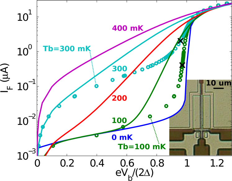
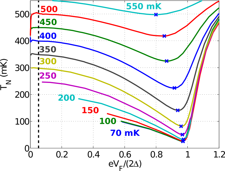
The primary experimental results we report come from thermometry based on the refrigerator junctions. Each data point ( and ) is an independent measurement of the normal metal temperature , which depends on both bath temperature and refrigerator bias . The temperature at each point is uniquely determined by comparison to isothermal theory curves (Eqs 7 and 11), as shown in Fig 5. Temperatures determined from NIS junctions in this way are effective temperatures because Fermi occupation functions are assumed in the junction electrodes. For a thermal electron distribution this effective temperature will match the actual temperature. For athermal electron distributions, the NIS effective temperature does not provide a complete description. Figure 6 shows effective temperature vs refrigerator bias for many bath temperatures.
For each bath temperature, we determine the bias point at which the minimum value of is reached. We call this the optimal bias. The value of at the optimal bias is shown vs bath temperature in Fig 7. Figure 7 also shows the value of at a bias voltage of 20 . For bath temperatures above mK the temperature determined at a bias voltage of 20 should equal the bath temperature because the NIS junctions have little thermal effect at low biases. We determine by a least squares minimization between the temperature deduced from IV curves at low bias (20 ) and the temperature measured by the cryostat thermometer. The layer resistance is calculated as in Table 1, the tunneling resistance is the asymptotic resistance at high bias and high temperature minus , and is chosen to match the maximum differential resistance at 70 mK.
The data from the refrigerator IVs indicate significantly improved cooling compared to previous large area (m2) NIS refrigerators.Clark et al. (2004) Assuming a thermal electron distribution in the normal metal, we deduce cooling from 300 mK to 82 mK and from 100 mK to 26 mK.
VI Independent thermometers and athermal electron distributions
Current-voltage curves from the independent thermometers can be used to obtain temperature values using a procedure similar to that described in the previous section. As shown in Fig 7, the thermometer data suggests hotter electron temperatures than those deduced from the refrigerators. The thermometer junctions were fabricated using a double oxidation technique and their resistance area product was 145,000 m2, over 100 times greater than the refrigerators.Holmqvist et al. (2008); O’Neil (2011) This high resistance makes the thermometers thermally neutral, meaning they neither heat nor cool the normal metal. We next consider thermal mechanisms for a temperature gradient between the thermometers and refrigerators.
We expect a small temperature difference between the refrigerator and thermometer junctions due to the finite thermal conductivity of the normal electrode and the presence of power loads within it. We calculate the expected difference by solving the heat equation in the N layer including electron-phonon coupling and stray power:
| (18) |
We let x vary from 0 to 10 microns with corresponding to the edge of the refrigerator junction, corresponding to the end of the AlMn, and to corresponding to the thermometer junction. We fix at at and vary the refrigerator temperature at until the thermometer temperature (evaluated at ) matches the measured temperature. The variable is the thermal conductivity of the normal layer and is obtained from Eq 22. The stray power pW is obtained from thermometer junction temperature measurements with the refrigerator junctions at zero bias. Finally, is the N layer volume. The observed thermometer temperatures and the refrigerator temperatures calculated from these thermometer temperatures are shown in Fig 7. The gradient varies from 0.02 mK to 7 mK for bath temperatures between 100 mK and 500 mK. This gradient accounts for over half of the observed difference at a bath temperature of 500 mK but does not explain the observed difference near 100 mK. We hypothesize that the remaining differences in temperature result from an athermal electron distribution created by the refrigerators that recovers to a thermal distribution over the distance to the thermometers.
NIS refrigerators generate an athermal electron distribution when the tunneling rate is faster than inelastic scattering in the normal electrode. The tunneling time for electrons above the gap edge is insensitive to temperature, and the rates for inelastic electron-electron and electron-phonon scattering both decrease with temperature. As a result, athermal effects in NIS junctions appear near or below mK.Pekola et al. (2004) The athermal electron distribution created by the refrigerators lacks the high energy excitations ordinarily found in the tips of a Fermi distribution. However, its total excitation energy will exceed that of the thermal distribution that results in the same tunneling current.
Over the distance between the refrigerator and thermometer junctions, the athermal distribution recovers to a thermal one through inelastic scattering and the tips of the Fermi distribution are repopulated. Consequently, additional current flows through the thermometers and a higher device temperature is deduced even though the thermal electron distribution at the thermometers and the athermal distribution at the refrigerators contain the same excitation energy (neglecting the small gradients calculated above). We observe that the temperature deduced from the thermometers is largely independent of their bias point, supporting the notion of a thermal electron distribution at the thermometer junctions. Further, athermal electron distributions in metals with similar diffusion constants to our normal layer have been observed to thermalize over distances as short as 2.5 m.Pothier et al. (1997)
Our results illustrate the complexities of junction thermometry. Experiments that use the same junctions as both refrigerators and thermometers are susceptible to athermal effects. Similarly, if independent thermometer junctions are close enough to the refrigerators that they sample the same athermal distribution, the inferred temperature reduction may be exaggerated. We have provided temperature values deduced from both refrigerator and distant thermometer junctions. While the thermometers likely provide a truer measurement of temperature, the results from the refrigerators still have value as a measure of the distortion of the electron distribution in our devices.
We note that our equilibrium thermal model predicts temperatures close to the values deduced from the refrigerator IVs, rather than the independent thermometers. This outcome is not surprising. While the model finds the temperature where the power loads balance, it can also be thought of as finding the junction current at thermal balance. In the presence of an athermal electronic distribution, current remains a good predictor of key power loads such as the Joule term and the heating of the superconductor. Hence, the model correctly predicts refrigerator currents together with the temperature that produces these currents assuming a thermal distribution. Since the refrigerator temperatures are deduced from measured currents assuming a thermal distribution, model and refrigerator measurements give similar temperature values.
VII Analysis and comparison to model
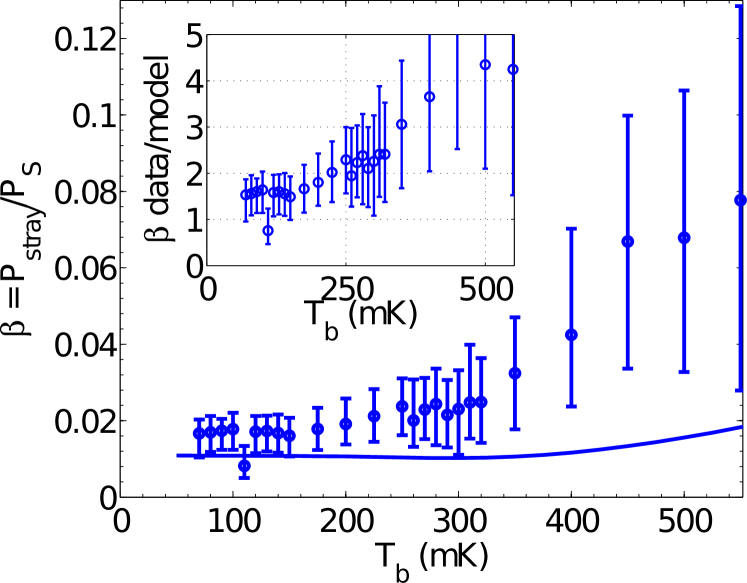
Since knowledge of the precise details of the electron distribution under refrigeration is lacking, for the purposes of this section we henceforth assume a Fermi distribution in the normal metal and continue our analysis of the results from that perspective. We calculate vs bath temperature and compare to predictions of the thermal model, results are shown in Fig 8. In order to determine the value of in the device, we calculate the excess power load required to explain the measured value of at the optimal bias at each bath temperature;
| (19) |
where is the tunneling resistance of the two refrigerator junctions in series, the factors of 2 account for the existence of two junctions, is given in Eq 12, and are the optimal bias voltage and current for a given bath temperature, is the layer electron temperature at the optimal bias, is the resistance of the layer current path, is the layer volume, and is the electron phonon coupling constant. The value of is calculated by
| (20) |
where is the dissipated power, and the denominator is the total power deposited in the layer. The measured value of is therefore a complicated combination of measurement and analysis that depends on the parameters , , , , and , and the accuracy of the underlying theory. We generate error bars on using estimates of the uncertainty of each parameter propagated through the calculation. The uncertainties used to generate the error bars are and . The sum of and was held constant. Variation in affects the determination of and directly enters the calculations of . At higher temperatures uncertainty in determines the bulk of the error bars; at lower temperatures uncertainty in dominates. The range of 300 mK and below is the most interesting range for Al-based NIS refrigerators. In this range, the measured value of is roughly 1.5 times the predicted value, which is better agreement than past NIS modeling has achieved. For higher temperatures, the agreement is not as good, suggesting that improvement could be made by focusing on features of the model whose relative importance increases with temperature, such as quasiparticle recombination and electron-phonon coupling. Underwood et alUnderwood et al. (2011) observe that the exponent in the electron phonon coupling depends on temperature for temperatures above mK; including this effect may improve agreement at higher temperatures.

VIII Future Refrigerator designs based on thermal model
By exploring the design parameter space with the thermal model, we have developed an NIS design that is predicted to cool from 100 mK to 6.5 mK. The overlayer trap resistance is decreased to 1 , the overlayer thickness is increased to 10 , the Dynes parameter is reduced to the lowest reported valuePekola et al. (2010) of 38000-1, and the junction length parallel to current flow is reduced to 3 .
The same changes that we suggest to improve cooling from 100 mK will also improve cooling from higher temperatures with lower resistance area product refrigerator junctions. A device with the changes above, increased layer thickness of nm, and decreased the resistance area product of =150 is predicted to cool from 300 mK to 48 mK. If the overlayer thickness is left unchanged at 500 nm, the device should cool to 64 mK. Junctions with this low resistance area product are difficult to fabricate with high yield, so it is not a simple step to achieve these performance levels. These predictions demonstrate the capability of the model to explore a large design space. Refrigerators based on these designs will generate electron distributions that vary further from the Fermi distribution than the refrigerator discussed here.
IX Conclusions
We have described a comprehensive NIS refrigerator thermal model that includes differential equations for three temperatures vs position, and accounts for the athermal behavior of high energy excitations. The predictions of this zero free parameter model agree well with experimental results from an NIS refrigerator with overlayer traps. The agreement for the quasiparticle return parameter are within a factor of 1.5 over the temperature range of primary interest. This refrigerator cools more than previous large area (m2) NIS refrigerators. From a bath temperature of 300 mK, the refrigerator junction current is consistent with cooling to 82 mK. However, the refrigerators likely generate an athermal electron distribution, and as a result the cooling cannot be described simply. Thermometer junctions which probe the temperature m away from the athermal distribution measure a temperature 114 mK.
This work expands upon previous modeling efforts by including more coupled temperatures systems (the overlayer electrons and the metal layer phonons) and more athermal effects. The model could be further improved by including more detail in the form of the electron-phonon coupling, and by calculating the electron distribution in the normal metal electrode. We plan to perform phonon cooling experiments that will provide a direct measurement of the usable temperature reduction from similar refrigerator junctions.
Acknowledgements.
We benefited from the help of many other members of the Quantum Sensors Program and Quantum Fabrication Facility. This work was funded by the NASA APRA Program and the NRC RAP.Appendix A Electron excitation behavior in a normal metal
To calculate the temperature of the layer, the layer, and the effect of athermal excitations in both layers, we must understand the heat transport and loss mechanisms in both a superconductor and a normal metal. In particular, we want to understand what happens when a quasiparticle is trapped in the layer.
A.1 Electron diffusion in the normal metal
The numerous elastic collisions off impurities, grain boundaries, and surfaces cause electrons to diffuse, rather than move ballistically, through a normal metal. The diffusion constant for electrons in a normal metal isKittel (1996)
| (21) |
where is the elastic mean free path and m/s is the Fermi velocity for Al. From this we calculate the elastic mean free paths in the layers of the NIS refrigerator to be nm, nm and nm.
A.2 Thermal transport in normal metal electrons
The Wiedemann-Franz law relates the thermal conductivity of the electron system to the resistivity by
| (22) |
where W /K2 is the Lorenz number.Kittel (1996)
A.3 Electron-phonon interaction in normal metals
Electron and phonon populations occupying the same volume of a normal metal interact via the electric field from phonons displacing lattice ions.Reizer (1989); Ullom (1999) This interaction leads to a power per unit volume flowing from the phonon system to the electron system of the form
| (23) |
where is the phonon temperature, is the electron temperature, is the electron-phonon coupling constant, and is an exponent whose value can vary from 4 to 6 depending on the properties of the metal film. Previous work on NIS junctions with AlMn base electrodes has used .Clark et al. (2005) However, recent measurements by UnderwoodUnderwood et al. (2011) and TaskinenTaskinen and Maasilta (2006) show that is more accurate for AlMn films in the temperature range of interest.
A.3.1 Electron-phonon interaction: Electron scattering time
UllomUllom (1999) extended theoretical calculations for to find , the characteristic time for an electron to down scatter with the creation a phonon. In the case where =5 in Eq 23
| (24) |
where =.
To obtain for the case we use an energy scaling argument to modify Eq 24. A method to estimate the electron lifetime for phonon scattering is where is the electron heat capacityKittel (1996) per unit volume and
| (25) |
is the electron-phonon thermal conductivity. Thus . This method underestimates because it represents an average of over thermal occupation, and the energy dependence of is strong. However, this method accurately predicts the energy scaling of . Therefore we modify Eq 24 for by replacing with . The result is
| (26) |
We introduce the notation ns, to represent evaluated at energy .
An electron scattering with emission of a phononUllom (1999) with initial energy will have average final energy with the emission of a phonon of energy .333See supplemental material. Since this phonon’s energy is well above the thermal distribution at 300 mK its athermal behavior must be accounted for, as described in Appendix C.4.
A.3.2 Electron-phonon interaction: Phonon scattering time
The energy dependence of the lifetime for a phonon of energy to lose energy by scattering and promoting an electron is weaker than for , so the approximation is more appropriate. Using the Debye result for phonon heat capacity,
| (27) |
A.4 Electron-electron scattering
The electron-electron scattering rate is strongly dependent on the effective dimensionality of the sample, and the degree of disorder present. Therefore, we will first look at the criteria for the 2D/3D limits and the clean/dirty limits.
A.4.1 2D vs 3D scattering
The material is in the 2D limit if the excitation energy of the electron is less than the uncertainty in the energy associated with the transit time across the thinnest dimension, that is . Otherwise it is in the 3D limit. All of the films here are thicker than the elastic mean free path so the transit time is where is the diffusion constant. Therefore s and s. The excitation energy of most interest for scattering is , and s.Ullom (1999) We determine that the layer is in the 3D limit and the layer is in the 2D limit for electrons with energy , such as trapped quasiparticles.
A.4.2 Electron-electron scattering: clean vs dirty scattering
The relevant condition for clean vs dirty electron-electron scattering limits is different in the 2D and 3D cases. In 3D, dirty scattering dominates when and in 2D dirty scattering dominates when . The layer is in the dirty limit, and the layer is in the clean limit.
A.4.3 Electron-electron scattering time:
The layer films look 3D and clean to electrons of energy , and the layer films look 2D and dirty to the same electrons. Therefore the electron-electron scattering times are given by
| (28) | ||||
| (29) |
where K. When an electron with initial energy scatters, the average final energy is with the creation of two new excitations, an electron and a hole, each with energy .Ullom (1999); Al’tshuler and Aranov (1979); Santhanam and Prober (1984)
Appendix B Excitation behavior in a superconductor
Having looked at the mechanisms of thermalization that take place in a normal metal, we now examine their analogs in a superconductor. Quasiparticles undergo diffusion by many elastic collisions, much like electrons, but inelastic scattering is rare for quasiparticles with energy . Instead, the most common method for quasiparticle relaxation is recombination, whereby two quasiparticles combine to form one Cooper pair and one athermal phonon with energy .
B.1 Quasiparticle diffusion
We treat all quasiparticles as having equal energy with one exception. This exception is the quasiparticle group velocity, which is strongly energy dependent and approaches zero as approaches . The group velocity for a quasiparticle excitation of energy isUllom (1999); Ullom et al. (1998); Bardeen et al. (1959)
| (30) | ||||
| (31) |
The diffusion constant for quasiparticles in a superconductor is modified compared to the normal state by this group velocity, such that . However, the quasiparticle distribution most relevant to NIS refrigeration is not thermal.
An NIS refrigerator junction injects an athermal distribution of quasiparticles into the layer. The diffusion constant for these injected quasiparticles is
| (32) |
where is the quasiparticle injection rate, which can be calculated with this same integral with . For an NIS refrigerator cooling from 300 mK to 100 mK, and are typical values.
B.2 Quasiparticle-phonon scattering
Like an excited electron in a normal metal, a quasiparticle can relax to a lower energy state by emitting a phonon. The lifetime for this is . High energy quasiparticles relax at a rate almost identical to high energy electrons in a normal metal. For energies close to , quasiparticle-phonon scattering is rare. In Al at a temperature of 250 mK and an excitation energy of , the scattering time is many microseconds. Therefore, will be much longer than other relevant time constants and quasiparticle-phonon scattering is not considered for the NIS refrigerators discussed hereUllom (1999).
B.3 Quasiparticle-quasiparticle recombination
Two quasiparticles can recombine to form a Cooper pair and emit a phonon with energy equal to the sum of their excitation energies. This will result in athermal phonons with energy , whose behavior is described in Appendix C.4. Since recombination is a two-body process, the recombination rate scales as the number of pairing possibilities
| (33) |
where is the quasiparticle density. The coefficient depends on material properties,
| (34) |
where is a material specific parameter, whose value we take to be ns in the layer.Chi and Clarke (1979) In order to compare the recombination rate to other time constants, it is useful to define . For thermal quasiparticle populations at 300 mK and 400 mK, s and 1.0 s respectively. Recent measurements of quasiparticle lifetime in Al by Barends et alBarends et al. (2009) provide a check to these calculations. At 210 mK, they measure a lifetime of about 180 s and we calculate s, which is in very good agreement.
In the thermal model, we separate the total quasiparticle density into two parts, the thermal density evaluated at temperature and the excess density . The excess density is an effective increase in the superconductor quasiparticle system temperature due to the power deposited by an NIS junction. The rate of excess quasiparticle recombination is given by
| (35) |

B.4 Phonon-quasiparticle scattering or “pair breaking”
The excitation of electrons by phonons has already been discussed in a normal metal. A similar process can occur in a superconductor where a phonon of energy or greater destroys a Cooper pair and produces two quasiparticles. When two quasiparticles recombine, the emitted phonon has sufficient energy to break another Cooper pair. The pair breaking time for a phonon is given by KaplanKaplan et al. (1976) and is equal to a material specific parameter ps for Al. This number is only weakly dependent on temperature and phonon energy. For example, the rate is only faster for a phonon compared to a phonon.
Appendix C Phonon escape
Ideally, phonons generated by quasiparticle recombination or electron-phonon scattering escape into the Si substrate, but may instead interact with electrons or quasiparticles before leaving the Al and AlMn layers that make up the NIS refrigerator.
While the electrons in the , , and layers are isolated from each other by tunnel barriers, the phonons are not similarly isolated. All three layers are Al with only small quantities ( ppma) of Mn in the and layers, so phonons should freely pass between these layers. However, the metal layers making up the NIS refrigerator are deposited on nm of SiO2 on a Si wafer 300 m thick, and because of this material mismatch the phonons will not always escape into the Si wafer. The Si wafer is treated as an ideal thermal bath at temperature . We model the behavior of thermal phonons using an acoustic mismatch boundary resistance, and the athermal phonons using a ray tracing model.
C.1 Thermal phonons: acoustic mismatch
Phonon thermal resistance at the interface between two different materials arises from reflection due to differences in the speed of sound and is known as acoustic mismatch. The power flow per unit area from phonons in the combined metal layers at temperature to a SiO2 layer at temperature is
| (36) |
where pW/( K4) for Al on SiO2.Swartz and Pohl (1987)
C.2 Thermal phonons: thermal conductivity
The thermal conductivity of the phonons in the combined metals layers can be calculated as where is the Debye model heat capacity for phonons, is the mean free path, and is the average phonon speed. Boundary scattering limits the phonon mean free path at low temperatures, so we approximate . Therefore
| (37) |
where the average speed of sound m/s is a weighted average of the longitudinal m/s and transverse m/s values for Al. One could use a different value of for phonons originating in the superconductor (primarily longitudinal) or the normal metal (primarily transverse),Reizer (1989); Underwood et al. (2011) but the choice of weighting for has only a small impact on the results of the thermal model. The extreme cases of and result in values of that differ by mK, for the parameters in Table 1.
C.3 Phonon-phonon scattering
Phonons can relax by splitting into two phonons of lower energy, but this anharmonic decay process is much slower than other relaxation pathways. MarisMaris (1990) states that the lifetime for anharmonic phonon decay is of order , which is 10 ms for phonons of energy in Al. There is experimental evidence for phonon mean free paths of order 1 mm in superconducting materials, consistent with long lifetime for anharmonic decay.Hauser et al. (1999)
C.4 Athermal phonons
Both quasiparticle recombination and electron-phonon scattering by trapped quasiparticles will create athermal phonons. These phonons will interact with electrons or escape before relaxing via anharmonic decay, and therefore their behavior will not be well described by equilibrium physics. In this section, we describe a ray tracing model shown in Fig 9 for calculating the behavior of these phonons.444A ray tracing model is not ideal because the phonon wavelengths are of similar size to the metal thin films. This model is used due to its simplicity and because it results in phonon escape times that scale inversely with the total film thickness, which is consistent with cited work. With this model, we calculate the fraction of these phonons which are absorbed in each metal layer, and the fraction which escape to the bath. The fraction of energy deposited in the layer is of particular interest because of its direct impact on NIS refrigerator performance.
Consider a phonon with energy created at the top of the layer traveling directly downward with speed of sound . The time to propagate from the top of the layer to the interface is . The probability that the phonon scatters with an electron in the layer in this time is . If the phonon enters the layer, the probability that it leaves without interacting is 1 since its energy is below . The probability that it interacts in the layer before reaching the -Bath interface is . The probability that a phonon incident on the -Bath interface escapes to the bath is . Therefore, the probability that a phonon created at the top of the layer escapes to the bath on its first attempt is . The phonon escape probability is averaged over longitudinal and transverse phonons, and angle.Ullom (1999) The value of the escape probability has a very weak effect on the results of the thermal model because most phonons are re-absorbed before they have even a single escape attempt.
A phonon is created in either the layer as shown, or in the layer at position and with direction given by angle relative to the junction. We assume specular reflections. The phonon is given an initial amplitude of 1, which is reduced by a factor in order to propagate the phonon to the next interface, where is the distance to the interface and is the time constant for the phonon to interact in the current layer. When the phonon reaches the interface between the layer and the bath, the amplitude is reduced by a factor where is the transmission probability for a phonon incident on an Al-SiO2 interface. The probability of a phonon being absorbed in each layer or escaping to the bath is then calculated as the sum of all the amplitude reductions which occur in that layer, averaging over all possible initial values for and .
The typical time for an electron of energy to scatter with a phonon is ns. The average distance an electron will diffuse in this time is , which is much greater than the overlayer trap thickness of 0.5 . Therefore all values of are equally likely, although it would be necessary to restrict for thicker layers or greater because falls as increases. All values of are also equally likely.
The variables that result from this calculation are called where is replaced with the energy of the phonon and is replaced with the layer it is associated with. For example is the probability that a phonon from recombination is absorbed in the layer, while is the probability that a phonon from quasiparticle trapping is reabsorbed in the layer.
| Input Parameters | ||
| Parameter | Input Value | Description |
| 1200 | junction resistance area product | |
| 224 | area of a single refrigerator junction | |
| 7 | length of junction parallel to current flow | |
| 1 | fabrication tolerance, contributes excess volume | |
| 0.0663 | resistivity of layer measured at 4 K | |
| 17.5 nm | thickness pf layer | |
| 3 | distance from junction to side-trap | |
| 67.5 | parameter to account for excess layer area | |
| 2.3 nW/( K6) | electron-phonon coupling strength | |
| 60 | resistance area product of the overlayer traps | |
| 0.0443 | resistivity of the layer measured at 4 K | |
| 500 nm | thickness of the layer | |
| 1000 | length of overlayer trap | |
| eV | energy gap in Al | |
| 100 ns | time constant related to quasiparticle recombination rate | |
| 6000 | Dynes parameter, adds finite sub-gap states | |
| 0.00117 | resistivity of the layer in the normal state, measured at 4 K | |
| 500 nm | thickness of the layer | |
| 300 mK | bath temperature provided by the cryostat | |
| 360 pW/( K4) | acoustic mismatch coefficient | |
| 0.71 | athermal phonon escape probability | |
| 4.4/s | average phonon speed in Al | |
| J | two-spin density of states in Al | |
| 11.63 eV | Fermi energy in Al | |
| 428 K | Debye temperature in Al | |
| 0 pW | excess power added to the model | |
| Calculated Parameters | ||
| Parameter | Calculated Value | Method of Calculation |
| 5.38 | ||
| 10 | ||
| 323 | , area of the layer | |
| 6.83 | ||
| 0.59 | ||
| 32 | ||
| Eq 21 with | ||
| Eq 32 with , and | ||
| 50 /s | Eq 33 | |
| W/(K ) | Eq 22 with and mK | |
| W/(K ) | Eq 22 with and mK | |
| W/(K ) | Eq 37 with mK | |
| 9.2 ps | Eq 27 with | |
| 66 ps | Eq 27 with | |
| 38 ns | Eq 26 with | |
| 540 ns | Eq 28 with | |
| 111 ns | Eq 16 with and | |
| 2.2 s | Eq 16 with and | |
| 0.86 | see Appendix C.4 | |
| 0.02 | see Appendix C.4 | |
| 0.33 | see Appendix C.4 | |
| 0.38 | see Appendix C.4 | |
| 0.17 | see Appendix C.4 | |
| 0.71 | Eq 17 | |
| 0.24 | Eq 17 | |
| 0.05 | Eq 17 | |
| - | if then , else | |
| - | if then , else |
References
- Leivo et al. (1996) M. M. Leivo, J. P. Pekola, and D. V. Averin, Applied Physics Letters 68, 1996 (1996), ISSN 00036951, URL http://link.aip.org/link/APPLAB/v68/i14/p1996/s1&Agg=doi.
- Pekola et al. (2004) J. Pekola, T. Heikkilä, A. Savin, J. Flyktman, F. Giazotto, and F. Hekking, Physical Review Letters 92, 56804 (2004), ISSN 0031-9007, URL http://link.aps.org/doi/10.1103/PhysRevLett.92.056804.
- Clark et al. (2005) A. M. Clark, N. A. Miller, A. Williams, S. T. Ruggiero, G. C. Hilton, L. R. Vale, J. A. Beall, K. D. Irwin, and J. N. Ullom, Applied Physics Letters 86, 173508 (2005), ISSN 00036951, URL http://link.aip.org/link/APPLAB/v86/i17/p173508/s1&Agg=doi.
- Miller et al. (2008) N. A. Miller, G. C. O’Neil, J. A. Beall, G. C. Hilton, K. D. Irwin, D. R. Schmidt, L. R. Vale, and J. N. Ullom, Appl. Phys. Lett. 92, 163501 (2008), URL http://link.aip.org/link/?APL/92/163501/1.
- Ullom (2000) J. Ullom, Physica B: Condensed Matter 284-288, 2036 (2000), ISSN 09214526, URL http://linkinghub.elsevier.com/retrieve/pii/S0921452699028288.
- Rajauria et al. (2009) S. Rajauria, H. Courtois, and B. Pannetier, Phys. Rev. B 80, 214521 (2009).
- O’Neil (2011) G. C. O’Neil, Ph.D. thesis, University of Colorado (2011), URL http://gradworks.umi.com/34/53/3453766.html.
- Rajauria et al. (2008) S. Rajauria, P. Gandit, T. Fournier, F. Hekking, B. Pannetier, and H. Courtois, Physical Review Letters 100, 207002 (2008), ISSN 0031-9007, URL http://link.aps.org/doi/10.1103/PhysRevLett.100.207002.
- Pekola et al. (2010) J. Pekola, V. Maisi, S. Kafanov, N. Chekurov, A. Kemppinen, Y. Pashkin, O.-P. Saira, M. Möttönen, and J. Tsai, Physical Review Letters 105, 26803 (2010), ISSN 0031-9007, URL http://link.aps.org/doi/10.1103/PhysRevLett.105.026803.
- Hekking and Nazarov (1994) F. Hekking and Y. Nazarov, Physical Review B 49, 6847 (1994), ISSN 0163-1829, URL http://link.aps.org/doi/10.1103/PhysRevB.49.6847.
- Lowell et al. (2011) P. J. Lowell, G. C. O’Neil, J. M. Underwood, and J. N. Ullom, Journal of Low Temperature Physics (2011), ISSN 0022-2291, URL http://www.springerlink.com/index/10.1007/s10909-011-0425-2.
- Booth (1987) N. E. Booth, Applied Physics Letters 50, 293 (1987), ISSN 00036951, URL http://link.aip.org/link/APPLAB/v50/i5/p293/s1&Agg=doi.
- Ullom (1999) J. Ullom, Ph.D. thesis, Harvard University (1999), URL http://marcuslab.harvard.edu/theses/othertheses/Ullom_Thesis.pdf.
- Clark et al. (2004) A. M. Clark, A. Williams, S. T. Ruggiero, M. L. van den Berg, and J. N. Ullom, Applied Physics Letters 84, 625 (2004), ISSN 00036951, URL http://link.aip.org/link/APPLAB/v84/i4/p625/s1&Agg=doi.
- Holmqvist et al. (2008) T. Holmqvist, M. Meschke, and J. P. Pekola, Journal of Vacuum Science & Technology B: Microelectronics and Nanometer Structures 26, 28 (2008), ISSN 10711023, URL http://link.aip.org/link/JVTBD9/v26/i1/p28/s1&Agg=doi.
- Pothier et al. (1997) H. Pothier, S. Guéron, N. Birge, D. Esteve, and M. Devoret, Physical Review Letters 79, 3490 (1997), ISSN 0031-9007, URL http://link.aps.org/doi/10.1103/PhysRevLett.79.3490.
- Underwood et al. (2011) J. Underwood, P. Lowell, G. O’Neil, and J. Ullom, Physical Review Letters 107 (2011), ISSN 0031-9007, URL http://link.aps.org/doi/10.1103/PhysRevLett.107.255504.
- Kittel (1996) C. Kittel, Introduction to Solid State Physics (Wiley, 1996), 7th ed., ISBN 978-0471111818.
- Reizer (1989) M. Reizer, Physical Review B 40, 5411 (1989), ISSN 0163-1829, URL http://link.aps.org/doi/10.1103/PhysRevB.40.5411.
- Taskinen and Maasilta (2006) L. J. Taskinen and I. J. Maasilta, Applied Physics Letters 89, 143511 (2006), ISSN 00036951, URL http://link.aip.org/link/APPLAB/v89/i14/p143511/s1&Agg=doi.
- Al’tshuler and Aranov (1979) B. L. Al’tshuler and A. G. Aranov, JETP Letters 30, 482 (1979), URL http://www.jetpletters.ac.ru/ps/1367/article_20683.pdf.
- Santhanam and Prober (1984) P. Santhanam and D. Prober, Physical Review B 29, 3733 (1984), ISSN 0163-1829, URL http://link.aps.org/doi/10.1103/PhysRevB.29.3733.
- Ullom et al. (1998) J. Ullom, P. Fisher, and M. Nahum, Physical Review B 58, 8225 (1998), ISSN 0163-1829, URL http://link.aps.org/doi/10.1103/PhysRevB.58.8225.
- Bardeen et al. (1959) J. Bardeen, G. Rickayzen, and L. Tewordt, Physical Review 113, 982 (1959), ISSN 0031-899X, URL http://link.aps.org/doi/10.1103/PhysRev.113.982.
- Chi and Clarke (1979) C. Chi and J. Clarke, Physical Review B 19, 4495 (1979), ISSN 0163-1829, URL http://link.aps.org/doi/10.1103/PhysRevB.19.4495.
- Barends et al. (2009) R. Barends, S. van Vliet, J. J. A. Baselmans, S. J. C. Yates, J. R. Gao, and T. M. Klapwijk, Physical Review B (Condensed Matter and Materials Physics) 79, 20509 (2009), URL http://link.aps.org/abstract/PRB/v79/e020509.
- Kaplan et al. (1976) S. B. Kaplan, C. C. Chi, D. N. Langenberg, J. J. Chang, S. Jafarey, and D. J. Scalapino, Phys. Rev. B 14, 4854 (1976).
- Swartz and Pohl (1987) E. T. Swartz and R. O. Pohl, Applied Physics Letters 51, 2200 (1987), ISSN 00036951, URL http://link.aip.org/link/APPLAB/v51/i26/p2200/s1&Agg=doi.
- Maris (1990) H. Maris, Physical Review B 41, 9736 (1990), ISSN 0163-1829, URL http://link.aps.org/doi/10.1103/PhysRevB.41.9736.
- Hauser et al. (1999) M. Hauser, R. Gaitskell, and J. Wolfe, Physical Review B 60, 3072 (1999), ISSN 0163-1829, URL http://link.aps.org/doi/10.1103/PhysRevB.60.3072.