Disorder by order in graphene
Abstract
We predict the existence of an intriguing “disorder by order” phenomenon in graphene transport where higher-quality (and thus more ordered) samples, while having higher mobility at high carrier density, will manifest more strongly insulating (and thus effectively more disordered) behavior as the carrier density is lowered compared with lower quality samples (with higher disorder) which exhibit an approximate resistivity saturation phenomenon at low carrier density near the Dirac point. This predicted behavior simulating a metal-insulator transition, which we believe to have recently been observed in an experiment at Manchester University Ponomarenko_arX11 , arises from the suppression of Coulomb disorder induced inhomogeneous puddles near the charge neutrality point in high quality graphene samples.
pacs:
72.80.Vp, 72.10.-d, 73.22.Pr, 81.05.ueI Introduction
An electronic material, metal or doped semiconductor, typically exhibits higher low-temperature conductivity as the amount of quenched random disorder is decreased in the system, i.e., as the system becomes more ordered. It is therefore a universal expectation that a purer metal with lower impurity disorder would always exhibit higher low-temperature conductivity than a dirtier metal with higher disorder.
In the current work, we theoretically establish a counter-intuitive possibility in graphene which is in sharp contrast to the universal scenario of increasing conductivity with increasing order. We show that in monolayer graphene, with its gapless chiral linear 2D electron-hole Dirac band dispersion, the resistivity (conductivity) will increase (decrease) monotonically with decreasing carrier density near the charge neutrality (Dirac) point provided the system is sufficiently pure, i.e., ordered, with very little residual background charged impurity disorder. Not only will the Dirac point resistivity be anomalously large in high-purity graphene, the transport behavior itself will be insulating-like at the charge neutrality point with the resistivity increasing monotonically with decreasing temperature! On the other hand, as the carrier density increases, the resistivity will decrease with the eventual restoration of the metallic behavior manifesting a weakly temperature dependent resistivity above a non-universal crossover density which would depend on the residual background charged impurity disorder and the temperature. At high density, far away from the charge neutrality point with vanishing average charge density, the high-purity graphene sample would behave in a perfectly normal manner manifesting very high mobility (and very long mean free path) consistent with the highly ordered nature of the system with very little residual Coulomb impurity scattering. We dub this strange dichotomy where decreasing disorder drives the graphene layer into an effective insulating state at low carrier density near the charge neutrality point, while maintaining very high mobility at high carrier density consistent with its low disorder, the phenomenon of “disorder by order”. We emphasize that our predicted disorder by order phenomenon is not a quantum phase transition as in an Anderson or Mott transition, it is a transport crossover phenomenon manifesting itself as an effective density-tuned metal-insulator transition. In particular, quantum localization plays no role in our theory which is developed entirely within the semiclassical Boltzmann transport model neglecting all quantum interference corrections. The disorder by order phenomenon arises from an interplay among charged impurity disorder, density inhomogeneity (the so-called “electron-hole” puddlesAdam_PNAS07 ; MCD_puddle ; dassarma2010 ), and the peculiar gapless linear chiral band dispersion of graphene. Our predicted novel semiclassical phenomenon would dominate low-density transport in ultrapure graphene samples as long as quantum interference induced localization corrections are small, i.e., in the effective high-temperature semiclassical regime where the inelastic phase breaking length is comparable to or smaller than the elastic transport mean free path.
We believe that our predicted graphene “disorder by order” phenomenon has recently been experimentally observed by Ponomarenko et al. Ponomarenko_arX11 , who, however, interpret their observation as the manifestation of a density-tuned metal-insulator localization transition. All aspects of the experimental data reported in Ref. [Ponomarenko_arX11, ], in particular the density and the temperature dependence of the measured conductivity, agree spectacularly well with our predictions, and we therefore contend that the observation in Ref. [Ponomarenko_arX11, ] is a direct experimental verification of our predicted “disorder by order” phenomenon. Particularly germane in this context is the fact that the transport data of Ref. [Ponomarenko_arX11, ] were taken in the relatively high-temperature ( K) regime where quantum interference effects are not important, and our semiclassical transport theory should apply [See Appendix B for details].
II Theory and Numerical results
We first provide a simple physical picture underlying the “disorder by order” phenomenon. Let us assume that the graphene sample is pristine with essentially no background random charged impurities so that the effective transport relaxation or scattering time is very long, leading to very high (low) conductivity (resistivity) at an electron density of . The conductivity is given (at ) within the Boltzmann transport theorydassarma2010 ; HwangAdamDas_PRL07 by , where is the constant graphene Fermi velocity defining its linear band dispersion, is the graphene density of states at the Fermi energy . The scattering time for the screened Coulomb scattering due to random background charged impurities has been calculated dassarma2010 ; HwangAdamDas_PRL07 ; NomuraPRL ; AndoMac in the literature, giving , which leads to the now-well-known formula HwangAdamDas_PRL07 for graphene conductivity due to random charged impurity scattering given by
| (1) |
where is the effective background 2D concentration of the random charged impurities (including its location and strength) whereas is a constant which depends on the dielectric environment of the system (e.g., substrate)–for graphene on SiO2 (h-BN), (26). The result given in Eq. 1 and the underlying general theory for graphene carrier transport have been well-verified experimentally in the literatureChenJ_NPH_2007 . An immediate consequence of Eq. 1, interpreted naively, is that the graphene resistivity diverges as at the Dirac point where the carrier density vanishes by virtue of the vanishing density of states at the Dirac point.
In reality, however, this divergent Dirac point resistivity (or equivalently, vanishing conductivity) is not observed experimentally in real graphene samples, which manifest a conductivity saturation phenomenon at low carrier density (Adam_PNAS07 ) with an approximate minimum conductivity plateau , where is a characteristic disorder-dependent densityAdam_PNAS07 ; dassarma2010 . This conductivity minimum phenomenon was already apparent in the pioneering graphene experiments by Novoselov and GeimNovoselov , and was later studied extensively quantitativelyChenJ_NPH_2007 , and is now accepted as arising from the charged impurity disorder induced inhomogeneous electron-hole density puddles which dominate the graphene landscapeMCD_puddle at low carrier density. These puddles of strong real-space density inhomogeneities arise from the low-density failure of screening of the individual charged impurities with electrons/holes preferably accumulating near/far from individual discrete impurities depending on the sign of the impurity chargerossi2008 . Thus, as the gate voltage decreases, the average density decreases, but electron-hole puddle formation leads to an effective saturation of the conductivity at some low sample-dependent minimum value. The inhomogeneous puddles simply cut off the behavior of graphene resistivity for since the real 2D density across the graphene sample never vanishes although the average density does, allowing for percolating transport through the electron-hole puddles at the charge neutrality pointAdam_PNAS07 .
What would happen if the electron-hole puddles are somehow eliminated or suppressed in the system? Within the semiclassical Boltzmann picture, the resistivity will become very large as the average density is decreased by lowering the gate voltage since the puddles leading to the low-density conductivity saturation phenomenon no longer exist! This is a direct (and dramatic) manifestation of the gaplessness of graphene, and cannot happen in the semiconductors with band gaps.
The easiest way to eliminate (or suppress) the puddles is, of course, to reduce the environmental charged impurity density () which induces the puddles to start with. But such a low-disorder system will necessarily manifest very low resistivity (since ) at high carrier density (), but very high resistivity near the Dirac point since . If the puddles disappear completely, the resistivity will diverge as as the carrier density decreases. Therefore, the disorder-by-order phenomenon is peculiar to gapless graphene with its linear dispersion. It is obvious from the above physically-motivated discussion based on a qualitative extension of existing results in the literatureAdam_PNAS07 ; dassarma2010 ; HwangAdamDas_PRL07 ; rossi2008 that this counter-intuitive “disorder-by-order” phenomenon would be more apparent if the inhomogeneous electron-hole puddles can be further suppressed around the Dirac point by applying an external screening potential through a gate which would screen out the puddles, as has been successfully done in Ref. [Ponomarenko_arX11, ].
The above-discussed semiclassical “disorder-by-order” phenomenon has recently been observed in the experiment of Ponomarenko et al. Ponomarenko_arX11 , who reported monotonic increase of the graphene resistivity with decreasing carrier density in an ultrapure sample on h-BN substrate. This remarkable resistivity enhancement with decreasing density occurs only in the presence of a second nearby high-density graphene layer which screens out the puddles, thus avoiding the “minimum-conductivity” saturation phenomenon around the Dirac point.
In Fig. 1 we present our theoretically calculated transport results as a function of average carrier density for the experimental situation studied by Ponomarenko et al. Ponomarenko_arX11 . The different colors in Fig. 1 correspond to different temperatures whereas different panels correspond to different electron-hole puddle configurations characterized by the disorder induced potential fluctuation parameter ‘’ where ‘’ corresponds to the root mean square potential fluctuations in the probability distribution function for the impurity-induced disorder, , assumed to be Gaussian for simplicity – the Gaussian approximation is very accurate compared with the realistic numerical calculationsrossi2008 ; dassarma2010 of . The inhomogeneity parameter ‘’, which depends on the impurity disorder in the system, is directly connected to the room-mean-square density fluctuation in the inhomogeneous electron-hole puddles. The precise relationship between and can only be obtained through a full numerical self-consistent calculationrossi2008 ; dassarma2010 , but within a simple mean-field theory . We note that defines the cut-off for the minimum conductivity around the Dirac point as discussed above. As , diverges as in the mean field theory. We note that the potential fluctuation (or equivalently, the root mean square density fluctuation in the puddles) is being controlled by external gating through the second graphene layer in Ref. [Ponomarenko_arX11, ], and the new feature of Ref. [Ponomarenko_arX11, ], not achieved before, is that could be made very small.
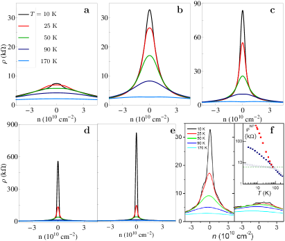
For the sake of comparison, we have reproduced in Fig. 1(f) the corresponding experimental results from Ref. [Ponomarenko_arX11, ]. The agreement between our calculated theoretical results and the experimental data is striking: In the presence of substantial (vanishing) electron-hole puddles characterized by larger (smaller) values of the disorder fluctuation parameter , the calculated saturates (increases monotonically) at lower average carrier density exactly as observed experimentally in the presence (absence) of the puddles. We emphasize that the theoretical results obtained in Fig. 1 use exactly the same parameters for all cases except for varying the value of the potential fluctuation parameter ‘’ as given in the figure (which mimics the effect of the suppression of through screening by the second graphene layer in Ref. [Ponomarenko_arX11, ]). One interesting prediction of our theory is that never truly diverges as in our theory as (unless exactly, which is unphysical) since there is always a low-density cut-off defining the conductivity minimum regime with decreasing with decreasing . This low-density cut-off (and the corresponding “maximum resistivity” ) depends strongly on the puddle parameter ‘’ – the suppression of ‘’ dramatically increases (decreases) .
Before discussing our results for the temperature dependence of the resistivity , we briefly discuss our transport theory Adam_PNAS07 ; dassarma2010 ; HwangAdamDas_PRL07 ; rossi2008 ; Hwang_InsuPRB2010 for graphene conductivity in the presence of electron-hole puddle induced strong density inhomogeneity. The conductivity is obtained by using the effective medium theory (EMT) by solving the integral equation
| (2) |
where is the effective conductivity of the sample and is the density dependent local conductivity with the carrier density having the distribution defining the electron-hole puddles – here is the average density defined by the external gate voltage (i.e., at the charge neutral Dirac point) and is the root-mean-square density fluctuation due to the existence of density inhomogeneity associated with the puddles. We calculate using the finite-temperature Boltzmann-RPA transport theory using screened random quenched charged impurity centers (of 2D concentration ) in the environment as the resistive scattering mechanism. The Boltzmann transport theory, which has been described in details elsewheredassarma2010 ; HwangAdamDas_PRL07 ; Hwang_InsuPRB2010 ; HwangScreen_PRB09 , includes five distinct temperature-dependent contributions: (1) thermal activation of electron-hole occupancy (i.e. thermal excitation of electrons from the valence band to the conduction band); (2) finite temperature thermal averaging around the Fermi surface according to the Fermi distribution function; (3) the thermal activation of carriers over the potential fluctuations associated with the electron-hole puddles; (4) finite temperature screening by the carriers themselves; (5) phonon effects (which are straightforward to includeHwangDasPhonon_PRB08 , but are neglected here since electron-phonon coupling is weak in graphene). The thermal effects (1)-(3) above produce ‘insulating’ temperature dependence, i.e., the temperature-dependent resistivity increases with decreasing , whereas the last two effects lead to a ‘metallic’ decreasing with decreasing temperature. All the thermal effects are suppressed with increasing carrier density (or more precisely, increasing ), and they are the strongest at the charge neutral Dirac point (where the nominal vanishes). We note that in our figures, whereas the density , i.e., the average density.
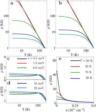
In Fig. 2 we depict our calculated at fixed including puddle effects (characterized by the parameter ) within the Boltzmann transport theory as described above (and elsewhereHwang_InsuPRB2010 ; HwangScreen_PRB09 ). The calculated temperature dependent resistivity is identical to the experimental observations of Ref. [Ponomarenko_arX11, ], as reproduced in our Fig. 1(f), with the Dirac point resistivity increasing strongly with lowering temperature for smaller values of (i.e., when the potential fluctuations associated with the electron-hole puddles are strongly suppressed) whereas the resistivity at high carrier density manifesting almost temperature-independent behavior. We emphasize, however, that within our semiclassical transport theory, in spite of the very strong increase of the Dirac point with lowering for small , eventually saturates at some large -dependent (and -dependent) value at low enough even at the Dirac point – empirically we find that at the Dirac point saturates for . Then, the Dirac point behavior of for different values of is qualitatively similar if plotted as a function of . Therefore, one clear prediction of our semiclassical theory is that at low enough temperatures the experimentally measured will always saturate even at the Dirac point, but the crossover temperature for this saturation would be very low when the electron-hole puddles are strongly suppressed. Thus, in our theory would behave very much like a density-tuned metal-insulator transition, as observed in Ref. [Ponomarenko_arX11, ], for all practical purposes except that the temperature dependence would be a power law (and not an exponential as in a strongly localized system), exactly as seen in Ref. [Ponomarenko_arX11, ].
III Discussion
One point we should make clear here about the “disorder by order” phenomenon is that it arises from the suppression of the electron-hole puddles associated with the density inhomogeneity around the Dirac point induced by Coulomb disorder, and not simply from an impurity-induced collisional broadening effect in the graphene density of states. In particular, one may wonder whether the impurity broadening effect leading to a finite carrier density of states at the Dirac point could by itself lead to the disorder by order phenomenon since this would imply that a cleaner system would have a lower density of states at the Dirac point and hence a higher resistivity. While this is certainly true in general, i.e. when a material exhibits a density of states minimum, addition of disorder leads to an increased density of states near this minimum due to smearing which then leads to a higher Drude conductivity, this is not the primary operational mechanism for the disorder by order phenomenon. As we show in Appendix A of this paper, such an enhanced disorder-broadened density of states indeed leads to higher conductivity near the Dirac point for more disordered graphene samples, but the conductivity always vanishes at the Dirac point () in this situation as long as Coulomb disorder (i.e. random charged impurities in the environment) is present in the system independent of whether the density of states is zero or finite at the Dirac point. In our proposed order by disorder mechanism, by contrast, the conductivity is always finite at the Dirac point because of the disorder-induced inhomogeneous puddles except that this finite minimum Dirac point conductivity arising from the puddles is much lower for the more ordered systems than it is for the more disordered systems while the reverse is true at high density. Thus, the presence (suppression) of puddles is the important physics in our disorder by order mechanism, not the disorder-induced smearing of the graphene density of states around the Dirac point. We discuss the issue of the density of states smearing effect on the graphene conductivity in Appendix A.
Before concluding, we now provide a critical discussion of our theory as applied to the experimental observations of Ref. [Ponomarenko_arX11, ]. This issue is discussed in details in Appendix B. First, our results provide an excellent description of the experimental observations with respect to the dependence of the measured resistivity as a function of carrier density, temperature, and disorder associated with the electron-hole puddles. Indeed, the agreement between our theory and the experimental data is striking, lending credence to our claim that the observation of Ref. [Ponomarenko_arX11, ] is an experimental verification of our predicted “disorder by order” phenomenon in monolayer grapheneFootNote . In Ref. [Ponomarenko_arX11, ], the potential fluctuations associated with electron-hole puddles in the graphene layer were suppressed by a second close-by graphene layer with a very high carrier concentration. We have verified by direct numerical simulations that such a suppression can indeed be caused by the second high-density graphene layer separated by a distance acting as a gate which screens the potential fluctuations reducing them substantially below their pristine value arising from the random charged impurity distribution. A simple electrostatic analytic calculation shows that the suppression of would be approximately by a factor when . For cm-1 and nm, could thus be suppressed by a factor as large as ! Thus our basic picture of the suppression of the potential fluctuation parameter ‘’ leading to the disorder by order phenomenon at the Dirac point is applicable to Ref. [Ponomarenko_arX11, ]. In Ref. [Ponomarenko_arX11, ], it is also found that the disorder-by-order phenomenon is itself suppressed by the application of a weak magnetic field mT. Although the inclusion of a magnetic field in the theory is beyond the scope of the current work, we mention that a magnetic field mT corresponds to a minimum Landau level energy separation meV which is comparable to for cm-2. Thus, a mT magnetic field is not a weak field at the Dirac point, which would nonperturbatively modify the physics, considerably suppressing the disorder by order phenomenon.
We believe that the disorder by order phenomenon should occur in any Dirac material with chiral gapless linear energy spectrum as long as quantum interference effects are negligible, and as such, we predict the existence of the same phenomenon in the 2D surface transportCulcerFuhrer in 3D topological insulators provided that the surface puddles are suppressed in the system and the temperature is not too low. In fact, all gapless semiconductors will manifest the disorder by order phenomenon if impurity-induced potential fluctuations can be suppressed in the low carrier density regime. Indeed, we believe that some earlier graphene experiments BolotinDu_Sus08 observing anomalous temperature dependence of the Dirac point resistivity are observing exactly the same disorder-by-order phenomenon as reported in Ref. [Ponomarenko_arX11, ] except that the authors of Ref. [BolotinDu_Sus08, ] interpret their observations as ballistic transport whereas Ponomarenko et al. Ponomarenko_arX11 invoke Anderson localization!
IV Conclusion
We conclude by emphasizing that the recently observed intriguing phenomenon Ponomarenko_arX11 of monotonically increasing graphene resistivity with decreasing carrier density in graphene samples of very high purity (with very high mobilities at high carrier densities) most likely arises not from Anderson localization, but from the semiclassical “disorder by order” phenomenon proposed in the current manuscript. This phenomenon arises from the suppression of electron-hole puddles in the system by a near-by screening layer which then induces the system to show its intrinsic Drude behavior of the resistivity being inversely proportional to the carrier density down to much lower carrier densities without being cut off by the puddle-induced (and well-known Adam_PNAS07 ; dassarma2010 ; rossi2008 ; Hwang_InsuPRB2010 ) “graphene conductivity minimum” mechanism. The qualitative difference between our “disorder by order” mechanism and localization is that in our case, the conductivity is always finite, eventually being cut off by remnant puddles in the system at much lower carrier densities determined by the details of disorder and screening by the second layer whereas in for localization the conductivity is truly zero at . The other qualitative difference is that the predicted temperature dependence of the resistivity at a fixed low carrier density near the Dirac point in our mechanism is a power law whereas it must be exponential in the case of Anderson localization. The observed temperature and density dependence of the low-density resistivity in Ref. [Ponomarenko_arX11, ] is consistent with our predictions, and hence we believe that Ref. [Ponomarenko_arX11, ] is manifesting the “disorder by order” phenomenon, not Anderson localization. When and how graphene can manifest localization (as opposed to antilocalization, which is the expected behavior for graphene) is an interesting question for the future, but we believe that the experimental temperature range must be much lower than that used ( K) in Ref. [Ponomarenko_arX11, ] to see any quantum interference induced localization effects since the inelastic phase coherence length is simply too short (Appendix B) for localization effects to manifest at higher temperatures. We urge transport experiments in high quality graphene at very low temperatures ( K) to discern localization/antilocalization versus semiclassical “disorder by order” puddle effects.
Acknowledgements.
This work is supported by US-ONR-MURI and NRI-SWAN. One of the authors (SDS) gratefully thanks Andre Geim for stimulating discussions and helpful comments.Appendix A
The density of states (DOS) of disordered graphene is calculated within the self-consistent Born approximation (SCBA). In calculating the DOS only a short range disorder potential is considered. The conductivity is calculated with a simple formula
| (3) |
where is the DOS at Fermi level, and is the transport scattering time. Note that the scattering time is calculated with the DOS of the bare band and with two different disorders, short range potential and long range Coulomb potential. Thus, the scattering time is given by
| (4) |
where () is the scattering time due to the long-range Coulomb impurities (short range impurities) and they are given by in the Boltzmann transport approach
| (5) |
where is the DOS of bare band. In low density limit, , the scattering rate by Coulomb impurities dominates and the total scattering time behaves as , i.e., . Thus, even though the DOS is finite at the conductivity, as .
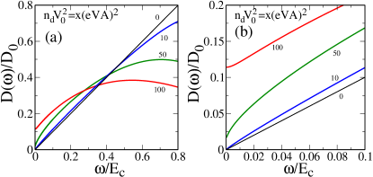
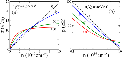
We calculate the disorder-broadened DOS for graphene following Refs. [hu2008, ], and then calculate the conductivity following Eqs. (3)–(5) above. Our results for the broadened DOS and the resulting conductivity are shown in Figs. 3 and 4. The important points to note are :(1) the disorder-broadened DOS leads to an enhanced (suppressed) conductivity at low (high) carrier densities for more (less) disordered systems in agreement with Ref. [Ponomarenko_arX11, ]; (2) but the Dirac point conductivity is always zero independent of whether the DOS is smeared by disorder or not and thus the smearing of the DOS by itself cannot be the explanation for the existence of the minimum conductivity plateau in graphene which necessitates the existence of electron-hole puddles in the system.
We can consider the DOS of disordered graphene (rather than the DOS of the bare graphene as done above) to calculate the scattering time. Now we have a finite DOS as . Then with the same approach as Eq. (5) we have the scattering times as
| (6) |
Similarly we have , and as .
Thus, the DOS smearing by disorder always produces zero conductivity at the Dirac point () in graphene although close to the Dirac point the smearing of the DOS does indeed lead to an enhanced conductivity as shown in the figures. Although our results are shown within the SCBA theory of the DOS smearing, the qualitative findings are the same within the simpler Born approximation where the disorder broadening of the DOS does not lead to a finite DOS at zero density. Thus, the DOS smearing by disorder cannot be an explanation for the graphene finite minimum conductivity around the Dirac point which arises from the Coulomb disorder induced density inhomogeneity and electron-hole puddles in the system.
Appendix B
In this Appendix, we tackle two important (and inter-related) questions: (i) What about Anderson localization? (ii) Can our Boltzmann theory be valid for ? We discuss these questions in some details below.
First, in the absence of inter-valley scattering graphene should manifest anti-localizationTheoryAntiLocal behavior for which there is some experimental evidence in some situationsExpAntiLocal . The presence of inter-valley scattering would restore the usual localization behaviorAleiner_PRL . But the crossover from the anti-localization behavior to the localization behavior should occur at an extremely low temperature comparable to the inter-valley scattering rate which is likely to be much less than K. It is therefore reasonable to assume that localization effects are operationalFootNote at much lower temperature scales than the results presented in this paper and that used in the experiments of Ref. [Ponomarenko_arX11, ]. In addition, the measurements of Ref. [Ponomarenko_arX11, ] are performed at high temperatures ( K) where quantum interference effects are strongly suppressed because the inelastic phase breaking length is shorter than the elastic mean free path. The validity of the Boltzmann theory is, as a matter of principle, completely independent of the resistivity of the system as long as quantum localization/interference effects can be neglected. Thus, our semiclassical theory does not simply care about the condition as long as quantum interference corrections are small which is true at high temperatures.
We discuss below the extent to which our semiclassical disorder-by-order transport phenomenon applies to the recent experimental observations of Ponomarenko et al. Ponomarenko_arX11 , who have interpreted their measured graphene resistivity in terms of an Anderson localization driven metal-insulator transition at low carrier density.
We believe that the data of Ref. [Ponomarenko_arX11, ] are inconsistent with quantum interference induced localization transition for the following reasons: (1) the temperature regime explored in Ponomarenko_arX11 is sufficiently high ( K) where localization effects should be strongly suppressed since the inelastic phase breaking length is comparable to or shorter than the elastic mean free path making quantum interference irrelevant; (2) the temperature dependence of the measured resistivity in Ref. [Ponomarenko_arX11, ] is not exponential and is thus inconsistent with Anderson localized insulating behavior; (3) the density dependence of the measured resistivity in Ref. [Ponomarenko_arX11, ] follows our predicted semiclassical behavior at low density (before it saturates at a very low temperature-dependent cut-off density near the Dirac point exactly as our semiclassical theory predicts)– this is hard to reconcile with Anderson localization; (4) there is no observable weak localization (or anti-localization) behavior manifesting in the data at high density where the resistivity is low (and weak localization corrections should be discernible if indeed a density-tuned metal-insulator strong localization phenomenon is taking place); (5) graphene can manifest true localization (even at ) only in the presence of intervalley scattering which is generally known to be extremely weak (in the absence of intervalley scattering and trigonal warping, graphene can only manifest anti-localization– the experimental data of Ref. [Ponomarenko_arX11, ] do not directly exhibit any signature of strong inter-valley scattering, for example, the high-density resistivity is completely consistent with the intervalley scattering being weak); (6) the temperature scale for the strong localization transition should be lower than the characteristic (very low) energy scale for the intervalley scattering, but the experimental data of Ref. [Ponomarenko_arX11, ] manifest insulating-like behavior already at rather high ( K) temperatures, casting doubts on the whole metal-insulator transition picture; and finally (7) as emphasized in our main manuscript, our semiclassical theory is in excellent agreement with the observed experimental data of Ref. [Ponomarenko_arX11, ], and the observed data manifest no direct signature of quantum interference effects.
Having argued above that the experimental observations of Ponomarenko et al. Ponomarenko_arX11 are unlikely to be arising from a quantum strong localization induced metal-insulator transition, we now give the reasons for our firm belief that Ref. [Ponomarenko_arX11, ] is a direct manifestation of our predicted semiclassical “disorder by order” phenomenon: (1) our theoretical results provide an excellent quantitative description of the experimentally measured resistivity; (2) the density and the temperature dependence of the resistivity in Ref. [Ponomarenko_arX11, ] follows precisely the asymptotic and behavior predicted in our theory; (3) we predict the correct disorder dependence, i.e., lower the puddle induced inhomogeneity or potential fluctuation, stronger is the low-density insulating behavior; (4) our theory provides a clear qualitative and quantitative explanation for why the inhomogeneous electron-hole puddles must be suppressed in order to observe the apparent low-density insulating behavior; (5) our theory can explain the data both in the presence and in the absence of the puddles (with the low-density insulating behavior being respectively absent and present) whereas in the quantum localization scenario no explanation is available for the generic situation in the presence of puddles– one must assert ad hoc that the presence of puddles somehow hinders the localization effect; (6) in the high temperature regime explored in Ref. [Ponomarenko_arX11, ], quantum interference effects are strongly suppressed making our semiclassical theory applicable – we emphasize that quantum interference cannot occur if the phase coherence length is short as it is in the temperature regime of Ref. [Ponomarenko_arX11, ].
We come to the purely theoretical (rather than empirical) question of the applicability of our semiclassical theory to the experimental situation of Ref. [Ponomarenko_arX11, ] where the measured resistivity is high () so that the well-known localization condition (which is equivalent to the condition written out in terms of Fermi wavevector and mean free path) is violated, and the low-density insulating phase in Ref. [Ponomarenko_arX11, ] actually corresponds to regime, where is the elastic (or transport) mean free path, given by , where is the appropriate finite-temperature elastic scattering time due to Coulomb disorder. It is indeed true that is approximately the condition (“the Ioffe-Regel criterion”) for localization effects to become important in an electronic system with the regime being dominated by quantum interference induced localization effects where semiclassical transport theory should be nominally invalid since localization corrections to the resistivity should become larger that the semiclassical resistivity itself. This is, however, true only at (or at extremely low temperatures) where with being the inelastic phase coherence length for the electrons (at , , and the condition is trivially satisfied). Thus, quantum localization requires a necessary condition () so that quantum interference is operational and a sufficient condition (, where is the Fermi wavelength). Without the necessary condition () being satisfied, quantum interference is simply not operational in a given experimental situation. (This is the reason that quantum localization phenomenon is typically experimentally studied at very low mK range of temperatures, not at K.)
The necessary condition () for quantum interference (i.e., localization) to be operational is not satisfied by the experimental conditions ( K) used in Ref. [Ponomarenko_arX11, ]. In particular, we have calculated qzli_inelastic the inelastic phase breaking length due to electron-electron and electron-phonon interactions in graphene, finding that typically in the higher temperature ( K) regime used in Ref. [Ponomarenko_arX11, ], and even at the lowest measurement temperature in Ref. [Ponomarenko_arX11, ], K, . Our theoretical results for will be published elsewhere qzli_inelastic , but we mention that our finding that in the experimental regime of Ref. [Ponomarenko_arX11, ] is consistent with the available direct experimental measurements of in graphene. For example, Ref. [Ponomarenko_arX11, ] specifically quotes m at liquid helium temperature ( K), which translates into Å for K since in graphene due to the dominant electron-electron interaction qzli_inelastic . The actual values of may even be smaller because of disorder effects and electron-phonon interactions. Direct measurements of in graphene Savchenko_PRL08 are consistent with our estimate that in most of the temperature regime explored in Ref. [Ponomarenko_arX11, ]. Thus, quantum interference phenomena are unlikely to be playing any role in Ref. [Ponomarenko_arX11, ] except perhaps at the lowest temperatures ( K).
It will be desirable for the experimental regime of Ref. [Ponomarenko_arX11, ] to be pushed down well below K ( K) where the necessary condition for quantum interference to be operational, namely, , should apply. We expect our theory to fail in this low-temperature interference-dominated puddle-free regime, and it will be extremely interesting to study the deviations of the experimental data from our semi-classical theory in this low temperature ( K) regime so as to learn about the nature of graphene localization. We believe, for reasons discussed above, that the current experimental data of Ref. [Ponomarenko_arX11, ] fall in the intriguing regime of and where our semiclassical theory still remains valid.
We point out a technical issue which makes our theory even more applicable to the measurements in Ref. [Ponomarenko_arX11, ] than the above discussion implies. The elastic scattering length that should be compared to (so as to check if condition is satisfied for quantum interference to be relevant) is not the net mean free path defining the resistivity, but only the inter-valley scattering length . This is because most of the elastic resistive scattering in graphene is intravalley scattering which cannot lead to Anderson localization (in fact, it should induce anti-localization TheoryAntiLocal ). Since the actual inter-valley scattering is very weak, according to Ref. [Ponomarenko_arX11, ], m, we conclude that the experimental situation in Ref. [Ponomarenko_arX11, ] corresponds entirely to the regime in the K range since and therefore Å throughout the temperature range studied in Ref. [Ponomarenko_arX11, ]. Basically, the experimental conditions in Ref. [Ponomarenko_arX11, ] correspond more to the infinite temperature limit than the zero temperature limit as far as quantum interference effects are concerned and as such our semiclassical theory should apply well to Ref. [Ponomarenko_arX11, ]. We therefore believe that the current data of Ref. [Ponomarenko_arX11, ] are well-explained by our theory to be a semiclassical disorder by order phenomenon.
We conclude by noting that in addition to the semiclassical disorder by order and the localization induced metal insulator transition phenomena, in principle there is a third possible explanation for the low-density insulating behavior observed by Ponomarenko et al. Ponomarenko_arX11 . This is the possibility of a spontaneous interaction-induced gap formation at the Dirac point Drut_arXiv , which would of course lead to the insulating behavior when the chemical potential approaches the gap at low density (similar to ordinary semiconductors). This gap scenario is unlikely to be operational in the experiment of Ref. [Ponomarenko_arX11, ] because (1) typically the predicted spontaneous gap is very small, much less than the temperature range ( K) explored in Ref. [Ponomarenko_arX11, ], and (2) the temperature dependence of the resistivity in Ref. [Ponomarenko_arX11, ] is a power law (roughly ) which is inconsistent with the exponentially activated resistivity expected for a gapped system. Again, experiments need to be carried out at much lower temperatures (below K) for a thorough investigation of this issue of the spontaneous gap formation, which has recently been controversial in the literature with different theories claiming both the existence and the nonexistence of an interaction-induced graphene gap formation Drut_PRL09 .
References
- (1) L. A. Ponomarenko, A. K. Geim, A. A. Zhukov, R. Jalil, S. V. Morozov, K. S. Novoselov, I. V. Grigorieva, E. H. Hill, V. V. Cheianov, V. I. Fal’ko, K. Watanabe, T. Taniguchi, and R. V. Gorbachev, Nat. Phys. 7, 958 (2011)
- (2) S. Adam, E. H. Hwang, V. M. Galitski, and S. Das Sarma, Proc. Natl. Acad. Sci. USA 104, 18392 (2007); V. Cheianov, V. I. Fal’ko, B. L. Altshuler, and I. L. Aleiner, Phys. Rev. Lett. 99, 176801 (2007)
- (3) J. Martin, N. Akerman, G. Ulbricht, T.Lohmann, J. H. Smet, K. V. Klitzing, and A.Yacoby, Nat. Phys. 4, 144 (2008); Y. Zhang, V. W. Brar, C. Girit, A. Zettl, and M. F. Crommie, Nat. Phys. 5, 722 (2009); A. Deshpande, W. Bao, F. Miao, C. N. Lau, and B. J. LeRoy, Phys. Rev. B 79, 205411 (2009)
- (4) S. Das Sarma, S. Adam, E. H. Hwang, and E. Rossi, Rev. Mod. Phys. 83, 407 (2011); N. M. R. Peres, Rev. Mod. Phys. 82, 2673 (2010)
- (5) E. H. Hwang, S. Adam, and S. Das Sarma, Phys. Rev. Lett. 98, 186806 (2007)
- (6) K. Nomura and A. H. MacDonald, Phys. Rev. Lett. 98, 076602 (2007)
- (7) T. Ando, J. Phys. Soc. Jpn. 75, 074716 (2006)
- (8) J. H. Chen, C. Jang, S. Adam, M. Fuhrer, E. D. Williams, and M. Ishigami, Nature Phys. 4, 377 (2008); Y. W. Tan et al., Phys. Rev. Lett. 99, 246803 (2007); J. Heo et al., Phys. Rev. B 84, 035421 (2011); W. Zhu et al., Phys. Rev. B 80, 235402 (2009); C. Jang et al., Phys. Rev. Lett. 101, 146805 (2008); S. Adam et al., Phys. Rev. Lett. 101, 046404 (2008); A. K. M. Newaz, et al., Nat. Commun. 3, 734 (2012)
- (9) K. S. Novoselov, A. K. Geim, S. V. Morozov, D. Jiang, Y. Zhang, S. V. Dubonos, I. V. Grigorieva, and A. A. Firsov, Science 306, 666 (2004); K. S. Novoselov, D. Jiang, F. Schedin, T. J. Booth, V. V. Khotkevich, S. V. Morozov, and A. K. Geim, Proc. Natl. Acad. Sci. USA 102, 10451 (2005); K. S. Novoselov, A. K. Geim, S. V. Morozov, D. Jiang, M. I. Katsnelson, I. V. Grigorieva, S. V. Dubonos, and A. A. Firsov, Nature 438, 197 (2005)
- (10) E. Rossi and S. Das Sarma, Phys. Rev. Lett. 101, 166803 (2008); E. Rossi, S. Adam, and S. Das Sarma, Phys. Rev. B 79, 245423 (2009)
- (11) E. H. Hwang and S. Das Sarma, Phys. Rev. B 82, 081409 (2010); Q. Li, E. H. Hwang, and S. Das Sarma, Phys. Rev. B 84, 115442 (2011)
- (12) E. H. Hwang and S. Das Sarma, Phys. Rev. B 79, 165404 (2009); M. Müller, M. Bräuninger, and B. Trauzettel, Phys. Rev. Lett. 103, 196801 (2009)
- (13) E. H. Hwang and S. Das Sarma, Phys. Rev. B 77, 115449 (2008); Hongki Min, E. H. Hwang, and S. Das Sarma, Phys. Rev. B 83, 161404 (2011)
- (14) A compelling point in this context is that the analytical prediction of our theory at the Dirac point, for , is obeyed well both by our numerical results and by the experimental data of Ref. [Ponomarenko_arX11, ], arguing in favor of the disorder by order phenomenon being operational in the experimental observation in contrast to some other mechanism, e.g. localization, which typically leads to exponential -dependence in the resistivity.
- (15) D. Culcer, E. H. Hwang, T. D. Stanescu, and S. Das Sarma, Phys. Rev. B 82, 155457 (2010); D. Kim, S. Cho, N. P. Butch, P. Syers, K. Kirshenbaum, S. Adam, J. Paglione, and M. S. Fuhrer, Nat. Phys. (in press)
- (16) K. I. Bolotin, K. J. Sikes, J. Hone, H. L. Stormer, and P. Kim, Phys. Rev. Lett. 101, 096802 (2008);X. Du, I. Skachko, A. Barker, and E. Y. Andrei, Nat. Nanotech. 3, 491 (2008)
- (17) B. Y. K. Hu, E. H. Hwang, and S. D. Sarma, Phys. Rev. B 78, 165411 (2008); B. Dora, Klass Ziegler, and Peter Thalmeier, Phys. Rev. B 77, 115422 (2008); P. M. Ostrovsky, I. V. Gornyi, and A. D. Mirlin, Phys. Rev. B 74, 235443 (2006)
- (18) H. Suzuura and T. Ando, Phys. Rev. Lett. 89, 266603 (2002); E. McCann, K. Kechedzhi, V. I. Fal’ko, H. Suzuura, T. Ando, and B. L. Altshuler, Phys. Rev. Lett. 97, 146805 (2006); A. F. Morpurgo, and F. Guinea, Phys. Rev. Lett. 97, 196804 (2006); S. V. Morozov, K. S. Novoselov, M. I. Katsnelson, F. Schedin, L. A. Ponomarenko, D. Jiang, and A. K. Geim, Phys. Rev. Lett. 97, 016801 (2006); D. V. Khveshchenko, Phys. Rev. Lett. 97, 036802 (2006)
- (19) X. Wu, X. Li, Z. Song, C. Berger, and W. A. de Heer, Phys. Rev. Lett. 98, 136801 (2007); F. V. Tikhonenko, A. A. Kozikov, A. K. Savchenko, and R. V. Gorbachev, Phys. Rev. Lett. 103, 226801 (2009)
- (20) I. L. Aleiner and K. B. Efetov, Phys. Rev. Lett. 97, 236801 (2006)
- (21) S. Das Sarma and Q. Li, unpublished
- (22) F. V. Tikhonenko, D. W. Horsell, R. V. Gorbachev, and A. K. Savchenko, Phys. Rev. Lett. 100, 056802 (2008); D. Ki, D. Jeong, J. Choi, and H. Lee, Phys. Rev. B 78, 125409 (2008)
- (23) J. E. Drut, T. A. Lähde, and E. Tölö, arXiv:1005.5089 (2010)
- (24) J. E. Drut and T. A. Lähde, Phys. Rev. Lett. 102, 026802 (2009); J. Wang, and G. Liu, New J. Phys. 14, 043036 (2012)