Fano Mechanism of the Giant Magnetoresistance Formation in a Spin Nanostructure
Abstract
It is shown that, upon the electron quantum transport via the nanostructure containing a spin dimer, the spin-flip processes caused by the s-f exchange interaction between electron and dimer spins lead to the Fano resonance effects. An applied magnetic field eliminates degeneracy of the upper triplet states of the dimer, changes the conditions for implementation of the Fano resonances and antiresonances, and induces the new Fano resonance and antiresonance. It results in the occurrence of a sharp peak and dip in the energy dependence of transmittance. These effects strongly modify the current–voltage characteristic of the spin-dimer structure in a magnetic field and form giant magnetoresistance.
- PACS numbers
-
73.23.-b, 73.63.Nm, 75.47.De, 75.76.+j, 71.70.Gm
pacs:
Valid PACS appear hereIn recent years, molecular compounds have been considered as promising basis nanoelectronic elements playing an important role in quantum transport Fagas . The exchange interaction between spin moments of a conduction electron and a molecule induces additional effects in the spin-polarized transport via magnetic molecules. Among these effects are quantum tunneling of magnetization of a molecule Mis and the Kondo effect Liang . Such molecular compounds can exhibit strong magnetic anisotropy sufficient to support stable orientation of the spin at low temperatures Gatt . Therefore, along with magnetic nanoheterostructures Ved ; Gul ; Mir , magnetic molecular and atomic systems are currently considered as memory elements. In view of this, the account for the electron-electron Del and electron-phonon Tikh ; Ars interactions, which cause phase mismatch of conduction electrons upon quantum transport, takes on great significance.
In addition to the mentioned features, it should be taken into consideration that, upon coherent quantum transport via molecular compounds, the transport properties of the latter can exhibit the features related to the interference resonance between the states of continuum and the states of a discrete spectrum (Fano resonance) Fano . Currently, many resonance phenomena for a great number of physical systems with discrete energy levels in the continuum energy band are described well by the Fano formula (see, for example, review Kivshar ).
On this basis, it is reasonable to expect that spin degrees of freedom and interactions between them offer new opportunities for implementation of the Fano resonance phenomena in the coherent spin-polarized transport via a spin nanostructure. One can suggest that such resonance effects upon strong correlation between charge and spin degrees of freedom manifest themselves, for example, in giant magnetoresistance. The aim of this study was to confirm the above statements by an example of the calculation of current–voltage characteristics for a spacer containing magnetoactive ions grouped in spin dimers.
Consider a one-electron spin-polarized current via the region containing a spin structure in the form of a spin dimer connected with one-dimensional metal electrodes (Fig.1). Such a geometry of the problem corresponds to the case when the active region represents an extremely thin layer of the material prepared on the basis of a quasi-one-dimensional antiferromagnet, in which chains of magnetic ions strongly coupled by the exchange interaction are oriented perpendicular to the layer plane. This situation is limit because a number of magnetic ions in a chain is two, i. e., the dimer is formed.
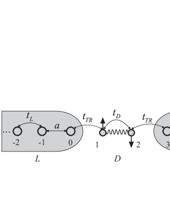
The antiferromagnet is quasi-one-dimensional, which is revealed in a negligibly small coupling of the spin dimers with one another. Then, within the strong coupling method, hoppings in the directions perpendicular to the dimer axis can be neglected, so the electron transport becomes one-dimensional (Fig.1).
Electron passage via the spin dimer structure exhibits the features caused by the s-f exchange interaction between the spin of a transferred electron and the spins of magnetoactive ions. This is due to the fact that the s-f interaction not only induces a potential profile of an electron flying throughout the structure but also changes this profile by means of the spin-flip processes. In this case, as will be shown below, resonance effects closely related to the Fano effect can occur; their characteristics, however, are directly related to the presence of spin degrees of freedom in the system. Owing to this fact, it becomes possible to attain giant values of magnetoresistance based on the Fano resonance arising during the electron transport via a quasi-molecular spin structure, which forms a potential profile for the transferred electron depending on spin configuration of the structure.
Below we will assume, as often, that the electrodes are connected with reservoirs that are macroscopic conductors. Then, electrons are thermalized and their temperature and chemical potential coincide with those of the contact before their return to the device, i. e., the contacts are considered to be reflectionless and the electrodes, to be ideal Bruus . Over the entire chain length, distance between sites is assumed to be invariable.
We write the Hamiltonian of the system in the form
| (1) |
where two first terms correspond to the electron Hamiltonians of the left () and right () electrodes, which are expressed in the secondary quantization representation as
where () is the creation (annihilation) operator for a conduction electron with spin on site of electrode (); is the one-electron spin-dependent energy on the site of electrode in external magnetic field , and is the hopping integral (the same for both electrodes). The axis along which the magnetic field is directed is perpendicular to the direction of electron motion. The third term in expression (1) describes hoppings of a conduction electron between the device and the contacts:
and the fourth term of the Hamiltonian reflects the processes of electron motion in the device:
The interaction between the transferred electron and the dimer spins is determined by the term
| (2) |
Here, is the parameter of the s-f exchange interaction and and are the operators of the spin moment entering the dimer structure and located on site .
Operator in expression (1) describes the exchange interaction between the dimer spin moments and their energy in magnetic field :
| (3) |
where is the parameter of the exchange interaction. Below, we will consider the case of a weak magnetic field (); therefore, the singlet state will be the ground state of the dimer. The last term in the Hamiltonian characterizes the potential energy of an electron in an electric field. It is assumed that there is the potential jump between the dimer sites such that and .
In solving the Schrodinger equation, due to the presence of the s-f exchange interaction, one must take into account the states with different spin projections for both the transferred electron an the dimer. As basis states, we choose the states characterizing the spin state of the transferred electron on site and one of the four states of the spin dimer: ; describes the singlet state of the dimer and , and describe its triplet states with , and , respectively. Here is the vacuum state for the fermion subsystem.
Let us consider the case when the electron approaching the device from the left contact has the spin projection and the spin dimer is in the singlet state . Then, the wave function of the system is written as
| (4) |
For the electron injected by the left contact with wave vector , the expansion coefficients in the left and right contacts has the form
| (5) | |||
where and are the reflection (transmission) amplitudes when the dimer is in the singlet and triplet states, respectively, and , and are the wave vectors satisfying the relations
| (6) | |||
These relations are written with the change in electron energy count by the value and on the assumption that the left and right conductors are identical. In the absence of bias voltage, , , and .
From the Schrodinger equation, we obtain the set of 12 equations for six reflection and transmission amplitudes and six coefficients , and . After certain transformations, this system is reduced to the three equations containing only the transmission amplitudes and, at , has the form
| (7) | |||
where , , . Hereinafter, all the energy quantities will be measured in the bandwidth units .
We limit the consideration to the low-energy region (), where the electron transport is implemented along one channel, since the kinetic energy of an electron is insufficient to transfer the dimer to the triplet states. This energy range is of interest because within this range, as will be shown below, the Fano resonance effects occur that allow implementation of giant magnetoresistance.
At , transmittance is determined only by amplitude : . Therefore, solving set (Fano Mechanism of the Giant Magnetoresistance Formation in a Spin Nanostructure), we arrive at
| (8) |
where
| (9) | |||
At zero magnetic field, , the transmittance is written in the simpler form
| (10) |
Here, we use the following notation:
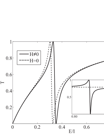
The energy dependence of transmittance at is shown in Fig.2 by the dotted line. It can be seen that the monotonic growth of with increasing kinetic energy of electron from zero value is changed for the splash of up to the maximum value and the sharp drop down to the zero value. After that, the dependence monotonically increases again. Total transmission and total reflection correspond to the Fano resonance and antiresonance Fano and are related to interference of the continuous spectrum states and discrete spectrum states. The energy value at which the antiresonance occurs is found from the condition of vanishing :
| (11) |
Near the same value, the Fano resonance is located at .
In a magnetic field, the triplet states of the spin dimer are split, which shifts the values of the discrete spectrum energies. Therefore, apart from the shift of the above-mentioned Fano resonance and antiresonance points (solid curve in Fig.2), at the new, magnetic-field-induced Fano resonance and antiresonance can occur. In Figure 2, this effect is revealed in the very narrow peak and dip of the dependence in the vicinity of . The magnetic-field-induced Fano resonance and antiresonance is enlarged in the insert in Fig. 2.
Mathematically, the above statements follow from the analysis of the expression for at . For the , the transmittance can be expressed as
| (12) |
where
The specific form of , and can be easily obtained from comparison of expressions (8) and (12); however, in our case, it is not important. It is significant only that the condition imposed on the magnetic-field-induced Fano antiresonance acquires the form
| (13) |
If , this condition is met at or at . However, the second equation does not lead to the antiresonance, since there are the same factors in the denominator of (12).
If , then, due to the difference in the expressions for , and , there are no reducible factors and the second solution can be implemented. This corresponds to inducing the Fano resonance and antiresonance by a magnetic field.
To sum up at the end of this section, note that the formation of the Fano resonance effects in this system is due to the spin-flip processes, since, as the calculation showed, there are no resonance effects when the exchange couplings are described by the Ising (not Heisenberg) Hamiltonians.
In order to calculate the current–voltage characteristic, we use the Landauer–Buttiker method Bruus ; Datta . Within this method, the dependence of current on applied voltage is determined by the well-known expression
| (14) |
where and are the Fermi functions of the electron distribution in the left and right contacts with the electrochemical potentials and , respectively; is the above-mentioned transmittance for the electron injected from the left electrode; and is the transmittance for the electron transferred from the right electrode. The coefficients and are calculated similarly.
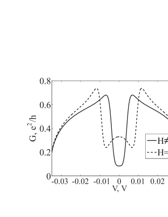
Figure 3 demonstrates the variation in the dependence of the differential conductance measured in the conduction quantum () units on bias voltage at the switched magnetic field. The parameters of the system are such that at the electron energies giving the main contribution to conductance are localized near the antiresonance on the right. With increasing , the antiresonance becomes more pronounced and conductance drops. With a further increase in , the Fano resonance starts contributing; correspondingly, the differential conductance (dotted line) becomes nonmonotonic.
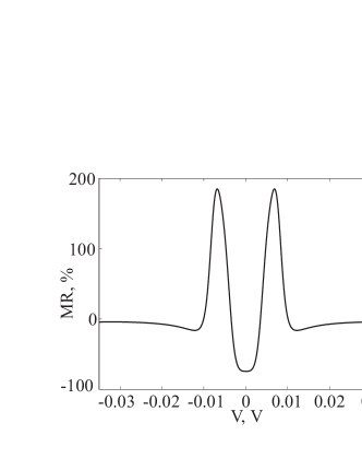
Switching off the magnetic field shifts the Fano resonance and antiresonance (Fig. 2). The magnetic field may appear such that the transmittance at is minimum (the Fano antiresonance case). It results in such a modification of the dependence of the differential conductance on bias voltage that at the switched magnetic field, in the region of small , the maximum changes for the minimum (solid curve in Fig. 3). These effects cause the occurrence of the large magnetoresistance at the switched magnetic field. The bias dependence of magnetoresistance is presented in Fig. 4. This result clearly demonstrates the possibility of attaining large magnetoresistance values by shifting the Fano resonance and antiresonance in the magnetic field. Magnetoresistance can take negative values.
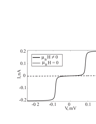
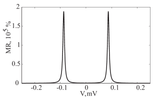
The magnetic-field-induced Fano resonance can cause abnormally large magnetoresistance values. Of the most interest is the case when the characteristic electron energies determining the resistive characteristics were localized in the vicinity of the Fano resonance in zero magnetic field. The parameters of the system and the external magnetic field can be such that at the Fano resonance occurs. Then, one should expect the strong conductance growth. Figures 5 and 6 demonstrate the current–voltage characteristic and magnetoresistance for this case. The current jump at mV (solid line in Fig. 5) arises because the resonance energy state starts contributing to the current-carrying states. It can be seen that the resistance variation in the magnetic field can reach (Fig. 6).
In this study, as an active element located between the metal electrodes, we used a nanostructure containing a spin dimer. The s-f exchange interaction between the conduction electron spin and the dimer spins forms a potential profile that contains both the constant (the Ising part of the interaction) and fluctuating (transversal part of the Heisenberg form ) components. Owing to the fluctuating part of the interaction, the Fano resonance effects occur.
For practical application, two effects caused by the magnetic field are important. The first effect is related to the shift in the energy region of the Fano resonance and antiresonance. The second, brighter effect results from splitting of the upper high-spin states. Due to the occurrence of the modified energy values of the discrete states in the system, these split states of the discrete spectrum also exhibit interference. It results in induction of the new Fano resonance and antiresonance. These effects all together cause the large values of magnetoresistance. Since the above statements on the effect of magnetic field are general, one can expect that the analogous effects of the giant magnetoresistance formation take place in other spin nanostructures.
This study was supported by the Program of the Physical Sciences Division of the Russian Academy of Sciences; Federal target program Scientific and Pedagogical Personnel for Innovative Russia, 2009-2013; Siberian Branch of the Russian Academy of Sciences, interdisciplinary project no. 53; Russian Foundation for Basic Research, project no. 09-02-00127, no. 11-02-98007. One of authors (S.A.) would like to acknowledge the support of the grant MK-1300.2011.2 of the President of the Russian Federation.
References
- (1) G. Fagas, G. Cuniberti, K. Richter (eds.), Introducing Molecular Electronics (Lecture Notes in Physics) (Springer Verlag, Berlin, 2005).
- (2) M. Misiorny, and J. Barnas, Phys. Rev. B 75, 134425 (2007).
- (3) W. Liang et al., Nature 417, 722 (2002).
- (4) D. Gatteschi, R. Sessoli, J. Villain, Molecular nanomagnets (Oxford University Press, Oxford, 2006).
- (5) A.V. Vedyaev, Phys. Usp. 45, 1296 (2002).
- (6) Yu.V. Gulyaev et al., JETP 107, 1027 (2008).
- (7) V.L. Mironov et al., 52, 2297 (2010).
- (8) P. Delaney and J. C. Greer, Phys. Rev. Lett. 93, 036805 (2004).
- (9) T. Mii, S. G. Tikhodeev, and H. Ueba, Phys. Rev. B 68, 205406 (2003).
- (10) P.I. Arseev, and N.S. Maslova, Phys. Usp. 53, 1151 (2010).
- (11) U. Fano, Phys. Rev. 124, 1866 (1961).
- (12) A. E. Miroshnichenko, S. Flash, and Y. S. Kivshar, Rev. Mod. Phys. 82, 2257 (2010).
- (13) H. Bruus, K. Flensberg, Many-body quantum theory in condensed matter physics: An Introduction (Oxford University Press, Copenhagen, 2004).
- (14) S. Datta, Electronic transport in mesoscopic systems (Cambridge University Press, Cambridge, 1995).