Fermi Surface Reconstruction in CeTe2 Induced by
Charge Density Wave:
ARPES Study
Abstract
Electronic structures of a charge-density-wave (CDW) system CeTe2-xSbx (=0, 0.05) have been investigated by employing angle-resolved photoemission spectroscopy (ARPES). The observed Fermi surface (FS) agrees very well with the calculated FS for the undistorted CeTe2 both in shapes and sizes. The metallic states crossing the Fermi level () are observed in ARPES. The carriers near have mainly the Te(1) character, with the negligible contribution from Ce states to the CDW formation. The supercell (shadow) bands and the corresponding very weak FS’s are found to arise from band-folding due to the interaction with Ce-Te(2) layers. This work shows that the origin of the CDW formation in CeTe2 is the FS nesting and that the CDW modulation vector is along -X (X).
pacs:
79.60.-i, 71.45.Lr, 71.18.+y, 71.20.-bThe charge-density-wave (CDW) formation is one of the most interesting phenomena in solid state physics.Voit00 ; Kasuya00 ; Yokoya01 CeTe2 is known as a CDW system having a high CDW transition temperature of TCDW1000 K, and the CDW state in CeTe2 coexists with magnetism and also with superconductivity (TC=2.7 K) under pressure.Jungprb03 CeTe2 crystallizes in the quasi-two dimensional layered Cu2Sb-type tetragonal structure with two types of Te sites: Te(1) and Te(2). Te(1) atoms form planar square sheets, which are sandwiched along the axis by the corrugated double layers of Ce and Te(2) atoms (Fig. 1). The ionic configuration of CeTe2 is considered to be Ce3+Te(2)2-Te(1)1-, so that hole carriers are produced in Te(1) sheets.Kang06 Then the square net of Te(1) would be easily distorted by the Peierls-like mechanismBurdett83 due to the partial filling. Underneath this picture is the assumption of trivalent Ce3+ states.Kang04 Band-structure calculations indicate that the CDW instability occurs due to the nesting between the Fermi surfaces in Te(1) square sheets in the plane,Dimasi96 ; Kikuchi98 ; Shim04 which was supported experimentally.Stowe00b
Due to the difficulty in growing high-quality single crystals for the angle-resolved photoemission spectroscopy (ARPES) study, there have been only a few ARPES studies of CeTe2. A couple of works reported the Fermi surface (FS) topology in the CDW state of CeTe2, as well as that in a similar CDW system LaTe2, by using ARPES.Shin05 ; Ito07 ; Garcia07 Shin et. al.Shin05 reported that the FS topology of CeTe2 in the - plane is different from that of LaTe2.Garcia07 The small square FS centered around , predicted by band calculations, was not observed in ARPES. So they conjectured that the CDW gap is larger than meV, and that the magnitude of varies around the FS. This minimum value of meV is much larger than meV, found in another ARPES study.Kang06 The CDW distortion probed by TEMShin05 was somewhat different from that in the literature,Stowe00b which was attributed to the variation of the Te deficiency produced by different sample growth techniques. Ito et. al.Ito07 examined the FS along the axis, and observed a systematic intensity modulation in the spectral weight at FS.
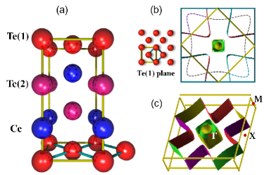
The natural question is whether the FS topology and the CDW state of CeTe2 are similar to those of LaTe2 or not. This includes the following issues: (i) do the FS and the CDW distorted structure in CeTe2 have the same symmetry as those in LaTe2?, (ii) how large is the effect of the band folding, due to the interaction between Te(1) and Ce-Te(2) layers, on the FS of Te(1) sheets?, and (iii) what is the CDW modulation vector, ? As shown in Fig. 1(b), the Brillouin Zone (BZ) of Te(1) sheets is reduced to half, and thereby, the bands are folded into the reduced BZ to yield the supercell (shadow) bands. The FS’s, denoted with dotted lines in Fig. 1(b), come from those shadow bands. We have resolved these questions by performing careful ARPES measurements for high-quality stoichiometric single crystals of CeTe2-xSbx (). We also report the detailed study of the FS topology, the energy-dependent behavior of the constant energy (CE) map, and the clearly dispersive feature of the states near the Fermi level () in CeTe2.
High-quality CeTe2-xSbx single crystals having very low residual resistivity were grown by using the self-fluxed Bridgeman method.BHM02 The quality and the orientation of the single crystal were checked by Laue patterns. ARPES experiments were carried out at the 3A1 beamline of the Pohang Light Source (PLS) with the beam size of m and using a Scienta SES-2002 electron energy analyzer. Single crystals were cleaved in situ at K under the pressure better than Torr, which exposed the (001) surfaces. The Fermi level and the overall instrumental resolution of the system were determined from the Fermi edge of an evaporated Cu metal. The energy resolution () and the momentum resolution () were set to be meV and , respectively, at eV.
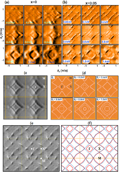
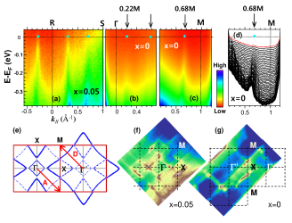
Figure 2 shows the first derivatives of the CE maps of CeTe2 (Left) and CeTe1.95Sb0.05 (Right) vs. the initial-state energy () of eV eV. These data were obtained at 30 K with 115 eV. In plotting each CE map, the spectral intensity of meV was integrated. This figure shows that the CE maps of =0 and =0.05 are essentially the same in their shapes, sizes, and energy-dependent behavior. But the CE maps of =0.05 are sharper than those of =0. Thus the energy-dependent evolution of the CE map is manifested more clearly in =0.05 than in =0.05
The four-fold symmetry is observed in the FSFS and CE maps for both =0 and 0.05. The feature of the four-fold symmetry is shown more clearly in the CE map for = eV (Fig. 2(c)), which was obtained from a different cleave. Two diamond-shaped contours are observed in the FS map, which is similar to the case of LaTe2.Garcia07 This finding implies that Ce electrons hardly contribute to the states near . Note that the inner-diamond FS is clearly seen in both =0 and 0.05, in contrast to the case of Ref.Shin05 . With increasing , the size of the inner diamond increases, while that of the outer diamond remains nearly the same. Such an energy-dependent behavior is consistent with that of the calculated FS’s, shown in Fig. 2(d).
Figure 2(e) shows the FS of CeTe1.95Sb0.05, drawn in the periodic zone scheme. This FS map was obtained by integrating the ARPES spectra for 50 meV (0 eV). The existence of the FS implies that there remain metallic states even below the CDW transition, producing the remnant ungapped FS. This conclusion is supported by the calculated FS, shown in Fig. 2(f). In Fig. 2(f), the experimental FS is compared with the calculated FS. The former is obtained by interpolating the partially ungapped FS’s and the latter is calculated for the non-CDW phase.Shim04 The experimental and calculated FS’s are very similar to each other in both sizes and shapes, supporting that the measured FS reflects the FS of the non-CDW phase of CeTe2. Two important features are noted here. First, this comparison confirms the FS nesting mechanism for the CDW formation in CeTe2. Secondly, the opening of the CDW gaps occurs only partially in some part of the FS, which is consistent with the semimetallic nature of CeTe2.Kang06 ; Lavagnini07 ; Lee08
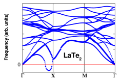
According to band calculations, there are two FS nesting vectors, one parallel to -X X), and the other parallel to -M M/2) for both LaTe2Kikuchi98 and CeTe2.Shim04 In general, is determined by the FS nesting vector.Dimasi96 In real systems, however, the CDW transition occurs only when there exists a soft phonon mode at a specific . In order to check the existence of a soft phonon mode in CeTe2, we have calculated the phonon dispersion for LaTe2 for simplicity.QE Indeed, the calculated (Fig. 3) exhibits negative values near X. This finding manifests phonon softening at X, and suggests that in CeTe2 corresponds to X, but not to M/2.
In Fig. 4, we have compared the ARPES intensity plots of CeTe2 with the band structures, calculated for the non-CDW lattice.Jwkim11 Left sides of Fig. 4(a) and (b) show the ARPES data of CeTe2 along -M in two different paths, along A and along D, respectively, as shown in Fig. 4(c). ARPES intensity plots were made by taking second derivatives of the ARPES data, obtained with 104 eV. The experimental band structures of CeTe1.95Sb0.05 (not shown here) are found to be essentially the same as those of CeTe2 without a noticeable energy shift within the instrumental resolution.05 Many dispersive bands, observed clearly in ARPES, indicate the good quality of the samples employed in this study. The overall band structures of Fig. 4(a) and (b) are similar to each other.
But there are also some differences between two, which seem to arise from (i) the band-folding effect due to the increased unit cell (see Fig. 1(b)), and (ii) differences in the topography of the cleaved surfaces.geo The band-folding effect is clearly seen in the calculated band structures, shown on the right sides of Fig. 4(a) and (b). For the calculated band structure and FS, the band unfolding schemeKu10 is adopted to separate out the shadow bands and the corresponding FS in the larger BZ from the non-shadow (main) bands and the corresponding FS. In this scheme, the intensity of the Te(1) supercell band is proportional to the interaction between the Te(1) layer and the underlying Ce-Te(2) layer. If the interaction is weak, it results in the weakening of weights of supercell-folded bands and the corresponding FS. In Fig. 4(a), the wide in-plane Te(1) bandShim04 starting from M at eV to near (M) at is prominent, while in Fig. 4(b), the in-plane Te(1) band starting from at eV to near M (M) at is prominent. In fact, the latter is seen as a dim shadow band in Fig. 4(a), and vice versa in Fig. 4(b). The main and shadow bands in Fig. 4(a) produce the bright inner FS and the dim outer FS in the first BZ, respectively, shown in the top BZ of Fig. 4(c).
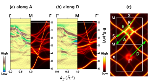
A very good agreement is found between ARPES and calculation in both the dispersive feature and the energy positions of the bands below eV. However, some discrepancies are also observed. Some of the calculated bands are missing in ARPES. In particular, the -crossing bands near and M in theory, originating from Te(1) -states, are not observed clearly in ARPES. Only the dim features are barely seen in Fig. 4(a) and (b). In order to see the bands near more clearly, the ARPES intensity plots in the vicinity of are shown in Fig. 5. Figures 5(a), (b), and (c) show the near- raw ARPES spectra of CeTe1.95Sb0.05 along E and those of CeTe2 along A and D in the BZ, respectively. Figure 5(d) shows the stack of momentum distribution curves (MDC’s), corresponding to the constant-energy cuts through the ARPES intensity plots shown in Fig. 5(c).
The band-crossing through is clearly observed in Fig. 5(a). These states are expected to produce the FS’s at the corresponding values.edc On the other hand, in Fig. 5(b) and (c), there are bands approaching , but their spectral intensities die away as they approach . The expected -crossing positions in ARPES agree very well with those in the calculated bands for the non-CDW phase of CeTe2 (see Fig. 4), which have mainly Te(1) character.Shim04 As shown in Fig. 4(c), two bands near () and M () in Fig. 5(b) would produce the inner (bright) FS and outer (dim) FS’s along -M in the first BZ, respectively. Similarly, the band near M () in Fig. 5(c) would produce the larger FS along -M in the second BZ. The much weaker spectral weight of the band near M in Fig. 5(b), as compared to that near , is attributed to its nature of the shadow band, which originates from the band-folding.
The vanishing spectral intensity near in Fig. 5 is considered to be related to the opening of the CDW gaps in some part of the FS’s. This feature is revealed more clearly in Fig. 5(f) and 5(g), which show the experimental FS maps of the first BZ and the second BZ, respectively, obtained by integrating meV. These are not the derivative data, but raw data. The inner FS near is certainly observed in Fig. 5(f), while the outer diamond FS is very weak. In contrast, the inner diamond FS near is hardly seen in Fig. 5(g) but the outer diamond FS is apparent. In view of the calculated FS’s in Fig. 4(c) and Fig. 5(e), such differences can be interpreted as the fact that the FS’s in Fig. 5(f) correspond to those in the first BZ, whereas the FS in Fig. 5(g) corresponds to that in the second BZ.
The feature of the vanishing spectral weight is also observed in some part of the FS’s: for example, in Fig. 5(f), the spectral weight near M is almost vanishing, and the outer diamond FS shows an intermittent feature. The polarization effect is not likely the origin of an intermittent feature of the outer FS since this feature is common for all four sides of the outer diamond. Instead, this region would correspond to the -points where CDW gaps open. Therefore the diminishing feature in Fig. 5(b) and (c) reflects the opening of the CDW gap. One can estimate the size of the CDW energy gap as being meV near M, in agreement with our previous finding in a different ARPES study.Kang06
In conclusion, the FS measured by ARPES agrees very well with the calculated FS for the undistorted CeTe2 both in shapes and sizes, and the -crossing metallic states are clearly observed in ARPES. We have found the following answers to the questions addressed in the beginning: (i) The measured FS is similar to that of LaTe2, implying that Ce states have a minor contribution to the CDW formation in CeTe2. (ii) The band-folding originating from the interaction with Ce-Te(2) layers produces the shadow bands and the corresponding FS’s, which have very weak spectral weight. (iii) The CDW modulation vector is estimated to be X.
This work was supported by the NRF under Contract No. 2009-0064246 and No. 2009-0079947. YSK acknowledges the NRF grant under Contract No. 2006-2002165 and 2009-0078025. PLS is supported by POSTECH and MEST in Korea.
References
- (1) J. Voit, et al., Science 290, 501 (2000).
- (2) T. Kasuya, M. H. Jung, and T. Takabatake, J. Magn. Magn. Mater. 220, 235 (2000).
- (3) T. Yokoya, et al., Science 294, 2518 (2001).
- (4) M. H. Jung, et al., Phys. Rev. B 67, 212504 (2003).
- (5) J.-S. Kang, et al., Phys. Rev. B 74, 085115 (2006).
- (6) J. K. Burdett and S. Lee, J. Amer. Chem. Soc. 105, 1079 (1983).
- (7) J.-S. Kang, et al., J. Phys.: Condens. Matter 16, 9163 (2004).
- (8) A. Kikuchi, J. Phys. Soc. Jpn. 67, 1308 (1998).
- (9) E. DiMasi, et al., Phys. Rev. B 54, 13587 (1996).
- (10) J. H. Shim, J.-S. Kang, and B. I. Min, Phys. Rev. Lett. 93, 156406 (2004).
- (11) K. Stöwe, J. Alloy Compd. 307, 101 (2000).
- (12) K. Y. Shin, et al., Phys. Rev. B 72, 085132 (2005).
- (13) D. R. Garcia, et al., Phys. Rev. Lett. 98, 166403 (2007).
- (14) T. Ito, et al., J. Magn. Magn. Mater. 310, 431 (2007).
- (15) We have employed the FLAPW band method in the LSDA++SO scheme. H. J. F. Jansen, A. J. Freeman, Phys. Rev. B 30, 561 (1984); P. Blaha et al., WIEN2k (ISBN 3-9501031-1-1), Karlheinz Schwarz, Techn. Universitat Wien, Austria (2001).
- (16) B. H. Min, H. Y. Choi, and Y. S. Kwon, Physica B 312-313, 203 (2002); ibid 312-313, 205 (2002).
- (17) The ground state and the electronic structures of CeTe2 remain almost the same in CeTe1.95Sb0.05 in this energy scale since the Sb-concentration in CeTe1.95Sb0.05 is very low ().
- (18) The map with = eV can be regarded as the FS because 0 is included in this map.
- (19) M. Lavagnini, et al., Phys. Rev. B 75, 205133 (2007).
- (20) K. E. Lee, et al., Phys. Rev. B 78, 134408 (2008).
- (21) QUANTUM ESPRESSO code, Giannozzi, et al., J. Phys. Condens. Matter 21, 395502 (2009).
- (22) All the cleaved surfaces were mirror-shiny, but had many stepped planes. Due to a finite acceptance angle of the electron analyzer and a different topography of a cleaved surface, each cleaved surface is expected to have a different yield.
- (23) W. Ku, T. Berlijn, C.-C. Lee, Phys. Rev. Lett. 104, 216401 (2010).
- (24) In the energy distribution curves (EDC’s), the photoemission peaks that cross were not observed clearly. Nevertheless, the -crossing of these bands is supported by the slope of these bands.