Further author information: (Send correspondence to T.K.) T.K.: E-mail: kitaguti@srl.caltech.edu
Spectral calibration and modeling of
the NuSTAR CdZnTe pixel detectors
Abstract
The Nuclear Spectroscopic Telescope Array (NuSTAR) will be the first space mission to focus in the hard X-ray ( keV) band. The NuSTAR instrument carries two co-aligned grazing incidence hard X-ray telescopes. Each NuSTAR focal plane consists of four 2 mm CdZnTe hybrid pixel detectors, each with an active collecting area of 2 cm 2 cm. Each hybrid consists of a array of 605 m pixels, read out with the Caltech custom low-noise NuCIT ASIC. In order to characterize the spectral response of each pixel to the degree required to meet the science calibration requirements, we have developed a model based on Geant4 together with the Shockley-Ramo theorem customized to the NuSTAR hybrid design. This model combines a Monte Carlo of the X-ray interactions with subsequent charge transport within the detector. The combination of this model and calibration data taken using radioactive sources of 57Co, 155Eu and 241Am enables us to determine electron and hole mobility-lifetime products for each pixel, and to compare actual to ideal performance expected for defect-free material.
keywords:
X-ray, -ray, CdZnTe, pixel detector, Monte-Carlo simulation1 Introduction
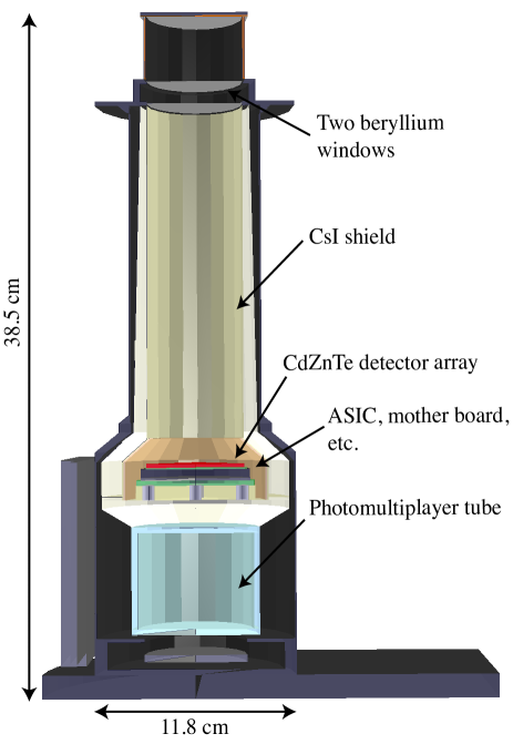
The Nuclear Spectroscopic Telescope Array (NuSTAR) mission[1] is a NASA Small Explorer that will carry the first focusing hard X-ray ( keV) telescopes to orbit. It is scheduled to be launched into low Earth orbit (550 km altitude, 6 deg inclination) by a Pegasus XL rocket from Kwajalein Atoll in February 2012. NuSTAR has two co-aligned telescopes, each consisting of a depth-graded multilayer optic[2, 3] focusing onto a cadmium zinc telluride (CdZnTe) pixel detector[4]. The detector is placed at the bottom of a cylindrical active CsI anti-coincidence shield to reduce detector background.
Cadmium zinc telluride (CdZnTe) and cadmium telluride (CdTe) semiconductor materials are attractive for use in astronomical hard X-ray instruments because, compared to alkali-halide scintillators, they can achieve superior spectral resolution and imaging detectors can be implemented in compact geometries. These materials also have relatively high atomic number (48 for Cd and 52 for Te) and a wide enough band gap ( eV) to permit near room temperature operation. Because of these advantages, cosmic hard X-ray detectors using CdZnTe and CdTe are already operating in space onboard the Swift[5] and INTEGRAL[6] satellites, respectively. Both missions contain coded aperture instruments with a large number of single planar detectors (32,768 CdZnTe for Swift, 16,384 CdTe for INTEGRAL). Due to the planar architecture, and the resulting relatively high capacitance and leakage current, and charge collection non-uniformity, the spectral resolution of these coded mask imagers is limited. NuSTAR will be the first astronomical mission to utilize CdZnTe hybrid pixel detectors, where the detector anode is divided into small segments, and low electronic noise, small leakage and good spectral resolution (1 keV FWHM from keV) is achievable.
Exploiting the good energy resolution for spectroscopy of astrophysical sources requires constructing a highly-accurate response model. For both CdZnTe and CdTe, the low hole mobility leads to a non-gaussian energy response, in particular spectral ’tailing’. As a result, determining the resolution kernel requires a detailed charge transport model, combined with Monte Carlo simulations. In addition, in the case of CdZnTe, current high-pressure Bridgman material growth processes produce crystals with a nonuniform distribution of charge transport properties. This results in variation of the charge transport properties across a centimeter-scale detector. We must therefore measure these properties for each pixel in order to construct a NuSTAR detector response model that can meet requirements for spectral reconstruction.
In this paper, we describe the NuSTAR spectral calibration program, the charge transport model, and we present results obtained by fitting data from NuSTAR flight detectors.
2 Cadmium-Zinc-Telluride Pixel Detector for NuSTAR
Each NuSTAR focal plane consists of four CdZnTe hybrid pixel detectors arranged in a array (see Figure 4 in [1]). The sensor element in each hybrid is a CdZnTe crystal with a segmented anode. Each anode pixel is attached to the input pad of a custom readout circuit using a gold-wire/conductive epoxy interconnect. The low-noise ASIC (NuCIT [7]), was developed by Caltech originally for the HEFT balloon program[8], and upgraded for homeland security and again for NuSTAR. The CdZnTe crystals were manufactured by Endicott Interconnects (formerly eV Products). Each crystal has an active collecting area of 2 cm 2 cm and a thickness of 2 mm. The cathode electrode is a monolithic platinum contact and the anode electrode is patterned into a grid with each pixel having pitch of 605 m, forming 1024 pixels for each hybrid. The pixel contacts are separated by a 50 m gap. The NuCIT ASIC contains a common on-chip analog-to-digital converter and an external microprocessor supports the readout. Each of the 1024 (a 32 x 32 array matched in pitch to the sensor) readout circuits has its own preamplifier, shaping amplifier, discriminator, sample and hold circuitry and test pulsar.
The NuCIT ASIC preamplifier and readout are designed so that both an electron signal and a hole signal can be determined for each event, allowing a depth of interaction measurement. To obtain pulse height information, the output of each pixel’s preamplifier is presented as a current signal sequentially and continuously to a bank of 16 sampling capacitors, with a ns (programmable) dwell time on each capacitor. The signal is also presented as a voltage to a discriminator. When a trigger occurs, sampling is halted. At this point the capacitor bank contains approximately eight samples “pre-trigger” and eight “post-trigger”. The integrated charge signal is obtained by subtracting the pre-trigger samples from the post-trigger samples. In normal operation, the instrument control processor searches all triggered pixels for the highest pulse height and reads nine sets of sixteen pulse height samples from a array. The processor packs the charge signal, obtained by performing the subtraction described above, into an array containing the pixel with the highest signal at the center, and the 8 surrounding pixels. In subsequent ground processing, based on a threshold determined in software, the surrounding pixels are sorted into electron (positive amplitude) and hole (negative amplitude) signals, and each group is summed. The negative amplitude hole signal results from the trapped holes creating image charge on the anode pixels (the holes are trapped for a timescale longer than the readout time). In order to cancel common mode noise, the average of the hole signal is subtracted from the electron signal.
Figure 2 shows a typical CdZnTe spectrum obtained with a 57Co radioactive source. The spectrum contains events where only the central pixel is triggered (ie. excluding events where charge is shared among multiple pixels). The energy resolution at 14.4 and 122 keV is 0.5 and 0.9 keV FWHM respectively. This resolution is much better than that achieved with a monolithic CdZnTe detector (7 keV at 122 keV for Swift[9], 9 keV at 100 keV for INTEGRAL[6]) due to the small pixel effect[10] and the ability to remove pixel-to-pixel charge collection variation. The test pulse, which appears at about 147 keV in the spectrum, has a width of 0.4 keV FWHM, showing the NuCIT ASIC and leakage current noise is very low. A low-energy tail associated with the 122 keV main peak is also seen in Figure 2. The tail structure is produced by a combination of hole trapping and Compton down-scattering of the line -rays in the radioactive source holder and passive material surrounding the detector.
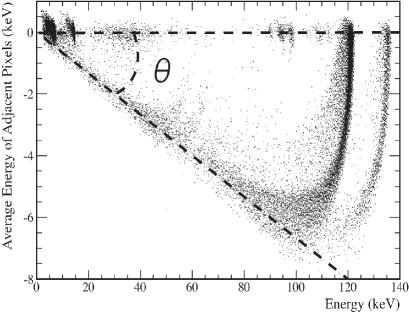
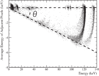
Figure 2 shows a scatter plot of the center pixel energy (electron signal) vs the average energy of the 8 surrounding pixels (hole image signal) for single pixel events. The events produced by 122 keV gamma-rays are largely distributed in a line tilted at an angle relative to the y-axis. At large values of hole signal, the event track curves back towards the origin. The location of an event on this track depends on interaction depth and the charge transport properties of the pixel. The central pixel pulse height decreases with interaction depth as a result of the variation in the magnitude of the image charge signal with depth. The closer to the anode the event occurs, the greater the image charge, and this image charge is both detected on the surrounding pixels, and subtracts from the central pulse height. Low-energy photons ( keV) interact only in a shallow region near the cathode surface and are observed to produce very little hole signal. However, the 122 keV photons in Figure 2 occur at a range of depths in the CdZnTe, and so produce the “depth curve”. When collapsed onto the X-axis to produce a standard spectrum, this is observed as a low-energy tail to the line.
An advantage of the depth measurement is that the CdZnTe activation background induced by cosmic radiation can be suppressed by flagging and rejecting events with large interaction depths. As noted above, photons with energy keV that enter through the aperture interact on average near the cathode surface, while the activation background occurs uniformly in the CdZnTe crystal. We can then flag and reject events that occur deep in the detector as background events.
 |
 |
3 Monte-Carlo Simulator
3.1 Overview of Simulator
It is almost impossible to analytically calculate the detector response of CdZnTe pixel detectors because the geometry of the focal plane detector is complex, and moreover the physical processes governing particle interactions have many channels and branches. Monte-Carlo simulations provide the only method of calculating the spectral response function. In order to generate the pixel-by-pixel response, we have developed a Monte-Carlo simulator based on the Geant4 toolkit[11] together with a charge transport model customized to the NuSTAR hybrid design described in §2. The NuSTAR focal plane geometry in Figure 4 has been described with Geomega, one of the MEGAlib[12, 13] software libraries designed for medium-energy -ray astronomy.
The simulator is operated on an object-oriented software framework called ANL[14], originally developed for the ASCA satellite in the 1990s, and improved for the follow-on Suzaku and ASTRO-H missions. The ANL framework is based on the concept that a complicated process can be decomposed into many simple modules, and can be described as a chain of them. Each ANL module includes an initial function, a function for event-by-event analysis, and a termination function. The ANL framework calls these modules in the order defined by the chain. The Geant4 run manager and three user mandatory classes (the primary particle generator, detector geometry constructor, and physics process manager) are wrapped into the corresponding ANL modules separately. Examples of the successful application of this combination of Geant4 and ANL framework can be seen in the generation of the detector response for the hard X-ray detector onboard Suzaku[15] and the background estimation for the soft -ray detector onboard ASTRO-H[16].
 |
 |
3.2 Charge Transport Model
The Geant4 Monte Carlo engine generates hit information such as times, positions, and deposited energies for each physical interaction. After collecting the hit information, the downstream ANL modules calculate the output charge induced on each anode pixel, and convert them into digitized values by considering the response of the sensor and the properties of the electronics. The electron and hole charge transport is the most important among the processes because the low-energy tails are generated by charge (in particular hole) trapping. We have therefore paid special attention to developing an accurate and complete charge transport model.
In the first stage of the model, we calculate the fraction of charge shared among anode pixels using the deposited energy and interaction position. We assume that the electron cloud can be described by a 2-d Gaussian shape on the plane parallel to the electrode, with a standard deviation, , which increases as a function of time. The electron cloud spreads due to two physical processes; random thermal motion of electrons, and electron-electron repulsion. According to Benoit and Hamel (2009) [17], the diffusion equation describing charge cloud spreading due to thermal motion and repulsive force is given by
| (1) |
where is the electron mobility, is the Boltzmann constant, is the operating temperature, is the elementary charge, is the number of electron-hole pairs as a function of the deposited energy, and are the vacuum permittivity and the relative permittivity of CdZnTe (typically 10.9), respectively. The first and second terms on the right hand side represent diffusion effects due to thermal motion and repulsion force, respectively. The standard deviation at the moment electrons arrive at the anode pixel can be obtained by solving equation (1) using the Runge-Kutta method, assuming that the initial value of the standard deviation is set to 1 m for every energy deposition. As show in in Figure 4, the electron cloud size is quite dependent on the repulsive force – without including electrostatic repulsion the electron cloud size is underestimated by %. The fraction of charge collected on each pixel is determined by integrating the normalized 2-d Gaussian area with the obtained standard deviation in the corresponding anode pixel region. This charge sharing model predicts about 2/3 of events have only one triggered pixel (single-pixel event) and the rest have multiple triggered pixels. The ratio is in good agreement with observed results.
Next we determine the charge induction efficiency of each pixel. The Shockley-Ramo theorem (eg. [18]) provides a convenient way to calculate induced charge due to the motion of charge carriers. The charge induction efficiency at any time, , is given by
| (2) |
where is the position at time, , is the interaction position where electron-hole pairs are generated, is the charge carrier mobility-lifetime product, is the applied electric field, and and are the weighting potential and weighting field. The e and h subscripts represent electrons and holes. The first and second terms on the right hand side represent the charge induction efficiency for electrons and holes, respectively. The exponential terms describes carrier trapping effects. This treatment does not consider detrapping, since that occurs on a timescale longer than the electronics response time. In the case of an ideal single CdZnTe detector, which has a uniform applied electric field and a uniform weighting field throughout the detector volume, equation (2) becomes the well-known Hecht relation[19].
We require a fine-mesh to describe the weighting potential in order to numerically integrate equation (2). Because some electrons drift toward the adjacent pixels due to diffusion, the weighting potential requires a pixel array consisting of the center and 8 adjacent pixels. We divide the detector volume containing pixels into 31 million rectangular cells consisting of parts on a side and 240 parts in depth. The weighting potential at each cell center is calculated by using the approximate solution[20] assuming the cathode electrode is an infinite plane. We assume an anode pitch of 605 m and a detector thickness of 2 mm provide the boundary values for the calculation. Each pixel is assumed to have an identical weighting potential even if it is near the crystal edge.
We require calculation of the carrier track in order to calculate equation (2). To be exact, each charge carrier drifts along a different path due to random thermal motion. However, it would require long computation times to individually integrate equation (2) for every single path. In order to shorten the computing time, we assume that all holes take the shortest path from interaction point to the cathode electrode. These holes are drifted in the vertical (cathode) direction with a constant velocity given by the hole mobility multiplied by the applied electric field, presumed to be constant throughout the CdZnTe volume. Electrons also take the shortest path from the interaction point to individual anode pixels, which have a significant amount of shared charge. In this work, this amount is set to be more than 0.1%, determined by our charge sharing model. The charge induction efficiency the anode of each pixel is estimated by numerically integrating equation (2), using the shortest charge carrier path.
We obtain the charge sharing ratio and the charge induction efficiency of individual anode pixels for each physical interaction as described above. In the final stage, we calculate the energy deposition in each pixel by multiplying the deposited energy by the ratio and efficiency. We then calculate the total energy of each pixel by summing up all of the energies produced by every physical interactions in the CdZnTe detector. Because the observed energy is broadened due to Poisson fluctuations in the number of hole-electron pairs, and the variation in paths traveled by the charge carriers, the final energy deposition is randomly smoothed by a Gaussian. Using these energies, we can reproduce the CdZnTe spectrum in Figure 2 and the scatter plot in Figure 2.
4 Measurement of Charge Transport Properties
To reproduce the spectral response of each pixel, the NuSTAR Monte Carlo simulator needs a determination of the electron and hole mobility-lifetime products, assigned by equation (2), for each pixel. We determine these charge transport properties by using calibration data taken with radioactive sources with a range of line energies spanning the NuSTAR band. The calibration data are fit using comparison data produced by the NuSTAR Monte Carlo simulator as described below.
In order to determine the mobility-lifetime product for electrons, we take data to determine the voltage dependence of a peak channel (total charge signal), , given approximately by
| (3) |
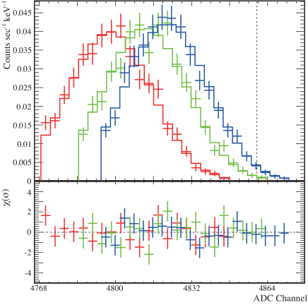
where is the peak channel with no electron trapping, is the detector thickness (2 mm for the NuSTAR CdZnTe detector), and is the applied high voltage. The electron trapping, described by the exponential term, becomes strong as the voltage decreases. Figure 6 shows an example of voltage scan spectra taking with 241Am at three different voltages compared to spectral models produced by the Monte-Carlo simulator. The spectral peak shifts to lower energy as a function of decreasing high voltage as expected, with the magnitude of the shift relatively well described by the model (). The derived is cm2 V-1. This method for measuring is the same as that for the Swift CdZnTe detectors [9], but the weighting potential is customized for to the NuSTAR hybrid design.
In order to establish a procedure for determining the hole mobility-lifetime product using the simulation code, we fit the energy vs. depth of interaction plot. Figure 6 shows energy vs. depth scatter plots for two different hole mobility-lifetime products. We found that -rays that interact subject to a particular mobility-lifetime produce a distribution with respect to the anode electrode with a definite angle, , shown in Figure 6. The absolute angle monotonically decreases as the hole mobility-lifetime products increases. We can therefore measure the mobility-lifetime products for holes by comparing the observed angle to a data base of angles database calculated by the simulator.
 |
 |
 |
For determining the electron mobility-lifetime product we used bias voltages of 300, 400 and 500 V and for each illuminated the detectors with a 241Am source placed about 3 inch above the center of the motherboard where the CdZnTe hybrids are installed. We operated the detectors at 5 ∘C at atmospheric pressure. Each data set at was taken at a constant voltage for 12 hours. For the hole mobility-lifetime products we obtained data with 57Co and 155Eu radioactive sources, illuminating the detectors for 24 hours for each source. We confirmed by simulating data that these measurement time periods are long enough to determine the mobility-lifetime products for electrons and holes within the required accuracy.
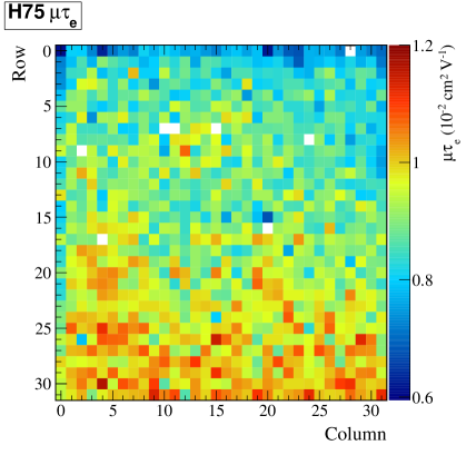
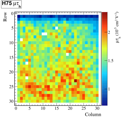
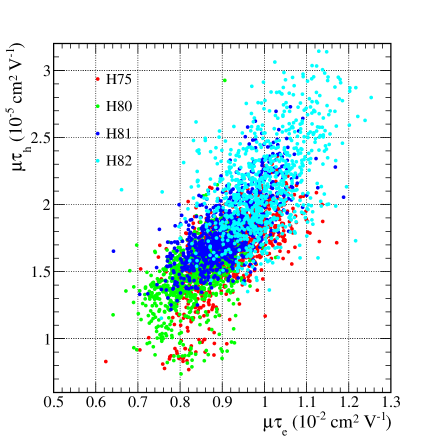
Figure 8 and 8 show pixel maps of mobility-lifetime products for electrons and holes, respectively, obtained by analyzing the calibration data sets. The mobility-life time product for electrons ranges from to cm2 V-1, while the mobility-lifetime product for holes ranges from to cm2 V-1. Typical errors are 3% and 5% in the 1 confidence level for the mobility-lifetime products for electrons and holes, respectively. The two spatial maps are similar in pattern. A correlation diagram of the mobility-lifetime products between electrons and holes for 4 different CdZnTe hybrids is shown in Figure 9. Although these 4 crystals were prepared from different CdZnTe ingots, the correction is modestly strong with a correlation coefficient of 0.72. The strong correlation is reasonable because crystal defects suggest mobility-lifetime products for electrons and holes should be related.
 |
 |
5 Evaluation of Spectral Model
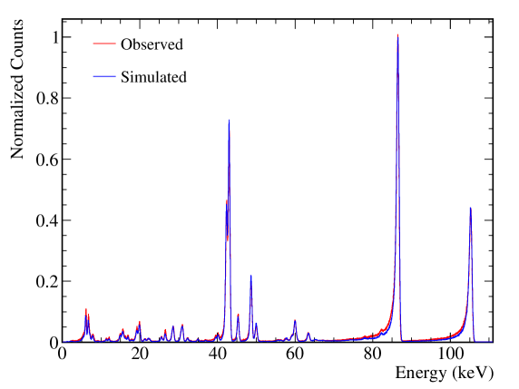
In order to evaluate the accuracy of the NuSTAR detector model with the measured charge transport properties, we obtained data during the instrument thermal vacuum test, when the detectors were at the expected in-flight operating temperature, by irradiating the calibrated CdZnTe hybrids with the flight 155Eu radioactive calibration source which is integrated into the focal plane assembly. The four hybrids were installed in the flight CsI shield. By turning on the CsI shield, signals produced by charged particles and -rays Compton-scattered with the shield can be eliminated using the anti-coincidence scheme. This event selection was incorporated into the model.
We performed a full Monte-Carlo simulation using the measured charge transport properties to generate a summed spectrum model for the entire CdZnTe pixel array. Figure 10 compares the simulation result to the real data. The model can reproduce the experimental data within about 10% accuracy, with the exception of the low-energy tail structures. This is acceptable at the pre-flight stage. The model for two peaks around 29 and 31 keV, which are fluorescence X-rays from the CsI shield excited by -rays from the 155Eu source, is also in good agreement with the observed one. This agreement demonstrates that the anti-coincidence model in the simulation is accurate. The disagreement of the tail components are possibly produced by an extra charge loss near the gap surface between anode pixels[21]. We need further studies to improve the model.
 |
6 Summary
We have developed a Monte-Carlo simulation code for the NuSTAR CdZnTe pixel detectors that generates a spectral model as a function of incident energy. By comparing simulated models to observed data, we succeed in extracting mobility-lifetime products for electrons and holes independently for all CdZnTe pixels. We found a correlation (r = 0.72) between the obtained mobility-lifetime products for electrons and holes as a function of pixel. The spectral response model we have developed for each individual pixel can accurately reproduce calibration data taken on the flight detectors in the laboratory.
Acknowledgements.
This work was supported under NASA Contract NNG08FD60C. T.K. is supported by JSPS postdoctoral fellowships for research abroad. We thank Csaba Szeles for useful discussions.References
- [1] Harrison, F. A., Boggs, S., Christensen, F., Craig, W., Hailey, C., Stern, D., Zhang, W., et al., “The Nuclear Spectroscopic Telescope Array (NuSTAR),” in [Society of Photo-Optical Instrumentation Engineers (SPIE) Conference Series ], Society of Photo-Optical Instrumentation Engineers (SPIE) Conference Series 7732 (July 2010).
- [2] Koglin, J. E., An, H., Blaedel, K. L., Brejnholt, N. F., Christensen, F. E., Craig, W. W., Decker, T. A., Hailey, C. J., Hale, L. C., Harrison, F. A., Jensen, C. P., Madsen, K. K., Mori, K., Pivovaroff, M. J., Tajiri, G., and Zhang, W. W., “NuSTAR hard x-ray optics design and performance,” in [Society of Photo-Optical Instrumentation Engineers (SPIE) Conference Series ], Presented at the Society of Photo-Optical Instrumentation Engineers (SPIE) Conference 7437 (Aug. 2009).
- [3] Hailey, C. J., An, H., Blaedel, K. L., Brejnholt, N. F., Christensen, F. E., Craig, W. W., Decker, T. A., Doll, M., Gum, J., Koglin, J. E., Jensen, C. P., Hale, L., Mori, K., Pivovaroff, M. J., Sharpe, M., Stern, M., Tajiri, G., and Zhang, W. W., “The Nuclear Spectroscopic Telescope Array (NuSTAR): optics overview and current status,” in [Society of Photo-Optical Instrumentation Engineers (SPIE) Conference Series ], Presented at the Society of Photo-Optical Instrumentation Engineers (SPIE) Conference 7732 (July 2010).
- [4] Rana, V. R., Cook, III, W. R., Harrison, F. A., Mao, P. H., and Miyasaka, H., “Development of focal plane detectors for the Nuclear Spectroscopic Telescope Array (NuSTAR) mission,” in [Society of Photo-Optical Instrumentation Engineers (SPIE) Conference Series ], Presented at the Society of Photo-Optical Instrumentation Engineers (SPIE) Conference 7435 (Aug. 2009).
- [5] Gehrels, N., Chincarini, G., Giommi, P., Mason, K. O., Nousek, J. A., Wells, A. A., White, N. E., et al., “The Swift Gamma-Ray Burst Mission,” ApJ 611, 1005–1020 (Aug. 2004).
- [6] Ubertini, P., Lebrun, F., Di Cocco, G., Bazzano, A., Bird, A. J., Broenstad, K., Goldwurm, A., La Rosa, G., Labanti, C., Laurent, P., Mirabel, I. F., Quadrini, E. M., Ramsey, B., Reglero, V., Sabau, L., Sacco, B., Staubert, R., Vigroux, L., Weisskopf, M. C., and Zdziarski, A. A., “IBIS: The Imager on-board INTEGRAL,” A&A 411, L131–L139 (Nov. 2003).
- [7] Cook, W. R., Burnham, J. A., and Harrison, F. A., “Low-noise custom VLSI for CdZnTe pixel detectors,” in [Society of Photo-Optical Instrumentation Engineers (SPIE) Conference Series ], O. H. Siegmund & M. A. Gummin, ed., Presented at the Society of Photo-Optical Instrumentation Engineers (SPIE) Conference 3445, 347–354 (Nov. 1998).
- [8] Harrison, F. A., Christensen, F. E., Craig, W., Hailey, C., Baumgartner, W., Chen, C. M. H., Chonko, J., Cook, W. R., Koglin, J., Madsen, K.-K., Pivavoroff, M., Boggs, S., and Smith, D., “Development of the HEFT and NuSTAR focusing telescopes,” Experimental Astronomy 20, 131–137 (Dec. 2005).
- [9] Sato, G., Parsons, A., Hullinger, D., Suzuki, M., Takahashi, T., Tashiro, M., Nakazawa, K., Okada, Y., Takahashi, H., Watanabe, S., Barthelmy, S., Cummings, J., Gehrels, N., Krimm, H., Markwardt, C., Tueller, J., Fenimore, E., and Palmer, D., “Development of a spectral model based on charge transport for the Swift/BAT 32K CdZnTe detector array,” Nuclear Instruments and Methods in Physics Research A 541, 372–384 (Apr. 2005).
- [10] Barrett, H. H., Eskin, J. D., and Barber, H. B., “Charge Transport in Arrays of Semiconductor Gamma-Ray Detectors,” Physical Review Letters 75, 156–159 (July 1995).
- [11] Geant4 Collaboration, Agostinelli, S., Allison, J., Amako, K., Apostolakis, J., Araujo, H., Arce, P., Asai, M., Axen, D., et al., “Geant4-a simulation toolkit,” Nuclear Instruments and Methods in Physics Research A 506, 250–303 (July 2003).
- [12] Zoglauer, A., Andritschke, R., and Schopper, F., “MEGAlib The Medium Energy Gamma-ray Astronomy Library,” New A Rev. 50, 629–632 (Oct. 2006).
- [13] Zoglauer, A., Andritschke, R., Boggs, S. E., Schopper, F., Weidenspointner, G., and Wunderer, C. B., “MEGAlib: simulation and data analysis for low-to-medium-energy gamma-ray telescopes,” in [Society of Photo-Optical Instrumentation Engineers (SPIE) Conference Series ], Presented at the Society of Photo-Optical Instrumentation Engineers (SPIE) Conference 7011 (Aug. 2008).
- [14] Ozaki, M., Watanabe, S., Terada, Y., Itoh, T., Kitsunezuka, M., Kishishita, T., Ishisaki, Y., and Takahashi, T., “Framework for a Geant4-Based Simulator of the Radiation Background and Detector Responses of the Space X-Ray Observatory Suzaku (Astro-E2),” IEEE Transactions on Nuclear Science 53, 1310–1316 (June 2006).
- [15] Terada, Y., Watanabe, S., Ohno, M., Suzuki, M., Itoh, T., Takahashi, I., Sato, G., Murashima, M., Kawano, N., Uchiyama, Y., Kubo, S., Takahashi, T., Tashiro, M., Kokubun, M., Makishima, K., Kamae, T., Murakami, T., Nomachi, M., Fukazawa, Y., Yamaoka, K., Nakazawa, K., and Yonetoku, D., “Development of a Monte Carlo Simulator for the Astro-E2 Hard X-Ray Detector (HXD-II),” IEEE Transactions on Nuclear Science 52, 902–909 (Aug. 2005).
- [16] Mizuno, T., Hiragi, K., Fukazawa, Y., Umeki, Y., Odaka, H., Watanabe, S., Kokubun, M., Takahashi, T., Nakajima, K., Nakazawa, K., Makishima, K., Nakahira, S., Terada, Y., and Tajima, H., “Monte Carlo simulation study of in-orbit background for the soft gamma-ray detector on-board ASTRO-H,” in [Society of Photo-Optical Instrumentation Engineers (SPIE) Conference Series ], Presented at the Society of Photo-Optical Instrumentation Engineers (SPIE) Conference 7732 (July 2010).
- [17] Benoit, M. and Hamel, L. A., “Simulation of charge collection processes in semiconductor CdZnTe -ray detectors,” Nuclear Instruments and Methods in Physics Research A 606, 508–516 (July 2009).
- [18] He, Z., “Review of the Shockley-Ramo theorem and its application in semiconductor gamma-ray detectors,” Nuclear Instruments and Methods in Physics Research A 463, 250–267 (May 2001).
- [19] Hecht, K., “Zum Mechanismus des lichtelektrischen Primärstromes in isolierenden Kristallen,” Zeitschrift fur Physik 77, 235–245 (Mar. 1932).
- [20] Kabir, M. Z. and Kasap, S. O., “Charge collection and absorption-limited x-ray sensitivity of pixellated x-ray detectors,” Journal of Vacuum Science Technology 22, 975–980 (May 2004).
- [21] Chen, C. M. H., Boggs, S. E., Bolotnikov, A. E., Cook, W. R., Harrison, F. A., and Schindler, S. M., “Numerical modeling of charge sharing in CdZnTe pixel detectors,” IEEE Transactions on Nuclear Science 49, 270–276 (Feb. 2002).