Size Dependence of Current–Voltage Properties
in Coulomb Blockade Networks
Abstract
We theoretically investigate the current–voltage (–) property of two-dimensional Coulomb blockade (CB) arrays by conducting Monte Carlo simulations. The – property can be divided into three regions and we report the dependence of the aspect ratio (namely, the lateral size over the longitudinal one ). We show that the average CB threshold obeys a power-law decay as a function of . Its exponent corresponds to a sensitivity of the threshold depending on , and is inversely proportional to (i.e., at fixed ). Further, the power-law exponent , characterizing the nonlinearity of the – property in the intermediate region, logarithmically increases as increases. Our simulations describe the experimental result obtained by Parthasarathy et al. [Phys. Rev. Lett. 87 (2001) 186807]. In addition, the asymptotic – property of one-dimensional arrays obtained by Bascones et al. [Phys. Rev. B. 77 (2008) 245422] is applied to two-dimensional arrays. The asymptotic equation converges to the Ohm’s law at the large voltage limit, and the combined tunneling-resistance is inversely proportional to . The extended asymptotic equation with the first-order perturbation well describes the experimental result obtained by Kurdak et al. [Phys. Rev. B 57 (1998) R6842]. Based on our asymptotic equation, we can estimate physical values that it is hard to obtain experimentally.
1 Introduction
A Coulomb blockade (CB) [1, 2] emerges in condensed matter physics, and it causes threshold and nonlinear current–voltage (–) behavior. In some sense, CB can be regarded as a phenomenon that occurs in disordered systems with thresholds such as charge-density waves [3] and Wigner crystals [4]. CB was first studied in a single–electron transistor [1, 5]. Nowadays, it is studied in many systems such as arrays of metallic islands [6, 7, 8], metal nanocrystal arrays [9, 10, 11], molecular arrays [12, 13, 14, 15], a Tomonaga–Luttinger liquid such as a carbon nanotube [16, 17, 18], and graphene quantum-dot arrays [19]. Some numerical studies of CB have been done, e.g. Monte Carlo (MC) methods [20, 21, 22, 23, 24], molecular dynamics (MD) simulations [25, 26, 27], and circuit dynamics [28, 29]. In most of these cases, a core work is to investigate its – property. It is known that the – property of typical CB arrays can be divided into three characteristic regions according to path flow of electrons [10, 25]: near the CB threshold , the intermediate voltage region, and the large voltage region. Several static trajectories exist near the threshold, and a crossover from a static to a dynamic trajectory occurs when the bias voltage is set in the intermediate region [25]. As the bias voltage increases, trajectories are again static and linear. The – property thus approaches to Ohmic behavior in the large voltage region.
The – property near the CB threshold is mainly characterized by the value of the CB threshold. The threshold is determined by trajectory of electrons, and is thus sensitive to conditions such as the array size and surface disorder. The – property is approximately described as
| (1) |
where is the bias voltage. In the intermediate region, the – property also exhibits nonlinear behavior described as eq. (1). The value of for several systems has been determined from both experiments and simulations. For example, an experimental study shows that an array of normal metal islands has for a one-dimensional (1D) array and for a two-dimensional (2D) square array [7]; in addition, other experimental studies show that a metal nanocrystal has for a 2D triangle array [10], and that a gold nanocrystal has to for a 3D array [11]. Experiments of colloidal deposition show for 2D and for 3D [30]. For numerical simulations, MC calculations show that for linear arrays and for square arrays [21], and MD calculations show that for square arrays [25]. In a theoretical study, a mean-field analysis suggested that for a 2D array [31]. By analyzing surface evolution on arrays with charge disorder, is analytically predicted [21]. Here, we should emphasize that has been discussed in relation to the array configuration and array dimension so far; the size dependence has not been taken into account. Meanwhile, some previous studies [30, 9, 25] mention that the exponent monotonically increases with increasing the lateral size from a 1D linear array to a 2D square array. However, they have qualitatively focused on only the arrays in which the lateral size is less than the longitudinal one and expected the exponent to be constant for large lateral size.
Middleton and Wingreen (MW) explicitly introduced offset charge distribution in their model. The charge disorder originates from the surface impurity. In their model, Bascones et al. have discussed the asymptotic – property of 1D arrays in the large voltage region [23]. It converges to the Ohm’s law at the large voltage limit. In addition, they showed the presence of the offset voltage , and analytically expressed it in short-limit of the interaction range.
In this paper, we carry out MC simulations to study the size dependence of the – property for configurations such as a simple lattice and a triangular lattice. We employ the model proposed by MW [21]. Based on their model, we extend it to size dependence. Our main results are the following: (i) the average CB threshold , (ii) the power-law exponent in the intermediate voltage region, and (iii) an asymptotic – curve of 2D arrays with the first-order perturbation of .
This paper is organized as follows. In § 2, we briefly describe the present configurations, simulation model, and numerical conditions. In § 3, we first express the size dependence of the average CB threshold for simple configurations, and then, the size dependences of the exponent is shown for several configurations. In addition, we express the asymptotic – property obtained analytically for simple configurations, and then we compare it with simulation and experimental results to verify the asymptotic relation. In § 4, we summarize our results.
2 Method
2.1 Structure
The simplest single-electron transistor consists of two tunnel junctions that connect the source and drain electrode, respectively, and the region sandwiched between the tunnel junctions also connects to the gate electrode through the gate capacitor. The sandwiched region, known as the Coulomb island, can be regarded as a place where charge accumulates. We consider arrays constructed of Coulomb islands between positive and negative electrodes. A series of tunneling processes cause electrons to flow in the arrays. Each island also connects to the gate electrode with the gate capacitor. The i-th island has charge and potential . The charge contains both an integer multiple of the elementally charge (where denotes an integer and the elementary charge) and offset charge due to the impurity [21]. In simulations, the offset charges are set by uniform random numbers and remain constant over time.
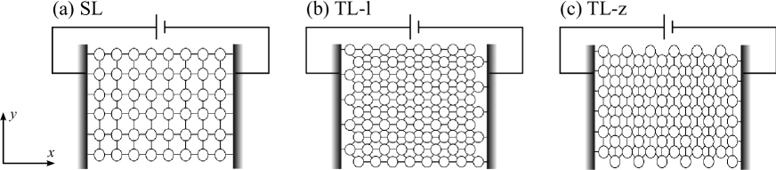
Three configurations are considered (Fig. 1). The first configuration is a simple lattice (SL), and the remaining two configurations involve different directions of a triangular lattice: a line-type triangular lattice (TL-l) and a zigzag-type triangular lattice (TL-z). We set - and -directions as shown in Fig. 1, namely -direction corresponds to longitudinal direction and -direction does to lateral one. The SL configuration is characterized by the number of horizontal islands and vertical islands . Thus, the total number of islands is . Both the TL-l and TL-z configurations are also characterized by and , and the total number of islands is . Although we use and in every configurations, the method of setting them is underspecified for triangular lattices. Here, we define and as described in the caption of Fig. 1, and the aspect ratio is defined as the lateral size over the longitudinal size; i.e., .
To calculate the total energy of the array, it is useful to consider a configuration matrix. The physical configuration of the lattices uniquely determines the configuration matrix whose element is represented as
| (2) |
where denotes the tunneling capacitance between the i-th and j-th islands, the tunneling capacitance between the i-th island and the electrode , and the Kronecker delta. Note that the symbols , , and indicate the positive, negative, and gate electrodes, respectively. If the i-th island does not connect to the j-th one, then is set to 0. Electrons move through the network of islands, while the islands themselves do not move. Therefore, the configuration matrix remains constant over time in this study.
2.2 Model
We briefly summarize the time-evolution procedure used in the MC method [20, 21] in this subsection.
The system evolves to decrease the total electrostatic energy , whose derivation is summarized in Appendix A. In MC simulations, the electrons are virtually moved for each possible tunneling event. We can calculate the energy change at (see Appendix B), where . The tunneling rate at is calculated as [32]
| (3) |
where denotes the tunneling resistance at . It is assumed that the tunnel resistance between an island and the gate electrode is infinity in these calculations, i.e., the electrons cannot move between an island and the gate electrode. The tunneling rate is derived by assuming that the tunneling events occur independently. The resistances depend on the configuration of the array in general, but we regard them to be a constant , where .
Assuming Poisson distribution, the probability distribution that a tunneling from to occurs at time lag is represented as
| (4) |
Then, the cumulative distribution is equivalent to the distribution that a tunneling from to occurs during time lag , represented as
| (5) |
where denotes the time when the last tunneling event from to occurred. The energy changes depend on time, and hence the tunneling rate also does. A uniform random number in is introduced and the cumulative distribution is set as . Note that the random number is updated only when a tunneling event from to occurs. We thus obtain the time interval between the last tunneling event from to and the next one as
| (6) |
where denotes the number of tunneling events within the entire array during . Note that remains constant over time , and is not equal to in general. We use the smallest for the time evolution increments.
2.3 Simulation
Below the CB threshold , the tunneling interval is infinity for each path. Therefore, we can determine the threshold voltage above which is finite in the steady state. The current along the path can be calculated as
| (7) |
In simulations, the current can be calculated along all path, but we focus only on those paths that neighbor the positive or negative electrodes, represented as
| (8) |
where the sigma with the prime denotes summation over only those islands that neighbor the positive or negative electrodes. In the steady state, and are the same because of Kirchhoff’s current law. Hence, we demonstrate only as the current in the remaining sections.
The voltages of the negative and gate electrodes are fixed at , and the voltage of the positive electrode is thus adjusted as the control parameter, i.e., the bias voltage is equivalent to the voltage of the positive electrode . The initial condition was and . The voltage was incremented by , and before we sampled the physical variables at each voltage, we waited sufficiently long for the system to return to the steady state. Note that this waiting time depends on system conditions, such as the configuration and .
We assume that the system is at zero temperature. The capacitance is set at , Note that the ratio corresponds to the interaction range[21]. The increment voltage is ; therefore the threshold voltage has an uncertainty of the order . Finally, the charge is scaled by , the capacitance by , the time by , the current by , the potential by , and the energy by .
3 Results and Discussion
3.1 Size dependences of the average threshold
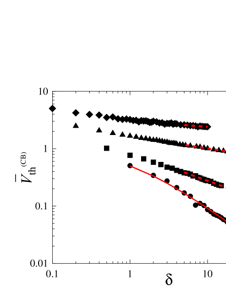
We first investigate the size dependences of the average CB threshold for SL. Figure 2 shows the average CB threshold as a function of the aspect ratio for several longitudinal size . Each point on the figure is derived from the average of at least 50 different initial distributions of the offset charges. Our results of 1D arrays (i.e., ) are in agreement with the previous results by MW [21].
The average threshold is analytically represented as
| (9) |
For the simplest case and , the CB threshold voltage as a function of the initial charge is obtained as
| (10) |
namely, of a single Coulomb island is proportional to the initial offset charge. For (i.e., ) and , the threshold is dominated by the smallest initial offset charge. The average threshold reduces to
| (11) | |||||
| (13) |
where denote the reordered dimensionless charges: . The average threshold for is thus obtained as
| (15) |
and this well describes the simulation result as shown in Fig. 2. For , it is difficult to derive the average threshold because electron meandering plays an important role just above . Nevertheless, we find that the average CB threshold for large can be described by a power law
| (16) |
In fact, eq. (15) for large implies the power-law decay as eq. (16).
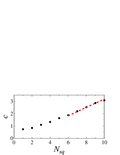
The proportionality coefficient of eq. (16) indicates the value of the average threshold for square arrays (i.e., ). Figure 3 shows the coefficient as a function of that is a length of a side of square arrays. MW have reported for square arrays [21], and the line is plotted in Fig. 3. The simulation results deviate from the line in small region. This is because we cannot regard the array with as a square array, namely, is too small to regard arrays as square in that region. In addition, the simulation results do not satisfy the power law near at small .
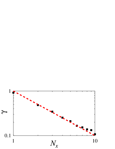
The power-law exponent of eq. (16) is shown in Fig. 4. The relation for is evident from eq. (15). The exponent is thus interpreted as a sensitivity of the threshold depending on comparing to arrays with . As increases, the increment of the aspect ratio decreases even for the same increment of . Therefore, it can be expected that is a monotonically decreasing function of . In fact, as shown in Fig. 4, the exponent is inversely proportional to , namely,
| (17) |
These results will be a hint to understand the size dependences of the CB threshold. In addition, it is interesting to observe the power law decay in experiments.
3.2 Logarithmic increase of the power-law exponent
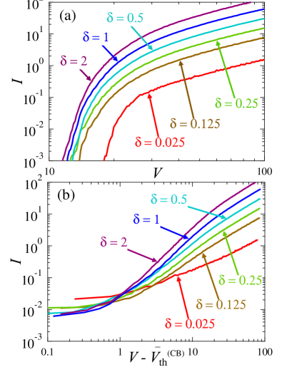
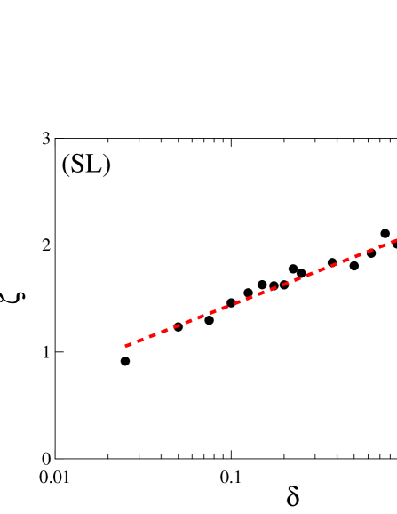
We next investigate the exponent in eq. (1) as a function of the aspect ratio . Figure 5 shows the averaged – property for several , and each curve results from the average of at least 30 data sets. The nonlinear behavior is more visible in Fig. 5 (b). Further, Fig. 6 shows the exponent as a function of with . The exponents are obtained by fitting to the average – property in the intermediate region defined as . The fitting range is selected to prevent artificiality from being included into the value of the exponents. The aspect ratio dependence of appears to be approximately represented by
| (18) |
with fitting parameters and . The parameter denotes the exponent of the square array, and approximately agrees with the previous result [21]. Using the parameter, the exponent for a 1D simple array, i.e., , is represented as
| (19) |
and is obtained as shown in Fig. 6. MW have reported that, for arbitrary , the exponents of linear and square arrays are and , respectively [21]. The same logarithmic increase is thus expected to appear in different longitudinal size (i.e., ), while we only show single longitudinal size (i.e., ) in Fig. 6. Moreover, although our simulations are only performed for finite in each configuration, it is expected that the exponent diverges logarithmically at such large values of .
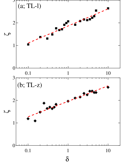
We also focus on the triangular lattices. Figures 7 (a) and (b) show the exponent as a function of the aspect ratio for TL-l and TL-z, respectively. Note that, similar to SL, the – properties are averaged over at least 30 data sets and the exponent is extracted from the averaged results. Here, the intermediate region is defined as , and the fitting is done in that range. Similar to the exponent of SL, the exponents of TL-l and TL-z increase logarithmically as determined by eqs. (18) and (19). Parthasarathy et al. [10] experimentally showed for a well-ordered triangular array of gold nanocrystals with an array size of to and . In the range , our simulation results of both TL-l and TL-z show . Our results propose that we should pay attention to the aspect ratio as well as the array configuration and array dimension when discussing the exponent .
We should recall that the universality of the logarithmic increase requires careful attention. The above results are obtained in locally coupled CB, i.e., small . The behavior of for large may differ from that for small , because the interaction among electrons ranges over the entire array in large systems. The dependences are still an open question.
3.3 Analytical asymptotic equation at large bias voltages
We finally discuss the – property for large values of the bias voltage . As mentioned above, Bascones et al. have derived the asymptotic – property of 1D arrays with the offset voltage Their offset voltage is expressed in the limit of [23]. We extend their study to 2D simple configurations. In addition, our extended expression of contains the first-order perturbation of .
Figure 8 shows the – plot for several sizes of the SL configuration. All results exhibit linear behavior at large bias voltage limit, and the asymptotic curve can be obtained as follows. The energy changes of the 1D array that contains islands reduce to (see Appendix B)
| (20a) | |||||
| (20c) | |||||
| (20d) | |||||
with n . At large bias voltages, the current from the negative to the positive electrode is neglected. Thus, the all energy changes should be always the same in the large voltage region. We can obtain as
| (21) |
Here, the above representation contains an offset voltage defined as
| (22) |
The offset voltage differs from the CB threshold . For , can be analytically derived within the first-order perturbation of (see Appendix C) as
| (23) |
The energy changes cannot be the same below the offset voltage . In contrast, above the offset voltage , electrons can move from the negative to positive electrode for any offset charge distributions, i.e., is the maximum of when [33]. However, near , the influence of the offset charge distribution cannot be neglected because the charge of electrons is discrete. With increasing the bias voltage, the energy changes become sufficiently large to neglect this discreteness. Therefore, all energy changes in the large voltage region can be always regarded as the same.
Using eq. (7), the asymptotic current is obtained as
| (24) |
Note that it is independent of the gate voltage. The simple array can be easily extended to higher-dimensional arrays. For the 2D array in which the number of islands is , the lateral current (i.e., the -direction current in Fig. 1) can be neglected at large bias voltages. This 2D array can be assumed to be composed of the isolated 1D arrays that consist of islands. Hence, we obtain
| (25) | |||||
| (26) |
The above equation does not hold when , because the assumption that the current from the negative to positive electrode is negligible is no longer correct at these high temperatures. In contrast, in finite temperature, eq. (LABEL:IVrelation_asy_2D) represents that the asymptotic equation converges in the limit of to the Ohmic behavior with the combined tunneling-resistance
| (28) |
Namely, the combined tunneling-resistance is inversely proportional to the aspect ratio ; at large .
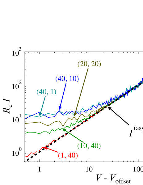
As shown in Fig. 9, which plots as function of , the asymptotic line calculated from eq. (LABEL:IVrelation_asy_2D) completely describes simulation results of arbitrary at large bias voltages (roughly, ). Near the offset voltage , the simulation results deviate from the asymptotic line because each energy change is different from the others. As mentioned above, this originates from discreteness of charge. In fact, as decreases (i.e., the number of the energy changes decreases), the results collapse to the asymptotic line at smaller .
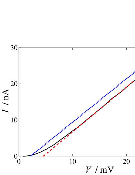
We next compare the asymptotic result with the experimental result [8] measured by Kurdak et al. Because the physical parameters are known, this experimental result is suitable for testing the asymptotic equation. Figure 10 shows the experimental (sample A in reference [8]) and the asymptotic results for the following experimental conditions from reference [8]: (i.e., ), fF, fF, k, and mK. The temperature is sufficiently small for neglecting the exponential dependence in eq. (LABEL:IVrelation_asy_2D), and we neglect the square of . The asymptotic results typically describes the experimental result, as shown in Fig. 10. The asymptotic fitting parameters lead to k and fF. The resistance is in good agreement with the value in reference [8]. On the other hand, the capacitance evaluated from the asymptotic equation is smaller than that estimated by Kurdak et al. Several reasons can be considered. First, our expression of neglects higher terms of and one might consider the higher-term effects. Second, the capacitance ratio is sensitive to . As shown in Fig. 10, the order of obtained from fitting is different from that estimated by Kurdak et al., while the difference of is 2.4 mV. In addition, it is difficult to experimentally evaluate the value of in general. In fact, Kurdak et al. stated ”our knowledge of is less precise,” and they estimated the value of from the specific capacitance. Instead, the asymptotic equation may allow us to approximately evaluate the configuration of the array and some physical variables (, , , and ) in experiments from observations of the offset voltage and the asymptotical slope at large voltages.
4 Summary
We conducted MC simulations to investigate the – properties of CB arrays. To understand the – property, our strategy was dividing it into three regions characterized by the path flow of electrons, and we pay attention to the size (i.e., aspect ratio ) dependence. Our main results were (i) power-law behavior of the average CB threshold , (ii) the power-law exponent in the intermediate voltage region, and (iii) an asymptotic – curve at large voltages.
We derived an analytical relationship [eq. (15)] for the average CB threshold for , and we found that the average CB threshold obeys a power-law decay as a function of the aspect ratio . The coefficient is in agreement with the previous study by MW [21]. In addition, its power-law exponent is inversely proportional to the longitudinal size (i.e., at fixed ) [eq. (17)]. It is difficult to obtain the analytical form for because trajectories of electrons meander. Nevertheless, our analytical and simulation results provide a hint for further development of the study.
The size dependences of the exponent were shown for different array configurations such as SL, TL-l, and TL-z. The exponent in arrays of large was considered to be constant so far. However, we revealed that logarithmically increases as increases for both the simple and triangular lattices. Namely, in addition to the array configuration and array dimension, the aspect ratio is a significant variable for discussing the exponent .
We extended the asymptotic equation for 1D arrays without interaction [23] to 2D arrays with first-order perturbation of the interaction range [eq. (LABEL:IVrelation_asy_2D) with eq. (23)]. At sufficient large voltages, the equation adequately describes the Ohmic behavior and the combined tunneling-resistance is inversely proportional to . The offset voltage , included in the asymptotic equation, differs from the CB threshold . Instead, the offset voltage can be regarded as the maximum of the in the limit of [33]. These asymptotic property well agrees with simulation and experimental results. Our extended equation allows to estimate physical values and array configuration which are experimentally hard to obtain. The asymptotic equations for other configurations are also expected to show similar results and to converges to the Ohm’s law. The details will be discussed elsewhere.
We thank Profs. Takuya Matsumoto, Megumi Akai, and Takuji Ogawa at Osaka University for fruitful discussions. This work was partially supported by the MEXT, a Grant-in-Aid for Scientific Research on Innovative Areas ”Emergence in Chemistry” (Grant No. 20111003) and another Grant-in-Aid for Scientific Research (Grant No. 21340110).
Appendix A Total Energy
The charge of the i-th island is represented by
| (29) |
Assuming that the capacitances are nonzero only between neighboring island–island and island–electrode pairs, eq. (29) reduces to
| (30) |
where denotes the matrix of capacitances defined by eq. (2). The capacitance should be zero by definition. Equation (2) thus indicates that the diagonal elements are the sum of all capacitances associated with an island, and the off-diagonal elements (ij) are the negative of the capacitance between the i-th and the j-th islands. The potential is formally solved to obtain
| (31) |
where denotes the potential corresponding to the electrodes defined by
| (32) |
The total electrostatic energy of the system is equivalent to the sum of the work for storing charge under potential in each island and the energy of the electrodes, represented as,
| (33) |
where the last term denotes the energy of the electrodes and the charge at the electrodes . Note that the interparticle electrostatic energy must not be double-counted.
Appendix B Energy Change
Let us consider the tunneling of an electron whose charge is from the n-th to m-th island. The energy change is
| (34) |
where and denote the energy changes with respect to the first and second terms of eq. (33), respectively. The charge changes to with the tunneling; therefore,
| (35) | |||||
| (38) | |||||
| (40) | |||||
| (41) |
where the trivial relationship is used and the effective potential is introduced as
| (42) |
Similarly,
| (43) | |||||
| (44) |
Next, let us consider the tunneling from the n-th island to an electrode . Similar to the above discussion, the energy change is represented as
| (45) |
Given that the charge change is , the energy change is obtained as
| (47) | |||||
| (48) |
and
| (49) |
In addition, the following equations hold:
| (50) | |||||
| (51) | |||||
| (52) |
Appendix C Offset Voltage
The configuration matrix for a 1D simple array is represented as
| (53) |
with arbitrary . The inverse elements () and () are derived as
| (54) | |||||
| (55) |
where denotes the determinant of the configuration matrix for the 1D simple array that contains islands and . The offset voltage reduces to
| (56) |
Note that the above representation holds for arbitrary .
References
- [1] T. A. Fulton and G. J. Dolan: Phys. Rev. Lett. 59 (1987) 109.
- [2] T. Heinzel: Mesoscopic electronics in solid state nanostructures (Wiley-VCH, Weinheim, 2003).
- [3] G. Grüner: Rev. Mod. Phys. 60 (1988) 1129.
- [4] F. I. B. Williams, P. A. Wright, R. G. Clark, E. Y. Andrei, G. Deville, D. C. Glattli, O. Probst, B. Etienne, C. Dorin, C. T. Foxon, and J. J. Harris: Phys. Rev. Lett. 66 (1991) 3285.
- [5] D. V. Averin and K. K. Likharev: in Single Electronics: Correlated Transfer of Single Electron and Cooper Pairs in Systems of Small Tunnel Junctions, ed. B. L. Altshuler, P. A. Lee, and R. A. Webb (Elsevier, Amsterdam, 1991), p. 173.
- [6] J. E. Mooij, B. J. van Wees, L. J. Geerligs, M. Peters, R. Fazio, and G. Schön: Phys. Rev. Lett. 65 (1990) 645.
- [7] A. J. Rimberg, T. R. Ho, and J. Clarke: Phys. Rev. Lett. 74 (1995) 4714.
- [8] C. Kurdak, A. J. Rimberg, T. R. Ho, and J. Clarke: Phys. Rev. B 57 (1998) R6842.
- [9] C. T. Black, C. B. Mrray, R. L. Sandstrom, and S. Sun: Science 290 (2000) 1131.
- [10] R. Parthasarathy, X.-M. Lin, and H. M. Jaeger: Phys. Rev. Lett. 87 (2001) 186807.
- [11] H. Fan, K. Yang, D. M. Boye, M. K. J. Sigmon Thomas, H. Xu, G. P. Lopez, and C. J. Bringker: Science 304 (2004) 567.
- [12] M. A. Reed, C. Zhou, C. J. Muller, T. P. Burgin, and J. M. Tour: Science 278 (1997) 252.
- [13] W. Schoonveld, J. Wildeman, D. Fichou, P. Bobbert, B. J. van Wees, and T. Klapwijk: Nature 404 (2000) 977.
- [14] J. Kane, M. Inan, and R. F. Saraf: ACS nano 4 (2010) 317.
- [15] K. Stokbro: J. Phys. Chem. C 114 (2010) 20461.
- [16] M. Bockrath, D. Cobden, J. Lu, A. Rinzler, R. Smalley, L. Balents, and P. McEuen: Nature 397 (1999) 598.
- [17] Z. Yao, H. Postma, L. Balents, and C. Dekker: Nature 402 (1999) 273.
- [18] M. Monteverde, M. Núñez Regueiro, G. Garbarino, C. Acha, X. Jing, L. Lu, Z. W. Pan, S. S. Xie, J. Souletie, and R. Egger: Phys. Rev. Lett. 97 (2006) 176401.
- [19] D. Joung, L. Zhai, and S. I. Khondaker: Phys. Rev. B 83 (2011) 115323.
- [20] U. Geigenmuller and G. Schon: Europhys. Lett. 10 (1989) 765.
- [21] A. A. Middleton and N. S. Wingreen: Phys. Rev. Lett. 71 (1993) 3198.
- [22] M. Suvakov and B. Tadic: Computational Science - ICCS 2007, Pt 2, Proceedings, Vol. 4488, 2007, p. 641.
- [23] E. Bascones, V. Estévez, J. A. Trinidad, and A. H. MacDonald: Phys. Rev. B 77 (2008) 245422.
- [24] M. Suvakov and B. Tadic: J. Phys.: Cond. Matter 22 (2010) 163201.
- [25] C. Reichhardt and C. J. Olson Reichhardt: Phys. Rev. Lett. 90 (2003) 46802.
- [26] J. Tekić, O. M. Braun, and B. Hu: Phys. Rev. E 71 (2005) 026104.
- [27] C. Reichhardt and C. J. Olson Reichhardt: Phys. Rev. Lett. 96 (2006) 028301.
- [28] T. Oya, I. N. Motoike, and T. Asai: Int. J. Bifurcat. Chaos 17 (2007) 3651.
- [29] A. K. Kikombo, T. Oya, T. Asai, and Y. Amemiya: Int. J. Bifurcat. Chaos 17 (2007) 3613.
- [30] C. Lebreton, C. Vieu, A. Pépin, and M. Mejias: Micro. Eng. 42 (1998) 507.
- [31] S. Roux and H. J. Herrmann: Europhys. Lett. 4 (1987) 1227.
- [32] K. K. Likharev: Dynamics of Josephson Junctions and Circuits (Gordon and Breach Publishers, 1986).
- [33] T. Narumi, M. Suzuki, Y. Hidaka, T. Asai, and S. Kai: submitted to Phys. Rev. Lett.