Magnetic and Electronic Properties of Metal-Atom Adsorbed Graphene
Abstract
We systematically investigate the magnetic and electronic properties of graphene adsorbed with diluted 3-transition and noble metal atoms using first principles calculation methods. We find that most transition metal atoms (i.e. Sc, Ti, V, Mn, Fe) favor the hollow adsorption site, and the interaction between magnetic adatoms and -orbital of graphene induces sizable exchange field and Rashba spin-orbit coupling, which together open a nontrivial bulk gap near the Dirac points leading to the quantum-anomalous Hall effect. We also find that the noble metal atoms (i.e. Cu, Ag, Au) prefer the top adsorption site, and the dominant inequality of the AB sublattice potential opens another kind of nontrivial bulk gap exhibiting the quantum-valley Hall effect.
pacs:
73.22.Pr, 75.50.Pp, 75.70.TjIntroduction —. After an initial rush RMPgraphene since its first experimental exfoliation Geim2004 , graphene research has turned toward the application of graphene-based electronics RMPgraphene ; GraApplication . Graphene itself is a zero-gap semiconductor characterized by the linear Dirac-type dispersion, which is closely related to many amazing properties, e.g. high electron mobility and half-integer quantum Hall effect (per spin and valley). However, a band gap in graphene is highly desirable for designing semiconductor devices. So far, there are several proposals of engineering a band gap, such as by employing a staggered AB sublattice potential DiXiao , strain effect strain , intrinsic spin-orbit coupling Kane in single layer graphene, or applying a perpendicular electric field in bilayer graphene BilayerGap .
Graphene is also considered as a promising candidate for spintronics, which generally require imbalanced spin up and down carrier populations. However, the pristine graphene is nonmagnetic, and one need to employ external methods to magnetize it, e.g. by decorating hydrogen, sulfur or metal adatoms on graphene MagnetizedHSF ; Cohen ; Savini , or substituting metal impurities for carbon atoms in graphene substitution . Alternatively, spin-orbit coupling is thought to be another source for manipulating the spin degrees of freedom through electric means SO-spintronics . In graphene there are two kinds of spin-orbit couplings: intrinsic and extrinsic Kane . The former one has been shown to be unrealistically weak WeakSOI . The latter one, which is also known as Rashba spin-orbit coupling, arises from the top-bottom layer symmetry breaking due to the presence of a substrate or strong perpendicular electric field, which was reported to be remarkably large in graphene placed on top of Ni(111) surface Rashba .
| supercell | supercell | ||||||||||
|---|---|---|---|---|---|---|---|---|---|---|---|
| Atoms | site | E | site | E | |||||||
| Sc | H | 1.92 | 1.26 | 2.5 | 0.97 | H | 1.97 | 1.43 | 2.5 | 0.89 | 2.30 |
| Ti | H | 1.86 | 1.76 | 0.0∗ | 0.88 | H | 1.86 | 1.75 | 1.4 | 0.87 | 3.41 |
| V | H | 1.89 | 0.94 | 0.0∗ | 0.67 | H | 1.87 | 1.01 | 2.2 | 0.71 | 4.51 |
| Cr | B(H) | 2.33(2.17) | 0.14(0.13) | 0.0() | 0.35(0.41) | B(H) | 2.37(2.15) | 0.16(0.15) | 0.0∗(2.5) | 0.37(0.45) | 5.64(5.52) |
| Mn | H | 2.07 | 0.14 | 4.5 | 0.56 | H | 2.09 | 0.14 | 4.5 | 0.57 | 5.42 |
| Fe | H | 1.56 | 0.98 | 0.81 | H | 1.56 | 0.95 | 5.5 | 0.81 | 1.97 | |
| Co | H | 1.55 | 1.31 | 0.0∗ | 0.63 | H | 1.53 | 1.67 | 0.0∗ | 0.66 | 0.99 |
| Ni | H | 1.58 | 1.37 | 60 | 0.51 | H | 1.58 | 1.39 | 0.0 | 0.52 | 0.00 |
| Cu | T(H) | 2.24(2.17) | 0.24(0.10) | 0.7(0.4) | 0.16(0.14) | T(H) | 2.25(2.17) | 0.25(0.10) | 38.8(7.0) | 0.15(0.15) | 0.90(0.92) |
| Zn | H | 3.78 | 0.03 | 0.6 | 0.02 | H | 3.78 | 0.02 | 0.0 | 0.02 | 0.00 |
| (LDA) | H | 3.04 | 0.14 | 13.9 | 0.03 | H | 3.02 | 0.14 | 0.0 | 0.03 | 0.00 |
| Au | T(H) | 3.13(3.47) | 0.14(0.13) | 0.0∗(2.9) | -0.08(-0.09) | T(H) | 3.45(3.54) | 0.16(0.16) | 0.6(1.7) | -0.02(-0.15) | 0.84(0.84) |
| (LDA) | T(H) | 2.37(2.43) | 1.20(0.94) | 9.4(2.0) | -0.06(-0.05) | T(H) | 2.40(2.52) | 0.77(0.50) | 161.4(8.6) | -0.09(-0.09) | 1.03(0.96) |
| Ag | T(H) | 3.57(3.69) | 0.03(0.03) | 0.0(1.5) | 0.04(0.02) | T(H) | 3.49(3.58) | 0.03(0.03) | 3.0(2.3) | 0.02(0.02) | 1.00(1.00) |
| (LDA) | T(H) | 2.45(2.52) | 0.82(0.76) | 2.8(6.8) | 0.08(0.07) | T(H) | 2.44(2.51) | 0.38(0.31) | 21.8(8.7) | 0.11(0.08) | 0.87(0.93) |
In this Letter, we present a systematic investigation on the magnetic and electronic properties of graphene adsorbed with 3-transition and noble metal atoms including the spin-orbit coupling using first principles calculation methods. The results show that most transition metal adatoms favor the hollow site, while the noble metal adatoms prefer the top site. We find that both types of adsorption give rise to nontrivial bulk gaps. Further Berry-phase analysis NiuRMP demonstrates that the gap opening mechanisms are completely distinct, i.e. one arises from the joint effect of exchange field and Rashba spin-orbit coupling leading to the quantum-anomalous Hall (QAH) effect, while the other one originates from the inequality of the AB sublattice potential resulting in the quantum-valley Hall (QVH) effect. Our findings should not only provide a new scheme for the gap opening in graphene, but also show great potential for the realization of the long-sought quantum anomalous Hall effect and the dissipationless valleytronics.
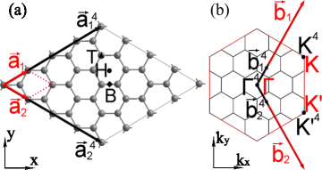
Computational Methods —. The adatom-graphene system is modeled using one metal atom on top of a (=3, 4) supercell of graphene. As illustrated in Fig. 1(a), a supercell is composed of carbon atoms and one metal atom, and the single atom has three possible adsorption sites: hollow (H), top (T), and bridge (B). Panel (b) plots the Brillouin-zone of the supercell comparing to that of the supercell with well-defined valley indices and .
The first principles calculations were performed using the projected-augmented-wave method PAW as implemented in the Vienna Ab-initio Simulation Package (VASP) VASP . The generalized gradient approximation (GGA) exchange-correlation functional GGA was mainly used except those specified by the local density approximation (LDA) in Table 1. The kinetic energy cutoff was set to be 500 eV, and the experimental lattice constant of graphene was used. During the structure relaxation, all atoms were allowed to relax along the normal direction of graphene and all parameters were chosen to converge the forces to less than 0.01 . The first Brillouin-zone integration was carried out by using the and Monkhorst-Pack grids for the and supercells, respectively. A vacuum buffer space of 15 Å was set to prevent the interaction between adjacent slabs.
Adsorption Analysis —. Table 1 summarizes the stable adsorption sites, energetic and structural properties of 12 kind of 3-transition and noble metal atoms for the and supercells. The stable adsorption site, distance and magnetization of adatoms were obtained by only considering the magnetization, while other quantities were calculated by further including the spin-orbit coupling. The adsorption energy is defined as: , where , and are the energies of the isolated atom, supercell of graphene, and adatom- supercell of graphene, respectively. The charge transfer was calculated based on the Bader charge analysis chargeTransfer . For clear demonstration, we divide the adsorption analysis into two parts:
(a) For the 3-transition metal adatoms, we observe that most of them except Cr favor the hollow site. (i) For Sc, Ti, V, Fe, Co, and Ni, the adsorption distances are very short (less than ), and the adsorption energy and the charge transfer are very large, which together indicate a strong hybridization; (ii) For Cr and Mn, the adsorption distance is slightly larger than , the adsorption energy is relatively weak but the charge transfer is still remarkably large, which corresponds to a moderately weak adsorption; (iii) For Zn, both the large adsorption distance and extremely small adsorption energy and charge transfer signal an extremely weak hybridization. In the following, we show that the reconstruction of the electronic configurations of the adsorbed metal atoms is intimately dependent on the strength of adsorption on the graphene sheet.
In Table 1, we notice that the magnetic moments of adatoms are greatly altered compared to that of the isolated atoms. This is found to obey the following rules: (1) When the 3-shell is less than half filled (i.e. Sc, Ti, V), the strong hybridization lowers the energy of the 3-orbital. This makes the 4 electrons transfer to the unoccupied 3-orbital. Since the resulting 3-shell is not over half-filled, the Hund’s rule dictates that all the 3 electrons possess the same spin-polarization leading to the increase of the magnetic moments ; (2) When the 3-shell is exactly half-filled (i.e. Cr, Mn), the adsorption is weak therefore the 3-orbital energy is less affected during the hybridization. Based on the Hund’s rule, all 3-electrons are equally spin-polarized showing a maximum magnetization. In the influence of the high magnetization from the 3-shell, the 4 electrons tend to align with the spin of the 3 electrons, which slightly increases the magnetic moment; (3) When the 3-shell is over half-filled (i.e. Fe, Co, Ni), the strong hybridization lowers the 3-shell energy and the transfer of 4 electrons to 3-orbital decreases the magnetic moment due to the occupying of the unpaired 3-orbital Cohen . In particular, for Ni the two 4 electrons are transferred to -orbital and form a closed 3 shell, giving rise to a vanishing magnetic moment; (4) For atoms with closed 3 and 4 shells (i.e. Zn), it behaves like a inert atom leaving graphene nearly unaffected.
(b) For the noble metal adatoms, we find that they are stable at the top adsorption site. Consistent with Ref. [Cohen, ], the long adsorption distance, low adsorption energy, and weak charge transfer originate from the physical adsorption involving the van de Waals forces. In Table 1, we also provide the LDA results for Au and Ag adsorption. The major differences are that the adsorption distance is dramatically decreased and the adsorption energy is exponentially increased. Because of the closed shells, the single valence electron contributes to the magnetic moment .
Due to the magnetic proximity effect with the magnetic adatoms, graphene can be magnetized. In the absence of spin-orbit coupling, we estimated the induced exchange field exchangefield near the Dirac points to be =145 (Sc), 277 (Ti), 199 (V), 359 (Cr), 181 (Mn), 57 (Fe), 462 (Co), 0 (Ni), 51 (Cu) in units of meV for the hollow-site adsorption on the supercell.
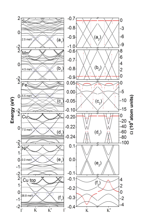
Band Structures and Berry Curvatures—. We classify the twelve atoms into three groups: (1) atoms (e.g. Sc, Mn, Fe) adsorbed at the hollow site, and graphene is magnetized; (2) atoms (e.g. Ni) adsorbed at the hollow site, but graphene is not magnetized; (3) atoms (e.g. Cu) adsorbed at the top site. To capture the physics arising from the Dirac points, we center on the adsorption on the supercells. The adsorption on the supercells will be discussed in the supplementary materials.
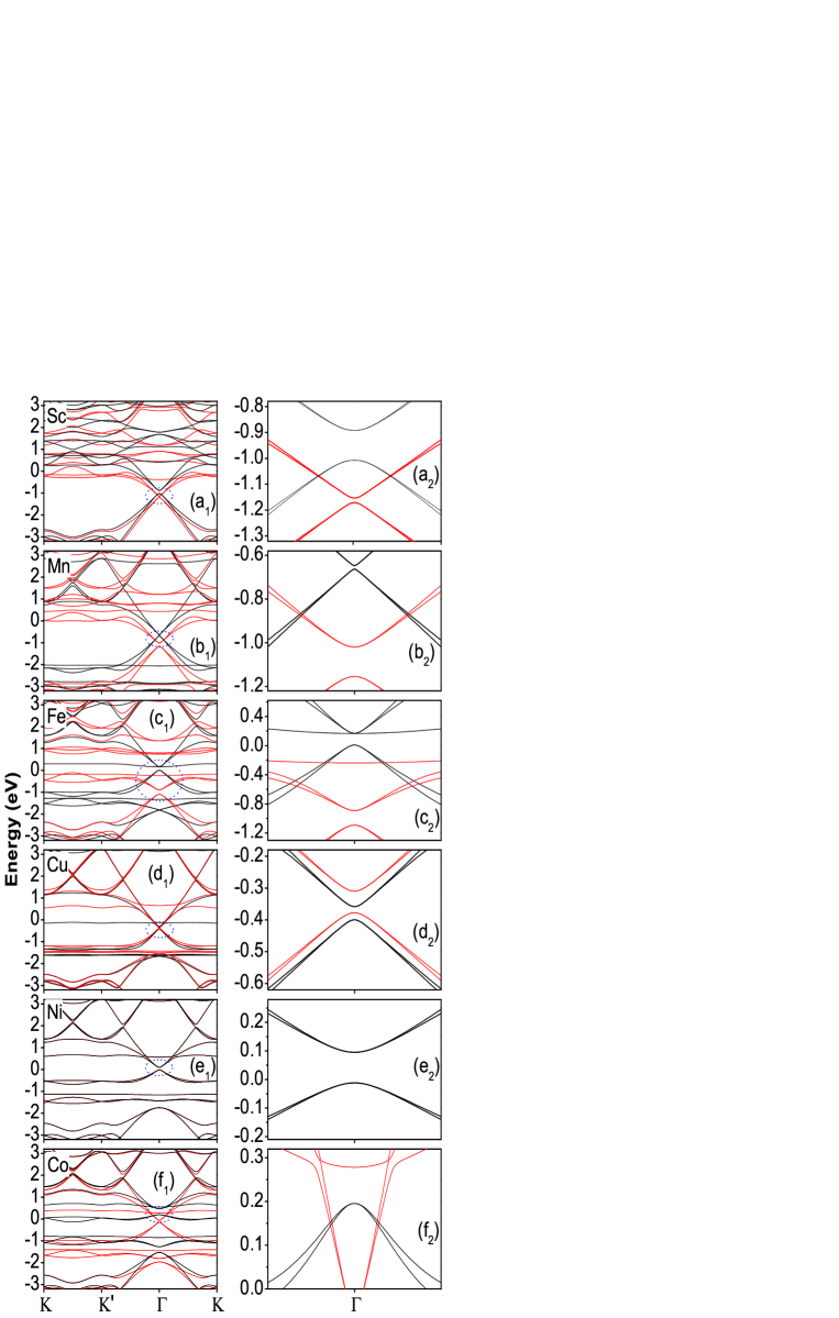
Figure 2 plots the band structures of adatom-graphene for (a) Sc, (b) Mn, (c) Fe, (d) Cu, (e) Ni adsorbed at the hollow sites and (f) Cu adsorbed at the top site. Panels ()-() exhibit the full bulk bands along the high symmetry lines, and panels ()-() zoom in the bands near the Dirac points and . We see that sizable bulk band gaps open at the Dirac points in panels ()-() and (). The presence of such a bulk gap indicates an insulating state. However, we note that all the Fermi levels lie outside the bulk gaps except that in panel () for Fe-adsorption. Thus, to realize this insulator one has to artificially adjust (e.g. by applying a gate voltage) the Fermi levels to be inside the gap.
To further identify the nontrivial topological properties of the obtained insulators, we turn to the Berry phase analysis in the momentum space NiuRMP . By constructing the Bloch wavefunctions from self-consistent potentials, the Berry curvature can be obtained using the following formula Kubo1 ; Kubo2 ; Kubo3 :
| (1) |
where the summation is over all bands below the bulk band gap, is the Fermi-Dirac distribution function, , and is the velocity operator. In panels ()-() and (), we also plot the Berry curvatures in dotted curves. One can observe that in panels ()-() the Berry curvatures at point share the same sign as that at point. By integrating the Berry curvatures over the first Brillouin zone, it gives rise to a nonzero Chern number for the insulating state of Sc, Fe, Cu adsorption, and for the insulating state of the Mn adsorption. The non-vanishing Chern number in the absence of magnetic field signifies a QAH state Supp , which was proposed theoretically haldane but still not realized in experiment. In the subsequent section, we show the mechanism of the formation of the QAH effect in graphene.
Figure 2 clearly shows that the adatoms of group (i) can open a non-trivial bulk band gap and achieve the QAH effect, but that of group (ii) can not. Therefore, we conclude that the magnetization in graphene, which breaks the time-reversal symmetry, is an essential ingredient for the QAH effect. Alternatively, we find that no bulk band gap opens for the group (i) atom-adsorption when the spin-orbit coupling is switched off. This makes the spin-orbit coupling the other key ingredient of the QAH effect. From Table 1, one can notice that there is substantial charge transfer from the metal adatoms to graphene. Due to the asymmetry of the adatom-graphene structure, a sizable potential gradient is formed at the interface, which induces a considerable Rashba spin-orbit coupling Rashba . Panel () for Cu adsorbed at the hollow site further supports that the 4 spin-polarized electron transfer can also realize the QAH state. Therefore we summarize that the realization of the QAH state is only dependent on the spin-polarized charge transfer, but independent of the details in the adsorption (i.e. strong/weak hybridization). Although the induced Rashba spin-orbit coupling and magnetization in graphene are non-uniformly distributed in the structure, the gap opening mechanism near the Dirac points is similar to that of the tight-binding model with uniformly distributed Rashba spin-orbit coupling and magnetization qiao : first, the magnetization lifts the spin up and down bands, accompanying with the bands crossing; second, the Rashba spin-orbit coupling opens a bulk gap at the bands crossing points.
Because of the Van de Vaals force, the noble metal adatoms favor the top adsorption site. Besides the resulting Rashba spin-orbit coupling and exchange field, the major difference from the hollow-site adsorption is the extra introduction of the inequality of AB-sublattice potential, which breaks the spacial inversion symmetry. For example, we have considered the case with Cu adsorbed at the top site as shown in the panel (). Through plotting the Berry curvature distribution, we observe that at point exhibits opposites sign as that at point. This strongly signals a QVH state with canceling Chern numbers Supp , i.e. , but . We can attribute this result to the leading role of the AB sublattice inequality suppressing the joint effect from Rashba spin-orbit coupling and exchange field.
Conclusions —. We study the magnetic and electronic properties of graphene adsorbed with 12 metal atoms using first principles calculation methods. We show that the QAH effect can be realized by doping the magnetic adatoms (i.e. Sc, Ti, V, Mn, Fe, Cu, Ag, and Au) at the hollow site of graphene, which originates from the joint effect between the Rashba spin-orbit coupling and magnetization. We also find that when the noble metal atoms (i.e. Cu, Ag, and Au) are adsorbed at the top site, the QVH effect can be observed due to the inversion symmetry breaking from the inequality of the AB sublattice potential. Our findings of the QAH and QVH states in the adatom-graphene systems not only provides a new gap opening scheme for the industrial application, but also pave the way for the realization of the dissipationless charge/valley current in spintronics and valleytronics.
Acknowledgement —. Z.Q. was supported by NSF (DMR 0906025) and Welch Foundation (F-1255). Q.N. was supported by DOE (DE-FG03-02ER45958, Division of Materials Science and Engineering) and Texas Advanced Research Program. Y.Y. was supported by NSF of China (10974231) and the MOST Project of China (2007CB925000, and 2011CBA00100). The Texas Advanced Computing Center and Supercomputing Center of Chinese Academy of Sciences are gratefully acknowledged for high performance computing assistance.
† These authors contribute equally;
‡ ygyao@aphy.iphy.ac.cn;
§ On leave from the University of Texas at Austin.
References
- (1) W. J. Beenakker, Rev. Mod. Phys. 80, 1337 (2008); A. H. Castro Neto et al., Rev. Mod. Phys. 81, 109162 (2009).
- (2) K. S. Novoselov et al., Science 306, 666 (2004).
- (3) F. Chen et al., Nano Lett. 9, 2571 2009; Y. Zheng et al., Phys. Rev. Lett. 105, 166602 (2010).
- (4) D. Xiao et al., Phys. Rev. Lett. 99, 236809 (2007); S. Y. Zhou el al., Nature Mat. 6, 770 (2009).
- (5) F. Guinea et al., Nat. Phy. 6, 30 (2010).
- (6) C. L. Kane, and E. J. Mele, Phys. Rev. Lett. 95, 146802 (2005).
- (7) J. B. Oostinga et al., Nat. Mat. 7, 151 (2008); Y. Zhang el al.,Nature 459, 820 (2009).
- (8) Y. G. Zhou et al., J. Appl. Phys. 105, 104311 (2009); J. Zhou et al., Appl. Phys. Lett. 95, 103108 (2009); J. Zhou et al., Nano Lett. 9, 3867 (2009).
- (9) K. T. Chan et al., Phys. Rev. B 77, 235430 (2008).
- (10) G. Savini et al., Phys. Rev. Lett. 105, 037002 (2010).
- (11) E. J. G. Santos et al., Phys. Rev. B 81, 125433 (2010).
- (12) I. Zutic et al., Rev. Mod. Phys. 76, 323 (2004); D. Awschalom et al., Physics 2, 50 (2009).
- (13) Y. G. Yao et al., Phys. Rev. B 75, 041401(R) (2007); H. Min et al., Phys. Rev. B 74, 165310 (2006).
- (14) A. Varykhalov et al., Phys. Rev. Lett. 101, 157601 (2008); Y. S. Dedkov et al., Phys. Rev. Lett. 100, 107602 (2008).
- (15) It is obtained from at point.
- (16) D. Xiao, M.-C. Chang, and Q. Niu, Rev. Mod. Phys. 82, 1959 (2010).
- (17) P. E. Blöchl, Phys. Rev. B 50, 17953 (1994).
- (18) G. Kresse et al., Phys. Rev. B 54, 11169 (1996).
- (19) J. P. Perdew et al., Phys. Rev. B 46, 6671 (1992).
- (20) W. Tang et al., J. Phys.: Condens. Matter 21, 084204 (2009).
- (21) D. J. Thouless et al., Phys. Rev. Lett. 49, 405 (1982).
- (22) M. C. Chang, and Q. Niu, Phys. Rev. B 53, 7010 (1996).
- (23) Y. G. Yao et al., Phys. Rev. Lett. 92, 037204 (2004).
- (24) See the Supplementary Materials for details.
- (25) F. D. M. Haldane, Phys. Rev. Lett. 61, 2015 (1988); C.X. Liu et al., Phys. Rev. Lett. 101, 146802 (2008); C. Wu, Phys. Rev. Lett. 101, 186807 (2008); Y. Zhang et al., arXiv:1009.1200.
- (26) Z. H. Qiao et al., Phys. Rew. B 82, 161414(R) (2010); W.-K. Tse et al., Phys. Rew. B 83, 155447 (2011).
Appendix A Supporting Materials
Supplementary Material: Magnetic and Electronic Properties of Metal Atom Adsorbed Graphene
In Section I, we shall discuss the band structures of the supercells of graphene adsorbed with various transition metal atoms. Our results confirm that the quantum anomalous Hall (QAH) state can also be formed even though the non-trivial bulk gap opens at the point but not at the points in the supercells of graphene. In Section II, we introduce the definitions of the QAH effect and quantum valley Hall (QVH) effect.
Appendix B Band structures for adatom- supercells of graphene
In the main text, we have shown the band structures for the supercells including the spin-orbit coupling and magnetization using the first-principles calculation method. The corresponding and valleys are well-separated and distinguishable. We have shown that the resulting topological (QAH/QVH) states can be formed due to the non-trivial bulk gap opening around the and points.
For the the adsorption in the supercells of graphene, due to the folding of both and into the same point, valley indices are indistinguishable. Therefore, it has not attracted so much interest as those structures (i.e. , , ) with distinguishable valleys. However, in experiment it may form the supercell structures during the adsorption of diluted atoms on top of graphene. Therefore, it is necessary to know that whether the topological states (i.e. QAH state) proposed in the supercells of graphene can still survive or not in the supercells of graphene.
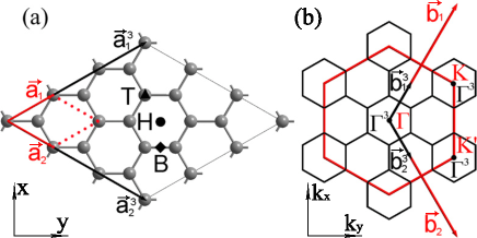
In Fig. 3 (a) we schematically plot the supercell of graphene compared to the supercell of graphene, with and representing the primitive vectors for the and supercells. Panel (b) illustrates the Brillouin zone of the supercell comparing to that of the supercell. One can note that the original valleys and are folded into the same point in the supercell of graphene, which makes the two valleys indistinguishable.
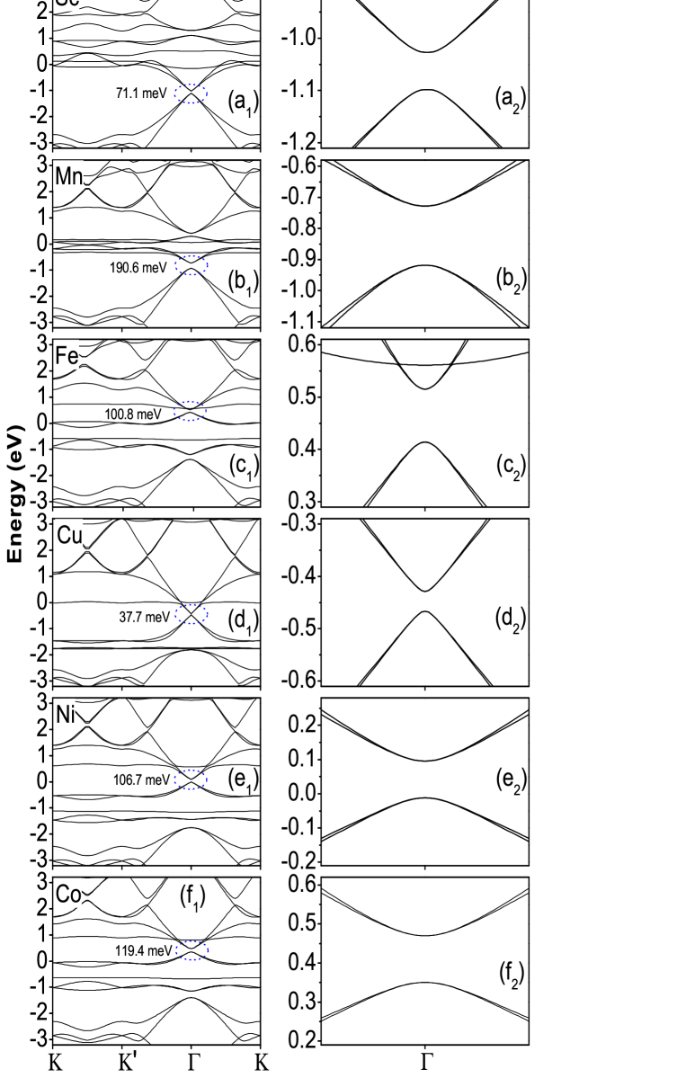
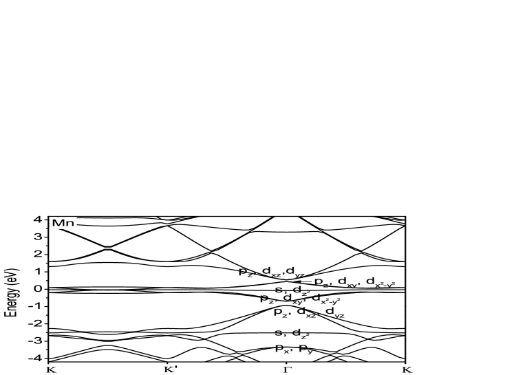
Figure 4 exhibits the band structures of supercells of graphene adsorbed with (a) Sc, (b) Mn, (c) Fe, (d) Cu, (e) Ni and (f) Co adatoms on top of the hollow position without involving spin degrees of freedom, i.e. nonmagnetic calculation. In the first column [i.e. panels ()-()], we plot the full band structures along the high symmetry lines. From the band structures shown in the second column [i.e. panels ()-()], the zooming in of the circled bands in the first column, we observe that large band gaps can open at the point due to the inter-valley scattering between and valleys, i.e. in units of for the supercell of graphene adsorbed with Sc, Mn, Fe, Cu, Ni, and Co, respectively. This is completely distinct from that of the adsorption on the supercells of graphene in the main text, where the perfect Dirac-cone dispersion holds at both and points. In our calculations we have used the Hydrogen atom to saturate the dangling bond of Mn atom, because in the Mn-adsorption the dangling d-band is properly located inside the resulting bulk gap. In the first column one can see that there are two bulk band gaps opened at the points. As shown in Fig. 5 the projected band analysis points out that the two gaps are essentially equivalent by combining the same orbital components of , and (or , and ).
Similar to the adsorption on the supercell of graphene, when the magnetization is included, the spin up (down) bands are upward (downward) shifted (see Figure 6). This results in three possible results: (i) As plotted in panels (a2)-(c2) and (f2) for Sc, Mn, Fe, and Co adsorption, the induced magnetization is so large (i.e. =0.213, 0.432, 1.080, 0.442 in units of eV) that the original band gaps from the inter-valley scattering are closed due to the crossover between the spin-down bands from the conduction bands and the spin-up bands from the valence bands. (ii) For panel (d2) of Cu-adsorption, the magnetization is moderately large (i.e. =0.035 eV) that the band gaps are just slightly decreased but not closed. (iii) For the Ni-adsorption in panel (e2) the band structure is exactly the same as that shown in Fig. 4 (e2) because there is no magnetization of graphene induced from the Ni adsorption.
When the spin-orbit coupling is further considered, we find that non-trivial band gaps can open at the crossing points between the spin-up and spin-down bands [see panels ()-() and () in Fig. 7], which shows similar origin as that in the adsorption on the supercells in the main text. However, we find that only the bulk band gaps in panels (-) are globally opened for Sc ( meV) and Mn ( meV), while that for Fe and Co in panels () and () are just locally opened. Therefore in the following, we will only focus on the nontrivial topological properties for Sc and Mn adsorption. Through calculating the Berry curvatures along the high symmetry lines for all the valence bands below the bulk gap, we find that all the Berry curvatures share the same sign as shown in panels () and (), resulting in the non-vanishing Chern number . By integrating all the Berry curvatures below the band gaps, our calculation shows that for the Sc/Mn adsorption. This again signals a QAH insulating state for the energies inside the bulk gap which will be explained in detail in Section II. Since the Fermi energy is not located inside the band gap, one has to apply external gate voltage to adjust the Fermi level inside the band gap to realize the insulating state. While for the other two adsorption of Cu and Ni shown in panels (d2)-(e2), we can see that the spin-orbit coupling further decreases the bulk gaps.
In summary, using the first-principles calculation methods, we find that for the supercell of graphene adsorbed with atoms (i.e. Sc, Mn, Fe, Cu, Ni) on the top of hollow position, trivial bulk band gaps can open at the point due to the inter-valley scattering without considering the spin degrees of freedom. For some particular adatoms (i.e. Sc, Mn) when the magnetization and spin-orbit coupling are involved, we find that non-trivial bulk band gaps can open around the point to realize the QAH effect. This finding not only generalizes our proposal of QAH effect in the supercell to the supercell of graphene, but also enhances the experimental realizability of the first QAH effect in graphene.
Appendix C Definitions of Quantum Anomalous Hall and Quantum valley Hall effects
C.1 Quantum Anomalous Hall Effect
The breaking of the time-reversal symmetry is a necessary condition for the formation of the Hall effects. In general, there are two kinds of methods breaking the time-reversal symmetry: the external magnetic field and the intrinsic magnetization of the ferromagnetic materials. When the two-dimensional electron gas is subjected to a strong perpendicular magnetic field, Laudau-levels can be formed to exhibit the integer quantum Hall effect with the Hall conductance exactly quantized in units of Klitzing . The precise quantization of Hall conductance can be understood in terms of a topological invariant known as the Chern number , which must be an integer PhysicsToday . Therefore the integer quantum Hall conductance can be expressed as:
| (2) |
Contrary to the ordinary Hall effect due to the magnetic field, the intrinsic magnetization induced Hall effect is termed as anomalous Hall effect. Though this anomalous Hall phenomenon has been known for over one century, its origin is still unclear AHE1 ; AHE2 . The quantized version of the anomalous Hall effect, also named as quantum anomalous Hall (QAH) effect, was first theoretically proposed by Haldane in a Honeycomb toy model after the experimental observation of the integer quantum Hall effect in 1980s haldane . However, the QAH effect is still not observed in experiment.
In our work on the metal adatom-graphene structures, we find that the QAH state can be observed in both and supercells of graphene. In the main text the bulk gaps are opened at both and points when the magnetization and spin-orbit coupling are considered. Because the Berry curvatures near and for the supercell show the same sign, therefore the summation of the Berry curvatures of the whole Brilloin-zone is finite, which indicates that the Chern number must be a nonzero integer. Since we do not apply any external magnetic field, therefore we can conclude this non-vanishing Chern number corresponds to the QAH state. Surprisingly, in the Section I of this supplementary materials we further find that the adsorption on the supercell can also contribute to the QAH effect through opening a nontrivial bulk band gap near the point by involving the magnetization and spin-orbit coupling.
C.2 Quantum Valley-Hall Effect
Quantum valley Hall (QVH) effect is named after the integer quantized but canceling quantum-Hall responses at and valley points. This effect can be arisen from the inversion-symmetry breaking, i.e. applying staggered AB sublattice potentials on the single layer graphene QVH3 , or considering gated bilayer graphene QVH1 . In terms of Chern number representation, but the total Chern number of the system is . One has to note that there is no edge modes for the QVH effect in the single layer graphene QVH2 ; QVH3 , while for the bilayer graphene there is indeed gapless edge states inside the bulk band gap QVH4 . These edge states are robust against smooth-type disorders, which is protected by the large momentum separation between two valleys.
In our studied adatom-/ structures, no QVH state can exist in the supercell systems because of the inter-valley scattering which makes valleys indistinguishable. In the supercell with noble atom adsorbed graphene systems, our calculation shows that the Berry curvatures at and are non-vanishing and opposite, which indicates that valleys and correspond to two opposite nonzero Chern numbers. Based on the definition of QVH effect, we can claim that our finding of the noble adatom adsorption on top of the supercell leads to the QVH effect.
References
- (1) K. von Klitzing, G. Dorda, M. Pepper, Phys. Rev. Lett. 45, 494 (1980).
- (2) J. E. Avron, D. Osadchy, and R. Seiler, Physics Today, 56, 38 (2003).
- (3) N. Nagaosa, J. Sinova, S. Onoda, A. H. MacDonald, and N. P. Ong, Rev. Mod. Phys. 82, 1539 (2010).
- (4) D. Xiao, M.-C. Chang, and Q. Niu, Rev. Mod. Phys. 82, 1959 (2010).
- (5) F. D. M. Haldane, Phys. Rev. Lett. 61, 2015 (1988).
- (6) D. Xiao et al., Phys. Rev. Lett. 99, 236809 (2007)
- (7) J. B. Oostinga, H. B. Heersche, X. Liu, A. F. Morpurgo, L. M. K. Vandersypen, Nat. Mat. 7, 151 (2007).
- (8) P, Ghaemi, S. Ryu, D.-H. Lee, Phys. Rev. B 81, 081403(R) (2010).
- (9) W.-K. Tse et al., Phys. Rew. B 83, 155447 (2011).