Strong back-action of a linear circuit on a single electronic quantum channel
What are the quantum laws of electricity in mesoscopic circuits? This very fundamental question has also direct implications for the quantum engineering of nanoelectronic devices. Indeed, when a quantum coherent conductor is inserted into a circuit, its transport properties are modified. In particular, its conductance is reduced because of the circuit back-action. This phenomenon, called environmental Coulomb blockade, results from the granularity of charge transfers across the coherent conductorIngold & Nazarov (1992). Although extensively studied for a tunnel junction in a linear circuitDevoret et al. (1990); Girvin et al. (1990); Cleland et al. (1992); Holst et al. (1994), it is only fully understood for arbitrary short coherent conductors in the limit of small circuit impedances and small conductance reductionYeyati et al. (2001); Golubev & Zaikin (2001); Altimiras et al. (2007). Here, we investigate experimentally the strong back-action regime, with a conductance reduction of up to 90%. This is achieved by embedding a single quantum channel of tunable transmission in an adjustable on-chip circuit of impedance comparable to the resistance quantum at microwave frequencies. The experiment reveals important deviations from calculations performed in the weak back-action frameworkYeyati et al. (2001); Golubev & Zaikin (2001), and matches with recent theoretical resultsKindermann & Nazarov (2003); Safi & Saleur (2004). From these measurements, we propose a generalized expression for the conductance of an arbitrary quantum channel embedded in a linear circuit.
The transport properties of a coherent conductor depend on the surrounding circuit. First, electronic quantum interferences blend the conductor with its vicinity, resulting in a different coherent conductor (see e.g. ref. Umbach et al. (1987)). In addition, the circuit back-action modifies the full counting statistics of charge transfers across coherent conductorsKindermann & Nazarov (2003); Safi & Saleur (2004); Golubev et al. (2005). This mechanism, which is our concern here, results in violations of the classical impedance composition laws even for distinct circuit elements, separated by more than the electronic phase coherence length. The present experimental work investigates the strong circuit back-action on the conductance of an arbitrary electronic quantum channel.
The circuit back-action originates from the granularity in the transfer of charges across a coherent conductor. Due to Coulomb interactions, an excitation by these current pulses of the circuit electromagnetic modes is possible, which impedes the charge transfers and therefore reduces the conductance of the coherent conductor. This environmental Coulomb blockade is best understood in the limit of a tunnel junction embedded in a circuit of very high series impedance, which is of particular importance for single electron devicesDevoret et al. (1992). In this limit, each time an electron tunnels across the junction, its charge stays a very long time on the capacitor inherent to the junction’s geometry. Consequently, a charging energy has to be paid. Since this energy is not available at low voltages and temperatures, the tunneling of electrons is blocked and the tunnel junction’s conductance vanishes. One speaks of ‘static’ Coulomb blockade, because the circuit’s dynamical response can be ignored. If now the circuit response time is short enough, the charging energy becomes ill-defined, with an uncertainty . This ‘dynamical’ Coulomb blockade regime corresponds to quantum fluctuations of the charge on the capacitor that are comparable to the electron charge . It is therefore essential to consider the circuit as a quantum object. For a resistor in series with the tunnel junction, the cross-over between the static and the dynamical Coulomb blockade is at . Importantly, the conductance can also be fully suppressed in the dynamical regime, at sufficiently low energy.
The environmental Coulomb blockade was first studied on small, opaque tunnel junctions embedded in linear circuitsDevoret et al. (1990); Girvin et al. (1990); Cleland et al. (1992); Holst et al. (1994). The studies were later extended to tunnel junctions of larger conductanceJoyez et al. (1998) and sizePierre et al. (2001), and to the high frequency domainHofheinz et al. (2011). To go beyond tunnel junctions, a major theoretical difficulty is that a general coherent conductor, with electronic channels of arbitrary transmission probabilities, cannot be handled as a small perturbation to the circuit. This difficulty was first overcome in the limit of low-impedance linear circuits with a small back-action. In this case, the striking predictionYeyati et al. (2001); Golubev & Zaikin (2001) and observationAltimiras et al. (2007) are that the circuit back-action on the conductance is directly proportional to the amplitude of quantum shot noise in absence of the circuit. However, the even more important and challenging regime of strong back-action remains mostly unexplored and unsolved for arbitrary coherent conductors, despite important advances in that directionMatveev et al. (1993); Molenkamp et al. (1995); Nazarov (1999); Kindermann & Nazarov (2003); Golubev et al. (2005) and a powerful link established with the Luttinger physics of interacting 1D conductorsSafi & Saleur (2004). The present experimental work investigates this regime on a tunable quantum point contact (QPC) embedded in an on-chip circuit of impedance comparable to , beyond reach of perturbative theoretical treatments, resulting in relative reductions of the QPC conductance of up to 90%.
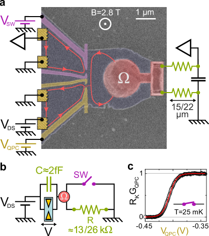
The samples are constituted of three basic elements (see Fig. 1a,b): (i) a tunable single electronic channel as a test-bed for coherent conductors, (ii) an on-chip dissipative environment and (iii) a switch to short-circuit the dissipative environment.
(i) We emulate any single-channel short coherent conductor with a tunable QPC formed by field effect in a buried GaAs/Ga(Al)As two-dimensional electron gas (2DEG), using a surface metallic split gate biased at (bottom split gate in Fig. 1a). A single-channel short coherent conductor is characterized by the ‘intrinsic’ quantum channel transmission probability , with the coherent conductor’s conductance in the absence of circuit back-action. The single step followed by a well-defined plateau of the QPC conductance (symbols in Fig. 1c) shows that the studied QPC can be operated in the single-channel regime, and that its transmission probability can be varied continuously from 0 to 1. The canonical QPC behavior is confirmed by fitting the measured with the standard saddle-point model of a QPCBüttiker (1990) (continuous line in Fig. 1c). Note that it is important to break spin degeneracy in order to first study a single electronic channel. Otherwise, the additional channels would partly shunt the surrounding circuitJoyez et al. (1998); Bagrets & Nazarov (2005). For this purpose, we applied a strong perpendicular magnetic field B=2.8 T corresponding to the integer quantum Hall effect at filling factor 4. Consequently, the current propagates at the edges along four copropagating edge channels. The studied outer edge channel is shown in Fig. 1a as a red line, with an arrow indicating the propagation direction. The three other edge channels (not shown) are always fully reflected at the QPC.
(ii) The second element is the QPC’s surrounding circuit, of large dissipative impedance up to microwave frequencies . This is achieved with a nanofabricated on-chip environment modeled by a linear RC circuit in Fig. 1b. The series resistances is for the sample shown in Fig. 1a and for a second sample. It is realized by two parallel thin chromium wires of identical lengths m (m) for () deposited at the surface. These chromium wires can be described as macroscopic linear resistors (see Supplementary Information). The parallel capacitance in Fig. 1b corresponds to the shunt capacitor to AC ground of the area delimited by the metal split gates and the series chromium wires. To avoid a capacitive short-circuit of the series resistance at the relevant microwave frequencies, this area must be minimized. For this purpose, the buried 2DEG is connected to the chromium resistors at the surface with a micron-scale AuGeNi ohmic contact (labeled in Fig. 1a). This micron-scale contact also plays the role of a floating electron reservoir, which breaks the quantum coherence between electrons emitted and arriving at the studied QPC.
(iii) The third element is a switch that allows us to suppress the back-action of the environment by short-circuiting it. This switch is controlled by the voltage applied to the top split gate in Fig. 1a. A second voltage amplifier (top-left in Fig. 1a) is used to monitor the switch’s conductance.
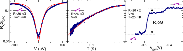
In the present experiment, the reduction of the QPC conductance by the circuit back-action is extracted by three different methods: We measure as a function of either the DC voltage across the QPC (Fig. 2, left panel), the temperature (Fig. 2, center panel), or the gate voltage controlling the switch (Fig. 2, right panel). In the first two methods, traditionally used to investigate the Coulomb blockade, is obtained by assuming that converges toward its ‘intrinsic’ conductance for or much larger than and . In the third method, is obtained from the QPC conductance measured with a short-circuited environmental impedance. This last, more direct method yields the back-action signal without any particular assumption on its energy dependence, and avoids possible sources of errors related to the transmission energy dependence, sample heating, or the QPC stability over long times.
Figure 2 illustrates the three methods for the same sample of series resistance , and with the QPC set to similar low transmissions. In this near-tunnel limit, the measured voltage and temperature dependence of , shown as symbols in the left and center panels, can be compared with the known predictions for tunnel junctionsIngold & Nazarov (1992). The calculations plotted as continuous lines were performed within the simplified RC model depicted in Fig. 1b. The temperature was set to that of the dilution fridge mixing chamber, to the measured value of the on-chip series resistance, and the parallel geometrical capacitance to the value fF obtained by finite element numerical simulations. The only fit parameter is the transmission in absence of back-action (left panel) and 0.19 (center panel). The right panel shows versus the voltage controlling the switch to short-circuit the environment. The capacitive cross-talk between the switch gates and the QPC gates was first calibrated for each sample, then compensated for when sweeping (see Supplementary Information). For V, the conductance across the switch is zero, and the measured corresponds to the conductance reduced by the environmental back-action. As is increased, the switch’s conductance increases in steps corresponding to the successive edge channels transmission. The environmental back-action is found to be suppressed by fully transmitting the two outer edge channels across the switch (see Supplementary Information); the corresponding QPC conductance measured at V is taken as . We stress that the conductance reductions obtained from all three methods are consistent with one another, and that we find a good agreement between data and theoretical predictions in the tunnel limit for a known surrounding circuit. This provides strong support for our interpretation of in terms of environmental back-action. We have now established the experimental principle with a tunnel QPC, and demonstrated the strong back-action regime with a conductance reduction of .
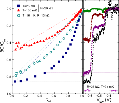
Next, we investigate the circuit back-action on an arbitrary single-channel coherent conductor characterized by its ‘intrinsic’ transmission probability . The left panel of Fig. 3 shows as symbols, for both samples, the measured relative reduction of the QPC conductance due to the circuit back-action when the switch is open, as a function of . The right panel shows the sweeps at for the sample at 25 mK. First, we observe that is largest in the tunnel limit and diminishes monotonously toward zero as increases toward full transmission. However, contrary to predictions and observations in the limit of small environmental impedancesYeyati et al. (2001); Golubev & Zaikin (2001); Altimiras et al. (2007), is not proportional to in the full range (dashed lines), but markedly larger at intermediate . As seen by comparing the data at T=25 mK and 100 mK for the sample, when the temperature increases, and the deviations to a dependence decrease.
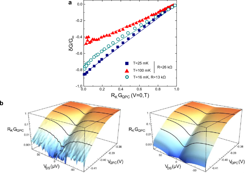
Remarkably, we observe that the back-action correction to the conductance is instead proportional to , for all series resistances and temperatures. This is demonstrated, within experimental uncertainties, in Fig. 4a by plotting now as a function of . This proportionality can be written as , where is the relative circuit back-action for a small tunnel junction embedded in the same circuit. Using the environmental Coulomb blockade framework for tunnel junctionsIngold & Nazarov (1992), can be calculated for arbitrary circuit impedances , bias voltages and temperatures . Consequently, solving the above equation for allows us to propose a generalized expression for the conductance of a single electronic channel of arbitrary transmission embedded in a linear environment of arbitrary impedance (see also Supplementary Information):
| (1) |
We further tested the proposed equation 1 by comparing in Fig. 4b the measured (left panel) and calculated (right panel) QPC conductance versus the applied bias voltage and the gate voltage for . The calculations were performed with Eq. 1 using . We find a good agreement between data and theory for , illustrating the validity of this formula even at finite bias voltage. Note that for , we find that the measured dip in is significantly narrower than calculations. However, this deviation can be accounted for by including the significant sample heating by the DC current within a simplified model based on the Wiedemann-Franz law (see Supplementary Information).
Moreover, equation 1 agrees with a recent theoretical prediction using a renormalization-group approachKindermann & Nazarov (2003) (see Supplementary Information), and generalizes it to arbitrary impedances, beyond resistances small compared to .
Equation 1 could be understood as a direct link between the conductance reduction by the circuit back-action and the quantum shot noise in presence of the circuit. The bridge established for a purely resistive environment between Luttinger physics and environmental Coulomb blockade suggests that remains proportional to the amplitude of quantum shot noise for arbitrary series impedancesSafi & Saleur (2004). As pointed out in ref. Safi & Saleur (2004), the quantum shot noise is now strongly modified by the environmental back-action. Although there is no fully developed theoretical framework, the experimental observation , from which Eq. 1 is derived, would correspond to a quantum shot noise spectral density of the current in presence of back-action that verifies . Significantly, the same expression is verified in absence of circuit back-actionMartin & Landauer (1992); Blanter & Büttiker (2000), but using the ‘intrinsic’ transmission probability instead of the measured transmission probability . These relations can be derived exactly in the special case (private comm. I. Safi).
To conclude, we explored the strong back-action of a linear circuit on an arbitrary, single-channel, short coherent conductor. The results suggest the generalized expression Eq. 1 for the environmental back-action, which remains to be derived theoretically. This experiment opens the path for further inquiries of the quantum laws of electricity in nanocircuits. These include the investigation of circuits with coherent conductors in which the environmental back-action can coexist with other phenomena such as the Kondo effectFlorens et al. (2007), as well as the investigation of the circuit back-action on the full statistics of charge transfers across a coherent conductorKindermann & Nazarov (2003); Safi & Saleur (2004); Golubev et al. (2005).
Methods
The measurements were performed in a dilution refrigerator down to mK, on two samples tailored in a typical 2DEG. The 2DEG of density and mobility is buried 94 nm deep in a GaAs/Ga(Al)As heterojunction. The measured differential conductances were obtained by standard lock-in techniques at frequencies below Hz with custom-made ultra-low noise electronics. In order to measure independently the QPC conductance and the series resistance , and also to test the small ohmic contact, the end of one of the chromium wires realizing is connected at room temperature to a high impedance voltage amplifier (see Fig. 1a). Due to antenna effects, the impedance of the line toward the amplifier is reduced at the relevant microwave frequencies to about the vacuum impedance . This is symbolized in Fig. 1a by a capacitor in parallel with the top-right amplifier. Further details are given in the Supplementary Information.
References
- Ingold & Nazarov (1992) Ingold, G.-L. & Nazarov, Y. Single charge tunneling; Coulomb blockade phenomena in nanostructures (1992), plenum, new york edn. (Chapter 2).
- Devoret et al. (1990) Devoret, M. H. et al. Effect of the electromagnetic environment on the Coulomb blockade in ultrasmall tunnel junctions. Phys. Rev. Lett. 64, 1824–1827 (1990).
- Girvin et al. (1990) Girvin, S. M., Glazman, L. I., Jonson, M., Penn, D. R. & Stiles, M. D. Quantum fluctuations and the single-junction Coulomb blockade. Phys. Rev. Lett. 64, 3183–3186 (1990).
- Cleland et al. (1992) Cleland, A. N., Schmidt, J. M. & Clarke, J. Influence of the environment on the Coulomb blockade in submicrometer normal-metal tunnel junctions. Phys. Rev. B 45, 2950–2961 (1992).
- Holst et al. (1994) Holst, T., Esteve, D., Urbina, C. & Devoret, M. H. Effect of a Transmission Line Resonator on a Small Capacitance Tunnel Junction. Phys. Rev. Lett. 73, 3455–3458 (1994).
- Yeyati et al. (2001) Yeyati, A. L., Martin-Rodero, A., Esteve, D. & Urbina, C. Direct Link between Coulomb Blockade and Shot Noise in a Quantum-Coherent Structure. Phys. Rev. Lett. 87, 046802 (2001).
- Golubev & Zaikin (2001) Golubev, D. S. & Zaikin, A. D. Coulomb Interaction and Quantum Transport through a Coherent Scatterer. Phys. Rev. Lett. 86, 4887–4890 (2001).
- Altimiras et al. (2007) Altimiras, C., Gennser, U., Cavanna, A., Mailly, D. & Pierre, F. Experimental Test of the Dynamical Coulomb Blockade Theory for Short Coherent Conductors. Phys. Rev. Lett. 99, 256805 (2007).
- Kindermann & Nazarov (2003) Kindermann, M. & Nazarov, Y. V. Interaction Effects on Counting Statistics and the Transmission Distribution. Phys. Rev. Lett. 91, 136802 (2003).
- Safi & Saleur (2004) Safi, I. & Saleur, H. One-Channel Conductor in an Ohmic Environment: Mapping to a Tomonaga-Luttinger Liquid and Full Counting Statistics. Phys. Rev. Lett. 93, 126602 (2004).
- Umbach et al. (1987) Umbach, C. P., Santhanam, P., van Haesendonck, C. & Webb, R. A. Nonlocal electrical properties in mesoscopic devices. Appl. Phys. Lett. 50, 1289–1291 (1987).
- Golubev et al. (2005) Golubev, D. S., Galaktionov, A. V. & Zaikin, A. D. Electron transport and current fluctuations in short coherent conductors. Phys. Rev. B 72, 205417 (2005).
- Devoret et al. (1992) Devoret, M. H., Esteve, D. & Urbina, C. Single-electron transfer in metallic nanostructures. Nature 360, 574–553 (1992).
- Joyez et al. (1998) Joyez, P., Esteve, D. & Devoret, M. H. How Is the Coulomb Blockade Suppressed in High-Conductance Tunnel Junctions? Phys. Rev. Lett. 80, 1956–1959 (1998).
- Pierre et al. (2001) Pierre, F. et al. Electrodynamic Dip in the Local Density of States of a Metallic Wire. Phys. Rev. Lett. 86, 1590–1593 (2001).
- Hofheinz et al. (2011) Hofheinz, M. et al. Bright Side of the Coulomb Blockade. Phys. Rev. Lett. 106, 217005 (2011).
- Matveev et al. (1993) Matveev, K. A., Yue, D. & Glazman, L. I. Tunneling in one-dimensional non-Luttinger electron liquid. Phys. Rev. Lett. 71, 3351–3354 (1993).
- Molenkamp et al. (1995) Molenkamp, L. W., Flensberg, K. & Kemerink, M. Scaling of the Coulomb Energy Due to Quantum Fluctuations in the Charge on a Quantum Dot. Phys. Rev. Lett. 75, 4282–4285 (1995).
- Nazarov (1999) Nazarov, Y. V. Coulomb Blockade without Tunnel Junctions. Phys. Rev. Lett. 82, 1245–1248 (1999).
- Büttiker (1990) Büttiker, M. Quantized transmission of a saddle-point constriction. Phys. Rev. B 41, 7906–7909 (1990).
- Bagrets & Nazarov (2005) Bagrets, D. A. & Nazarov, Y. V. Full Current Statistics in the Regime of Weak Coulomb Interaction. Phys. Rev. Lett. 94, 056801 (2005).
- Martin & Landauer (1992) Martin, T. & Landauer, R. Wave-packet approach to noise in multichannel mesoscopic systems. Phys. Rev. B 45, 1742–1755 (1992).
- Blanter & Büttiker (2000) Blanter, Y. M. & Büttiker, M. Shot Noise in Mesoscopic Conductors. Physics Reports 336, 1–166 (2000).
- Florens et al. (2007) Florens, S., Simon, P., Andergassen, S. & Feinberg, D. Interplay of electromagnetic noise and Kondo effect in quantum dots. Phys. Rev. B 75, 155321 (2007).
Acknowledgments
The authors gratefully acknowledge Y. Nazarov, the Quantronics group and I. Safi for discussions, F. Lafont for his contribution to the experiment, and L. Couraud and C. Ulysse for their contributions to the nano-fabrication. This work was supported by the ERC (ERC-2010-StG-20091028, #259033), the ANR (ANR-09-BLAN-0199) and NanoSci-ERA (ANR-06-NSCI-001).
Author contributions
Experimental work and theoretical analysis: A.A., F.D.P., F.P. and S.J.; nano-fabrication and sample design: A.A., F.P. and H.l.S. with inputs from D.M.; heterojunction growth: A.C. and U.G.; manuscript preparation: A.A., F.D.P., F.P. and U.G. with inputs from coauthors; project planning and supervision: F.P.
Additional information
Supplementary Information accompanies this paper. Correspondences and requests for materials should be addressed to A.A. and F.P.