Current-Conserving Aharonov-Bohm Interferometry with Arbitrary Spin Interactions
Abstract
We propose a general scattering matrix formalism that guarantees the charge conservation at junctions between conducting arms with arbitrary spin interactions. By using our formalism, we find that the spin-flip scattering can happen even at nonmagnetic junctions if the spin eigenstates in arms are not orthogonal. We apply our formalism to the Aharonov-Bohm interferometer consisting of -type semiconductor ring with both the Rashba spin-orbit coupling and the Zeeman splitting. We discuss the characteristics of the interferometer as conditional/unconditional spin switch in the weak/strong-coupling limit, respectively.
pacs:
73.63.-b, 73.23.-b, 71.70.Ej, 03.65.VfI Introduction
Coherent electronic transport through mesoscopic rings or structures with non-trivial geometries has been extensively investigated both theoretically Buttiker1984oct ; Loss1990sep ; Loss1992jun ; Yi1997apr ; Romer2000sep ; KangK2000dec ; Frustaglia2001nov ; Meijer2002jul ; Hentschel2004apr ; Frustaglia2004jun ; Wang2005oct ; LeeMC2006feb ; Lucignano2007jul ; Kovalev2007sep ; Pletyukhov2008may ; Borunda2008dec ; Stepanenko2009jun and experimentally Umbach1984oct ; Webb1985jun ; Bergsten2006nov ; Habib2007apr ; Grbic2007oct ; Qu2011jun in last decades. The studies have aimed at exploring theoretically the quantum interference in solid-state circuits and also revolutionizing electronic devices in such a way to exploit the quantum effects. At the heart of studies of mesoscopic rings, there are two hallmarks of quantum coherence: the Aharonov-Bohm Aharonov1959aug (AB) and Aharonov-Casher Aharonov1984jul (AC) effects. Two effects are related to geometric phases due to the coupling of a charge to a magnetic flux and of a spin degree of freedom to an electric field via spin-orbit coupling (SOC), respectively. Since the AB oscillation in conductance through normal-metal rings was revealed, Buttiker1984oct it is found that the effects can lead to diverse quantum interference effects such as conductance fluctuations, Umbach1984oct persistent charge and spin current, Loss1990sep ; Loss1992jun AB effect for exciton, Romer2000sep mesoscopic Kondo effect, KangK2000dec spin switch, Frustaglia2001nov ; Frustaglia2004jun spin filter, LeeMC2006feb and spin Hall effect. Borunda2008dec From a practical point of view, the quantum coherent phenomena in mesoscopic rings, especially using the spin degrees of freedom, have been applied to the fast growing field of spintronics Wolf2001nov ; Zutic2004apr and are now known to provide the easy-to-control devices that generate, manipulate, and detect the spin-dependent current or signal.
Mesoscopic rings fabricated in semiconductors offer intriguing possibility to study simultaneously the AB and AC effects because of spin-orbit coupling naturally formed in crystals. The spin-orbit coupling itself can have various forms in different materials, leading to diverse current oscillations.Frustaglia2004jun ; Habib2007apr ; Grbic2007oct In addition, the strength of the spin-orbit coupling can be controlled by tuning a backgate voltage to the device. Nitta1997feb Among spin-orbit couplings, the Rashba SOC, originating from the broken structural inversion symmetry, is linear in momentum and easy to analyze. The studies of spin interference Meijer2002jul ; Frustaglia2004jun subject to the Rashba SOC have shown that the Rashba coupling strength can modulate the unpolarized current, suggesting the possibility of all-electrical spintronic devices. Recently, a number of experimental Habib2007apr ; Grbic2007oct and theoretical Kovalev2007sep ; Borunda2008dec ; Stepanenko2009jun studies have investigated transport of heavy holes in rings, whose SOC is cubic in momentum. In the presence of external magnetic fields, the Zeeman splitting is operative together with the SOCs and its effect should be taken into account. Yi1997apr ; Frustaglia2001nov ; Hentschel2004apr ; Wang2005oct ; Lucignano2007jul
The general framework for the theoretical studies of the mesoscopic transport relies on the Landauer approach, Datta1995 and it is described as tunneling through conduction modes between the source and drain electrodes coupled to rings. In the coherent regime, the tunneling is accompanied by interference between conduction modes. The conductance is then described by a scattering matrix between modes that carry distinct phases. Due to interference, the fact that each of the modes is charge conserving does not guarantee the charge conservation in the total transport. More specifically, a problem arises when the ring modes form nonorthogonal spin textures; the spins of the states with the same energy are not orthogonal at every point. Such a complexity does not arise if the ring has either of the linear-in-momentum SOCs (like the Rashba SOC) or the Zeeman splitting because one can then diagonalize the system Hamiltonian such that no mode mixing takes place. However, in realistic situations with arbitrary form of SOC and Zeeman splitting, the mode mixing, or spin mixing, naturally exists.
The previous studies considering both the effect of the Rashba SOC and the Zeeman splitting have dealt with this situation by using the transfer-matrix method accompanied with wave function matching, Yi1997apr ; Frustaglia2001nov ; Hentschel2004apr perturbative approach, Wang2005oct and path-integral approach. Lucignano2007jul The transfer-matrix method, even though different group velocities of ring modes are taken into account, fails guaranteeing the charge conservation at the lead-ring junction. In their studies, the relation between the lead and the ring modes are determined solely by the wave function matching, which alone cannot satisfy the charge conservation. The perturbative calculation is valid only in the small Zeeman splitting limit. Finally, the path-integral approach, which may be conceptually useful to interpret the result in terms of phases, is limited by its semiclassical treatment.
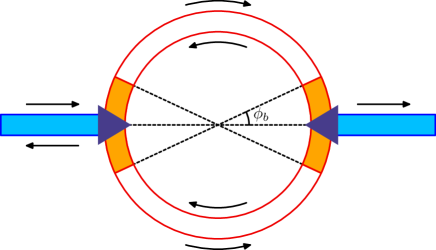
Our goal in this work is to find a general scattering matrix formalism that guarantees the charge conservation at the lead-ring junctions by its own way of construction in the presence of arbitrary spin interactions. We detour the mode mixing problem by introducing artificial spin-independent buffer regions in the vicinity of every junction as shown in Fig. 1. The mode-mixing effect is then taken care of at the interfaces between the buffers and the spinful regions in a standard way. Finally, the original system is recovered in the limit of vanishing buffers. By using our formalism, we first recover the known results in the case of orthogonal spin textures and interpret the role of buffers added by hand. Secondly, we apply our formalism to the -type semiconductor ring with both the Rashba SOC and the Zeeman splitting. We found that (1) our formalism truly guarantees the charge conservation at every junction, giving rise to correct predictions, (2) the spin-flip scattering can happen even if the junctions are nonmagnetic, (3) the ring interferometer can act as conditional/unconditional spin switch in the weak/strong-coupling regimes, respectively, if some conditions are met.
Our paper is structured as follows: Our formalism is introduced and derived in detail in Sec. II. In Sec. III the case of orthogonal spin texture is treated within our formalism. Section IV is devoted to the study of a case of nonorthogonal spin states in which both the Rashba SOC and the Zeeman splitting are taken into account. Finally, we conclude and summarize our paper in Sec. V.
II General Formalism to Build Current-Conserving Scattering Matrix
II.1 Buffered Structure
The scattering in the mesoscopic system is frequently characterized in terms of the scattering matrix which defines the relative amplitudes and phases of the scatted states to the injected states. The scattering matrix depends on the details of the system but is constrained by the laws of conservation. The most important properties that the scattering matrix obeys are the current conservation, if there is neither a source or a sink in scatterer and, additionally the spin current conservation, if the scatterer is nonmagnetic. The conservation conditions, together with some symmetric arguments, quite simplify the form of the scattering matrix so that it can be described by a few parameters. For example, the most frequently used scattering matrix for the AB interferometer is controlled by a single parameter that is varied between 0 (no tunneling) and 1/2 (perfect tunneling). Here the scattering to and from upper and lower arms is assumed to be symmetric.
This simple construction of the scattering matrix can be extended further to the magnetic case where spin-dependent interactions exist in the arms. In the presence of the Zeeman splitting, one can treat the scattering of spin up and down separately, each of which is described by the simple scattering matrix mentioned before. For the case of linear-in-momentum spin-orbit coupling such as the Rashba SOC, one can identify a common spin polarization axis at a junction so that spin-separate treatment is still possible. No difficulty in defining the scattering matrix that satisfies the conservation laws arises as long as all the arms meeting at a junction share a single spin polarization axis. However, the latter condition is quite fragile and generally fails in the presence of general spin-dependent interactions in the arms. The simplest case in which it happens is the ring with both the Rashba SOC and the Zeeman splitting. As will be shown later, the ring eigenstates are neither parallel or orthogonal to each other in the spin space at all, denying a common spin polarization axis. The scattering into the ring then involves all the spin states, preventing spin-separate treatment. The scattering matrix is then complicated although it should still fulfill the conservation laws.
One can then issue several questions. Is there a general framework to build the spin-dependent scattering matrix, which guarantees satisfying the conservation laws by the way of its construction? What is the smallest number of controlling parameters that are required to describe the scattering in the presence of arbitrary spin-dependent interactions? Can the spin-flip scattering happen even if the scatterer itself is still nonmagnetic?
In order to answer these questions we propose a general formalism to build up a consistent (spin-dependent) scattering matrix for arbitrary spin interaction. The key idea of our method is to insert artificial buffer regions between the scatter and arms as depicted in Fig. 1. The buffer regions are assumed to be free of any spin-dependent interaction. Hence, the scattering between buffer regions can be described by the simple spin-separate scattering matrix. The complexity due to the spin-dependent interaction makes its effect at interfaces between buffers and arms. The wave functions at interfaces are matched in the systematic way by using the continuity of wave function and its current density. This wave matching, together with the scattering matrix between buffer states, leads one to find the scattering matrix between states of arms. The size of artificial buffers is then shrunken to zero in order to recover the original configuration. The shrinking does not remove all the effects of buffers because the effect of scattering at buffer-arm interfaces still remains. In the end, the scattering matrix connecting states of arms is constructed.
The advantages of our methods are listed as follows: (1) The scattering matrix obtained guarantees satisfying the conservation laws. It is because the scattering between buffer states and the scattering at buffer-arm interfaces are set up to conserve the charge and spin currents. (2) It systematically identifies the minimal set of controlling parameters that the scatterer can have. (3) It provides the reasonable explanation for the effect of spin interactions in arms on the spin-dependent (possibly spin-flip) scattering even when the scatterer itself is nonmagnetic.
In the following sections we build up our formalism, especially focusing on the AB interferometer shown in Fig. 1. The system consists of two leads and one ring. Each part is assumed to be narrow enough to be regarded as one-dimensional conductor with a single transverse mode. The scattering matrix between lead and ring then becomes a matrix. We will construct a general scattering matrix for ring with arbitrary spin interaction. Our formalism, however, is quite general and can be applied to mesoscopic circuits with any kind of geometry.
II.2 Arms: Lead Part
The leads are composed of normal conductors directing along the direction. They are free of any magnetic interaction, and their Hamiltonians read
| (1) |
where is the effective mass of electrons in the leads and is the minimum energy of the transverse mode. Thanks to the spin degeneracy, the spin polarization axis of eigenstates can be chosen arbitrarily. Eigenstates of the leads with the eigenenergy then are given by
| (2) |
with the wave number and the spinors
| (3) |
Here is the spin index, and the lead index. The angles define the spin polarization axis for the injection from the left lead () and the spin detection axis in the right lead (), respectively. In terms of coefficients of injected (), reflected (), and transmitted () waves, the general wave functions in the leads are given by
| (4a) | ||||
| (4b) | ||||
where
| (5) |
and
| (6) |
The group velocities of the eigenstates are , and the charge current densities in the leads are
| (7) |
II.3 Arms: Ring Part
Ring can be either of normal conductor, -type semiconductor, or -type semiconductor. It is narrow enough that the radial dimension is constant with the radius and the degree of freedom is solely described by the azimuthal angle . We assume that an external magnetic field is applied so that the ring encloses a magnetic flux , or the dimensionless flux with the flux quantum and the spin splitting arises due to the Zeeman term
| (8) |
where is the Landé -factor, the Bohr magneton, and the Pauli matrices. For semiconductor rings, an appropriate spin-orbit interaction is operative. The ring Hamiltonian is then given by
| (9) |
with
| (10) |
where is the effective mass in the ring. In general the Hamiltonian has four eigenstates labeled by the spin index and the propagation direction (counterclockwise) and (clockwise) for each energy . Each eigenstate is endowed with a wave number , the solution of the dispersion relation. The wave number can be real (propagating state) or complex number (evanescent wave). The general form of the eigenstates is then written as
| (11) |
In terms of coefficients for the upper arm (U) and for the lower arm (D), the ring wave functions are given by
| (12a) | ||||
| (12b) | ||||
where
| (13) |
and
| (14) |
The group velocity of each eigenstate, is given by the expectation value of the velocity operator . Note that the spin-orbit interaction affects the velocity operator, and in general the energy eigenstate is not the eigenstate of the velocity operator. If the time reversal symmetry is not broken, the relations and hold generally no matter what the spin-orbit interaction is. In terms of the group velocities, the charge current densities in the ring are expressed as
| (15a) | ||||
| (15b) | ||||
for the upper and lower arms, respectively. For later use, we define the wave function applied by the velocity operator
| (16a) | ||||
| (16b) | ||||
where the matrix depends on the details of the system.
II.4 Buffers
In our formalism, no buffer region is inserted between the leads and the junctions. It is because the leads are free of spin-dependent interaction like buffers and the scattering at the interface between the lead and the buffer becomes trivial. On the other hand, as shown in Fig. 1, the buffer regions are inserted between the junctions and the ring arms. In the AB interferometer, therefore, four buffer regions with the same angular size are defined in the left/right side of upper/lower arms. Having the junctions at the angles and , the interfaces between the buffers and the arms are located at , , , and . Since the buffers are free of any spin-dependent interaction like leads, the Hamiltonian in buffers reads
| (17) |
where is the offset in the band bottom with respect to the ring part. With no spin interaction, it is free to choose the spin polarization axes in them, and the axis of each buffer is chosen to that of the nearest-neighboring lead. Eigenstates of the buffers with the energy , labeled by and , are then given by
| (18) |
with the wave number and the nearby-lead index . By defining the coefficients for the upper buffers close to the side and for the lower buffers close to the side , the buffer wave functions are written as
| (19a) | ||||
| (19b) | ||||
where
| (20) |
and
| (21) |
The group velocities of the eigenstates are simply given by , which is the eigenvalue of the velocity operator , and the charge current densities in the buffers are
| (22a) | ||||
| (22b) | ||||
for the left/right and upper/lower buffers, respectively. For later use, we define the wave function applied by the velocity operator
| (23a) | ||||
| (23b) | ||||
II.5 Lead-Buffer Scattering Matrices
With the buffered structure, the scattering at the junctions connects the states in the leads and the buffers. Since both the leads and the buffers have no magnetic interaction, the conventional scattering matrix can be defined to describe the scattering at the junctions. The reasonable conditions for the scattering matrix are that (1) no spin flip takes place, (2) the scatterings from and to the upper and lower arms are same, (3) no phase shift is acquired, and (4) the charge current is conserved. The first condition makes the scattering matrix diagonal in the spin space, and due to the second condition the scattering matrix with respect to the normalized flux is symmetric in the exchange between the upper and lower arms. The most general lead-buffer scattering matrix satisfying the above conditions is then
| (24) |
with
| (25a) | ||||
| (25b) | ||||
| (25c) | ||||
| (25d) | ||||
with . Here the controlling parameter varies from 0 (perfect transmission) to 1/2 (complete decoupling), and is identity matrix, indicating the absence of spin-flip scattering. Throughout this paper, we set considering the case of phase-conserving scattering between upper and lower arms.
Assuming that both the junctions have the same scattering matrix, one can set up linear equations for the coefficients of lead and buffer states: at the left junction
| (26a) | ||||
| (26b) | ||||
and at the right junction
| (27a) | ||||
| (27b) | ||||
where the left- and right-moving buffer states are defined as
| (28) |
respectively.
Note that the form of the scattering matrix guarantees the charge and spin current conservation by the way of its construction.
II.6 Lead-Arm Scattering Matrices
Now we derive the scattering matrix connecting the lead states and the ring states. To do that, we need to find out the linear relations between the buffer states and the ring states. The relations are to be determined from the boundary conditions at the interfaces by using the continuity of wave function and the current conservation. The latter condition can be reformulated in terms of the continuity of where is the Hamiltonian defined simultaneously in the buffer and ring regions. As long as the spin-orbit interaction is composed of the linear and/or second orders of the momentum operator, the continuity of leads to the continuity of . Now we apply the boundary conditions at four interfaces. By using Eqs. (12) and (19), the continuity of the wave function, and at the interfaces gives rise to
| (29a) | ||||
| (29b) | ||||
The second continuity conditions, and , together with Eqs. (16) and (23), lead to
| (30a) | ||||
| (30b) | ||||
It is straightforward to solve the equations for the coefficients of the buffer states:
| (31a) | ||||
| (31b) | ||||
with
| (32) |
Once the relations between coefficients of the buffer and the ring states are set up, it is time to shrink the buffers by setting . The buffer propagating matrices, become the identity matrix just because of zero propagating distance. Here some caution should be made about the limit values of the interface points. The left interfaces go to the single point, , while the limit values of the right interfaces are different, and .
Combining Eqs. (26), (27), and (31), one can build linear equations for the coefficients of lead and ring states, which are similar to Eqs. (26) and (27): at the left junction
| (33a) | ||||
| (33b) | ||||
and at the right junction
| (34a) | ||||
| (34b) | ||||
where the left- and right-moving ring states and the propagating matrices are defined as
| (35) |
and
| (36) |
respectively. The lead-ring scattering matrices
| (37) |
are then given by
| (38a) | ||||
| (38b) | ||||
| (38c) | ||||
| (38d) | ||||
with
| (39a) | ||||||
| (39b) | ||||||
From Eqs. (38) and (39), a few immediate general features of the scattering matrix can be discussed: (1) In general, the matrices are not spin diagonal. It means that the lead-ring scattering matrices are not diagonal in the spin basis even if we start with the assumption that the junction itself does not invoke the spin-flip scattering. For example, the spin up injected from the lead can be reflected into the spin down for any spin injection axis. It is not because the junction is a magnetic scatterer but because of spin-dependent interaction in the ring. The magnetic property in the arms of the ring can invoke the spin-dependent scattering at the junctions. (2) The buffer effect remains. The lead-ring scattering matrix have two controlling parameters: and . The latter parameter enters into the scattering matrix in terms of the buffer group velocity . The velocity appears in the scattering matrix in two ways: in the overall factor of and [see Eq. (25)] and in the matrices [see Eq. (32)]. The overall factor appears in in the same way as in and does not affect the spin-dependent scattering discussed above. On the other hand, in the matrices can tune magnitudes of its off-diagonal components. Therefore, we can draw a conclusion that at least two parameters for junctions, here and , are necessary to specify and control the spin-dependent scattering due to arbitrary spin-dependent interaction in arms.
We’d like to emphasize that the scattering matrix, Eq. (38) is the only solution that guarantees the conservation of the charge and spin currents at junctions under our symmetric assumptions. Since we have used the simplest buffer structure that introduces only one additional parameter, more complexity, if necessary, can be introduced into the scattering matrix by allowing additional interactions in the buffer. Here we introduce the minimal scattering matrix working properly in the presence of general spin-orbit interaction.
II.7 Reflection and Transmission Coefficients
It is now quite straightforward to solve Eqs. (33) and (34) in order to obtain the spin-resolved reflection and transmission coefficients in terms of the lead-ring scattering matrix :
| (40a) | ||||
| (40b) | ||||
with
| (41a) | ||||
| (41b) | ||||
| (41c) | ||||
Note that the overall factors in and are canceled out in the reflection and transmission coefficients. Therefore, the velocity in the leads does not affect the coefficients at all.
Below we calculate the transmission amplitudes , and by using them the charge conductance
| (42) |
and the current polarization
| (43) |
with respect to unpolarized input current are obtained.
III Orthogonal Spin States
Before proceeding to study the case in which our formalism is indispensable, we want to apply it to the simple cases where the spin-separate treatment is possible. As mentioned in the previous section, the spin-separate treatment can be used when the ring is of the normal conductor, or has the linear-in-momentum spin-orbit coupling such as Rashba SOC, or has the Zeeman splitting only. What is in common in all the cases is that the group velocity and the spin matrix are direction-independent, and and that the energy eigenstates are also the eigenstates of the corresponding velocity operator,
| (44) |
( only when the Zeeman splitting exists). Then the matrix in Eq. (16) is simply given by
| (45) |
Accordingly, the matrices are simplified to
| (46) |
with
| (47) |
By setting (note that and usually differ only up to the overall phase factor), the matrices become spin diagonal, and consequently we recover the spin-separate lead-ring scattering matrix. For each spin component, the lead-ring scattering matrix for spin can be expressed as
| (48a) | ||||
| (48b) | ||||
| (48c) | ||||
| (48d) | ||||
The buffer effect due to the velocity mismatch at buffer-ring interfaces still remains in the above expressions. However, one can recover the original form of the scattering matrix by redefining the controlling parameter . In other words, one can easily prove that the above scattering matrix can be rewritten as
| (49) |
with
| (50) |
Note that for and , as expected. It implies that in the cases where the spin-separate treatment is possible the only role of the buffer is to renormalize the tunneling parameter through Eq. (50). Hence the buffer is unnecessary and the junction can be characterized by a single parameter of arbitrary values. However, our formalism reveals the possible origin of spin-dependent values for . The difference between for two spins is due to different group velocity in the ring and consequent difference in the magnitude of velocity mismatch at the junction. Even though it is convention in literature to define a same value of for two spins, it is more physically correct to have different tunneling parameters for two spin components, as shown in our formalism.
IV Nonorthogonal Spin States
As an application of our formalism, we consider the -type semiconductor ring with both the Rashba SOC and the Zeeman splitting. First, we set up the lead-arm scattering matrix in this case and then examine the features of the scattering matrix. After that, the spin-resolved transport through the ring is investigated.
IV.1 Setup of Scattering Matrix
The Rashba spin-orbit interaction in the ring geometry is given by
| (51) | ||||
It is straightforward to calculate the eigenstates of the ring Hamiltonian, Eq. (9) and we obtain, for a given energy , four eigenstateseigenstate_validity
| (52a) | ||||
| (52b) | ||||
where the wave numbers are the solutions of
| (53) |
with dimensionless constants
| (54) |
Here is the energy bottom of the upper spin branch (), and the angles are defined via
| (55a) | ||||
| (55b) | ||||
Note that the spin textures of the eigenstates are all crownlike as in the Rashba SOC-only case: The effective magnetic field for each eigenstate has the radial and -directional components whose relative strength is determined by the angle . However, in this case, the angles are all different, which may lead to complicated (energy-dependent) spin precession along the ring. On the reversal of the Zeeman splitting, Eqs. (53) and (55) guarantees the following relations:
| (56) |
Both the parameters and are proportional to the magnetic field , and their ratio is fixed to
| (57) |
where is the electron mass in vacuum. In solids, the effective mass of electrons can be much smaller than its raw value. So the dimensionless flux can vary over successive integers with a negligible change in .
In order to build the lead-ring scattering matrices, Eq. (38), one needs to construct the appropriate matrices and . By using the above eigenstates and the velocity operator
| (58) |
the matrices for the -type semiconductor ring are found to be
| (59a) | ||||
| (59b) | ||||
with the Rashba angle defined via
| (60) |
These matrices enter into Eq. (32) and determine the lead-arm scattering matrices in Eq. (38) once the injection and detection spin axes are fixed through .
For a closed ring, the single-valued condition quantizes the ring levels:
| (61) |
where is any integer.
IV.2 Lead-Arm Scattering Matrix
In this section we examine the matrix elements of lead-arm -matrix, Eq. (38) in the presence of both the Rashba SOC and Zeeman terms. For later use, the matrix elements of -matrix for the left junction () are named as
| (62) |
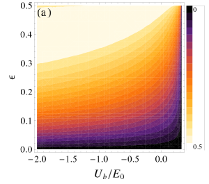
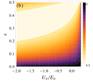
First, we focus on the spin-flip scattering taking place in the lead side. Figure 2 shows the dependence of the reflection amplitudes on for different values of with being fixed at a finite value. In the absence of the Zeeman splitting , we obtain and as expected. We numerically confirmed that this is true regardless of the polarization axis , the Rashba SOC strength , the junction parameters and . That is, no spin-flip reflection takes place when only the Rashba SOC exists. In this case the role of is to simply renormalize [see Eq. (50)] as displayed in Fig. 2(a) and (b): The perfect transmission can happen at some values of even though is used.
On the other hand, the spin-conserving feature of the reflection is no longer valid as soon as the Zeeman splitting is switched on. Figure 2(c) clearly shows that the spin-flip reflection occurs for finite values of and its amplitude, increases with . The spin-flip reflection depends sensitively on the incident energy and the polarization axis as wells as , as can be seen in Fig. 3. It modulates with the spin polarization axis in the lead, and more importantly, decreases rapidly with increasing . Although the amplitude of spin-flip scattering can be considerable close to the band bottom, , it becomes negligibly small with the incident energy well above the band bottom. It explains why the previous works (Yi1997apr, ; Frustaglia2001nov, ; Hentschel2004apr, ) could not notice the breakdown of the current conservation with their wrong -matrix: Unless the energy is close to the band bottom, the spin-flip scattering makes quite small contribution to the total current. However, its presence, though being small, is important to fulfill both the current conservation and the correct mathcing of the wave function.
Figure 4 displays the transmission amplitudes and as functions of for spin injection from the lead. In the absence of the Zeeman splitting, and hold no matter what values the other parameters have. Similar relations can be found for spin injection as wells. It is because the eigenstates and make time-reversal pairs with and , respectively. However, the introduction of finite Zeeman splitting breaks the time reversal symmetry of the system, and the balance between the transmission coefficients is gone. The transmission amplitudes for different and behave differently with increasing because the group velocities are all different and the spin overlap between the injected wave and the eigenstates also get different from each other. Note that the transmission amplitudes are not necessarily smaller than one since it is the current, not the tunneling coefficient that satisfies the unitary condition.
As proposed in our formalism, the charge current conservation, is well satisfied as shown in Fig. 5. Interestingly, the time-reversal breaking and its consequences on the transmission amplitudes do not invalidate the symmetric scattering to two arms imposed on the raw -matrix, Eq. (25). As can be seen from Fig. 5, the normalized currents in both arms are observed to always satisfy . One would guess that the imbalances in the transmission amplitudes [see Fig. 4] and non-orthogonality of the eigenstates lead to the asymmetry between the scatterings at upper and lower buffer-arm interfaces. However, our calculations show that the symmetric property of the junction remains untouched based on the fact that the raw -matrix is symmetric and the upper and lower arms are identical.
Finally, we extract the effective spin-dependent control parameters from
| (63) |
as a function of and in Fig. 6. As expected, depends sensitively on , and is spin-dependent: . Moreover, it also depends on the ring property such as the strength of Rashba SOC and Zeeman term so that in contrast to the conventional scattering theory the scattering at a junction is not determined solely by the junction itself but is affected by the arm property as wells.
IV.3 Aharonov-Bohm Interferometry
In this section we investigate the charge and spin transport through the Aharonov-Bohm type interferometer in the presence of both the Rashba SOC and Zeeman terms. We divide the study into two regimes: weak- and strong-coupling limits. In the weak-coupling regime where the effective control parameters are small, the transport features the quantized levels in the ring, while in the strong-coupling regime the interference between the eigenstates is important.
IV.3.1 Weak-Coupling Limit
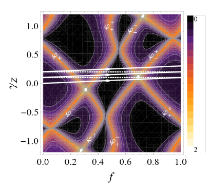
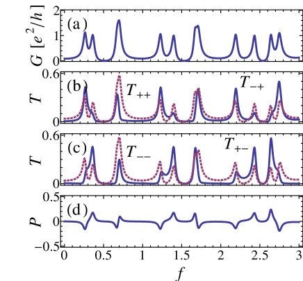
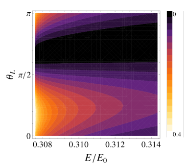
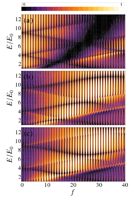
Figure 7 shows a typical dependence of the charge conductance on and in the weak-coupling limit with and . The high transmission (the bright lines) occurs when the quantization condition, Eq. (61) is satisfied. Here the resonant tunneling via the quantized ring levels boosts the transmission. This boosting is not affected by the choice of the spin polarization axis in the leads. Exactly same charge conductance is obtained by taking the spin polarization axis along the axis instead of the axis used in Fig. 7. The conductance plot is symmetric with respect to the point , which is attributed to the relations in Eq. (56). In addition, the resonance lines exhibit the anti-crossing-like behavior, which is absent in the quantized levels themselves, Eq. (61). The anti-crossing behavior originates from the Fano-like anti-resonance between two degenerate ring states whose spin polarizations are rather parallel, leading to large overlap between their wavefunctions. In this case, the injected state with any spin polarization has almost same overlaps with the degenerate ring states, resulting destructive interference between them in the transmitted state. It happens mostly when the time-reversal pair states or cross as seen in Fig. 7 and less frequently when the counter-propagating pair states or do. For the pairs or , their spin polarizations are almost orthogonal to each other so that the transport through each state is almost independent of that through the other, and their transmission amplitudes are simply additive.
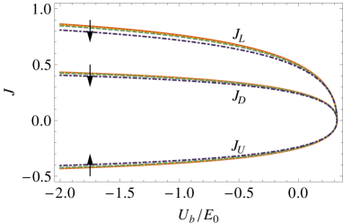
In Fig. 8(a) the charge conductance is calculated as a function of external magnetic field or the normalized flux by taking into account the linear relation, Eq. (57) between and with the ratio which is indicated by the white lines in Fig. 7. The charge conductance clearly exhibits four (or three) peaks as the magnetic flux is increased by one flux quantum . The accidental degeneracy in the ring levels enhances the conductance further, while it is still smaller than the two-channel maximum value . The fluctuations in the peak heights is mainly due to the variation of spin polarization axis of the ring eigenstates at junctions.
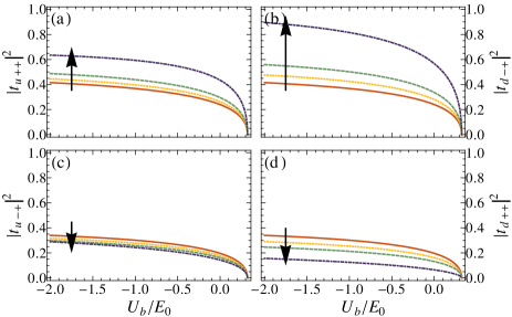
Each ring eigenstate, having the crownlike spin texture, brings about the spin-flip transport as shown in Fig. 8(b) and (c). While the peaks in the spin-flip transmission amplitudes (solid lines) are located at the same positions as those in the charge conductance, they alternate between and : the level give rise to the enhancement of and the level to that of . This level dependence is easily understood from the fact that the spin polarization of the level has inward/outward radial component. Since the tilt angle varies between 0 and , however, the spin-flip amplitudes also fluctuate. In addition, each level also makes the comparable contribution to the spin-conserving transmissions, (dotted lines), which follow the behavior of the charge conductance. These spin-dependent transmission enables the unpolarized current input to generate the spin polarized current. As seen in Fig. 8(d), the current polarization exhibits peaks and valleys whenever the spin-flip transmission is enhanced. However, since the spin blocking or the spin flip occur only partially, its magnitude is usually much smaller than 1/2.
In order to achieve the complete spin polarization or spin flip, the lead spin axis should be set to align with the (energy-dependent) spin polarization of the level at the junction. However, the arbitrary tuning of the spin polarization of the lead is not easy to implement. Instead, one can adjust the spin polarization of the ring level to the predefined spin axis of the lead by tuning the external magnetic field. The formulas for the tilt angle, Eq. (55) show that a special adjustment, yields , setting the spin polarization axis of the arm state at junctions along the direction. The adjustment requires the energy
| (64) |
(here is chosen) and the quantization condition
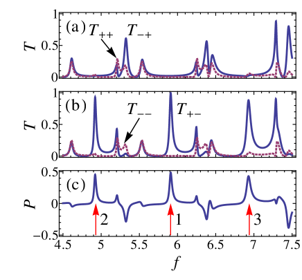
| (65) |
From Eq. (65), together with Eq. (57), the candidates for the magnetic field or the normalized Zeeman splitting are suggested, and the energy is then determined through Eq. (64). Figure 9 displays the variation of transmission amplitudes with in Eq. (65). At the point 1 , the two conditions, Eqs. (64) and (65) are exactly satisfied with so that is almost at its maximum and the other amplitudes are negligible. Hence, the conditional spin switch is embodied: the spin is completely blocked while spin is completely flipped. At the same time, the maximal current polarization shown in Fig. 9(c) indicates that it can also work as the perfect spin polarizer for unpolarized injection. The opposite spin switch that flips spin to can be implemented by reversing the direction of the external magnetic field so that the two conditions are satisfied with . Note that the behavior as the perfect spin switch or spin polarizer appears at (points 2 and 3) as wells. It is due to the small ratio used in calculations: does not change so much for a few periods of so that the conditions, Eqs. (64) and (65) are approximately satisfied at several values of .
The spin flip occurring at the junction discussed in the previous section would spoil the spin switch efficiency by inducing the tunneling to the other spin branch, and the spin tunneling cannot be determined only by the spin texture of the levels in the ring. However, we numerically confirmed that the observed spin-switch functionality is immune to the variation of and as long as the effective control parameters are small enough. In fact, the spin flip is very weak if the injection energy is well above the band bottom [see Fig. 3]. This is the case for Eq. (64) as long as is large enough. One can then safely use the usual analysis of spin transport based on the spin precession in the ring with no spin flip at junctions.
IV.3.2 Strong-Coupling Limit
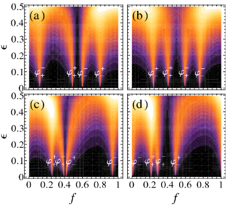
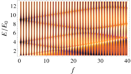
Figure 10 shows the evolution of the charge conductance as the lead-ring junction gets more transparent. The resonance feature due to the ring level, though getting smeared out with increasing , is still visible up to . For larger values of , the conductance peak position does not follow the quantization condition, Eq. (61) any longer, and instead every four consecutive peaks in a period of are merged to a single one which is located close to . In addition, a dip is formed between them. The dip appears between the time-reversal pair states if they are in succession, as can be seen in Fig. 10 (a), (c), and (d). Interestingly, the anti-crossing-like behavior can be intensified as increases as seen in Fig. 10 (c), if the pair states are close to each other in the weak-coupling limit. In this case the transparent junction enhances the destructive interference between two resonant levels. The dip can also be formed in other places if the time-reversal pair is not in succession [see Fig. 10 (b)]. In this case, the dip is less prominent, implying the destructive interference is not strong enough.
The charge transport in the strong-coupling limit , as seen in Fig. 11, clearly exhibits the well-known AB oscillations as the magnetic flux is varied. In addition, the Zeeman splitting , increasing linearly with , superposes line-shaped patterns upon the AB oscillations along which the conductance is suppressed. This suppression is due to the localization effect in the ring. To be simple, consider the Rashba-free system. The analytical expression for spin-dependent transmission amplitude is then available:
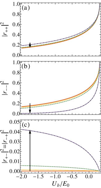
| (66) |
with given by Eq. (50), and . The transmission vanishes not only when but also when where is an integer. The latter condition means that the wave in the ring forms the standing wave so that the state is localized and does not contribute to the transport. Hence the conductance suppression happens at , making spin-dependent dark lines in the charge conductance [see Fig. 11]. The Rashba SOC, present in our system but rather small, makes a perturbative coupling between spin- and states, inducing the anti-crossing of dark lines that would be degenerate otherwise. Finally, one can notice that in the lower right corner of Fig. 11 (under the line ) the charge conductance is quite suppressed; the maximum is reduced by half, reaching , not . It is because in this region so that only the spin- channel is open. The spin- channel exists in the evanescent waves whose contribution decreases exponentially with .
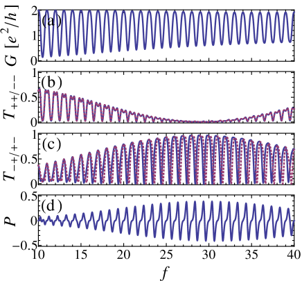
The spin transport in the strong-coupling limit is examined in Fig. 12. Similarly to the charge conductance, the spin-dependent transmissions feature the AB oscillations and the localization-induced dark line patterns. In addition, they also exhibit a global modulation of the height of the AB peaks. Interestingly, the modulation patterns are in opposite trends between spin-conserving transmissions ( and ) and spin-flip transmissions ( and ): when the spin-conserving transmissions are strong the spin-flip transmissions are weak and vice versa. This opposing behavior is clearly displayed in Fig. 13 where the charge and spin transmissions are calculated at a given injection energy, . This global modulation of spin-dependent transmission is surely related to the variation of with : is used here. Subsequently, the non-adiabatic geometric phase connected to the Rashba SOC and the Zeeman splitting varies gradually and changes the interference between the ring modes, resulting in the modulation of the spin-dependent transmission. With the total charge transmission unchanged so much, the decrease of the spin-conserving transmission then accompanies the enhancement of the spin-flip transmission. Hence, in the regime of parameters where the spin-conserving transmissions are negligible, a unconditional spin switch is implemented: the injected spin is switched to the spin and vice versa. As can be seen in Fig. 12 and Fig. 13, the parameter regime for the system to act as a good spin switch is quite wide: the working condition encloses several periods of and wide range of energy. It is attributed to the slow variation of the geometrical phase with . Finally, this system can also behavior as a good spin polarizer for unpolarized current injection, as seen in Fig. 13(d). Since the maxima of and are off the synchronization, the current polarization oscillates strongly between -0.4 and 0.4. The polarization of spin current can then be easily tuned by changing the magnetic flux by the half flux quantum .
V Discussion and Conclusion
We have proposed a general scattering-matrix formalism that naturally guarantees the charge conservation through a quantum ring with arbitrary spin-dependent interactions. To the end, we insert artificial SOC-free buffers in the vicinity of every junction and solve the system Hamiltonian in a standard way. The original problem is recovered by shrinking the size of buffers to zero, while the effect of buffers still remains. It is found that as long as the ring has nonorthogonal spin textures the spin-flip scattering can happen even if the junction itself is nonmagnetic. In the case of -type semiconductor with both the Rashba SOC and the Zeeman splitting, the finite spin-flip scattering and the conservation of charge current are numerically confirmed. In addition, it is found that the interplay of the AB and AC effects, in the presence of the Zeeman splitting, enables the ring interferometer to act as conditional/unconditional spin switch in the weak/strong coupling limit.
It should be noted that our formalism is not restricted to the structure of the AB interferometer used in this paper. The technique of inserting artificial buffers and shrinking them to zero can be applied to any network of semiconductors with arbitrary SOC. As stated above, the merit of our formalism is that the charge conservation at junctions is guaranteed as long as the interfaces between buffers and the spin-dependent regions are treated correctly.
While in our study we focus on the simplest scattering matrix by minimizing the number of physical parameters for buffers, the scattering matrix can be more generalized by introducing some spin-dependent coupling into the buffers in a controlled way. The extended form of the scattering matrix may give us a hint for the general structure of the scattering matrix connecting any spin-dependent channels with a single constraint: the charge current conservation. It would be interesting to find out the general form of the scattering-matrix based on no other than the conservation law without leaning on the specific model such as buffers.
Acknowledgements.
This work is supported by grants from the Kyung Hee University Research Fund (KHU-20090742).References
- (1) M. Büttiker, Y. Imry, and M. Y. Azbel, Phys. Rev. A 30, 1982 (1984).
- (2) D. Loss, P. Goldbart, and A. V. Balatsky, Phys. Rev. Lett. 65, 1655 (1990).
- (3) D. Loss and P. M. Goldbart, Phys. Rev. B 45, 13544 (1992).
- (4) Y.-S. Yi, T.-Z. Qian, and Z.-B. Su, Phys. Rev. B 55, 10631 (1997).
- (5) R. A. Römer and M. E. Raikh, Phys. Rev. B 62, 7045 (2000).
- (6) K. Kang and S.-C. Shin, Phys. Rev. Lett. 85, 5619 (2000).
- (7) D. Frustaglia, M. Hentschel, and K. Richter, Phys. Rev. Lett. 87, 256602 (2001).
- (8) F. E. Meijer, A. F. Morpurgo, and T. M. Klapwijk, Phys. Rev. B 66, 033107 (2002).
- (9) M. Hentschel, H. Schomerus, D. Frustaglia, and K. Richter, Phys. Rev. B 69, 155326 (2004).
- (10) D. Frustaglia and K. Richter, Phys. Rev. B 69, 235310 (2004).
- (11) X. F. Wang and P. Vasilopoulos, Phys. Rev. B 72, 165336 (2005).
- (12) M. Lee and C. Bruder, Phys. Rev. B 73, 085315 (2006).
- (13) P. Lucignano, D. Giuliano, and A. Tagliacozzo, Phys. Rev. B 76, 045324 (2007).
- (14) A. A. Kovalev, M. F. Borunda, T. Jungwirth, L. W. Molenkamp, and J. Sinova, Phys. Rev. B 76, 125307 (2007).
- (15) M. Pletyukhov and U. Zülicke, Phys. Rev. B 77, 193304 (2008).
- (16) M. F. Borunda, X. Liu, A. A. Kovalev, X.-J. Liu, T. Jungwirth, and J. Sinova, Phys. Rev. B 78, 245315 (2008).
- (17) D. Stepanenko, M. Lee, G. Burkard, and D. Loss, Phys. Rev. B 79, 235301 (2009).
- (18) C. P. Umbach, S. Washburn, R. B. Laibowitz, and R. A. Webb, Phys. Rev. B 30, 4048 (1984).
- (19) R. A. Webb, S. Washburn, C. P. Umbach, and R. B. Laibowitz, Phys. Rev. Lett. 54, 2696 (1985).
- (20) T. Bergsten, T. Kobayashi, Y. Sekine, and J. Nitta, Phys. Rev. Lett. 97, 196803 (2006).
- (21) B. Habib, E. Tutuc, and M. Shayegan, Applied Physics Letters 90, 152104 (2007).
- (22) B. Grbiĉ, R. Leturcq, T. Ihn, K. Ensslin, D. Reuter, and A. D. Wieck, Phys. Rev. Lett. 99, 176803 (2007).
- (23) F. Qu, F. Yang, J. Chen, J. Shen, Y. Ding, J. Lu, Y. Song, H. Yang, G. Liu, J. Fan, Y. Li, Z. Ji, C. Yang, and L. Lu, Phys. Rev. Lett. 107, 016802 (2011).
- (24) Y. Aharonov and D. Bohm, Phys. Rev. 115, 485 (1959).
- (25) Y. Aharonov and A. Casher, Phys. Rev. Lett. 53, 319 (1984).
- (26) S. A. Wolf, D. D. Awschalom, R. A. Buhrman, J. M. Daughton, S. von Molnár, M. L. Roukes, A. Y. Chtchelkanova, and D. M. Treger, Science 294, 1488 (2001).
- (27) I. Zutić, J. Fabian, and S. Das Sarma, Rev. Mod. Phys. 76, 323 (2004).
- (28) J. Nitta, T. Akazaki, H. Takayanagi, and T. Enoki, Phys. Rev. Lett. 78, 1335 (1997).
- (29) S. Datta, Electronic Transport in Mesoscopic Systems (Cambridge University Press, Cambridge, 1995).
- (30) The solution, Eq. (52) is valid only when the energy is larger or equal to the bottom of the upper spin branch, . Otherwise, the evanescent waves should be taken into account or all the four eigenstates belong to the lower spin branch.