Graphene Nanogap for Gate Tunable Quantum Coherent Single Molecule Electronics
Abstract
We present atomistic calculations of quantum coherent electron transport through fulleropyrrolidine terminated molecules bridging a graphene nanogap. We predict that three difficult problems in molecular electronics with single molecules may be solved by utilizing graphene contacts: (1) a back gate modulating the Fermi level in the graphene leads facilitate control of the device conductance in a transistor effect with high on/off current ratio; (2) the size mismatch between leads and molecule is avoided, in contrast to the traditional metal contacts; (3) as a consequence, distinct features in charge flow patterns throughout the device are directly detectable by scanning techniques. We show that moderate graphene edge disorder is unimportant for the transistor function.
pacs:
73.63.-b, 73.63.Rt, 85.65.+h, 72.80.VpI Introduction
The isolation of graphenenov04 has lead to a wide range of scientific discoveries and technological opportunities.Geim2007 ; Geim2009 These include, for instance, a half-integer quantum Hall effectnov2005 ; zhang2005 with potential for a drastically improved quantum resistance standard,tza2010 and a high electron mobility in this atomically thin crystal for applications in radiofrequency electronicslin2010 ; liao2010 with reduced short channel effectssch2010 or as a transparent flexible electrode.bae2010 In a wide perspective, graphene is a material with potential as a versatile and controllable bridge between the atomic and the micron scales, with unique opportunities for nanoelectronics applications. Chemistry tools may alter graphene properites either globally (for example chemical gatinglara2011 ) or locally (atoms and molecules binded to grapheneschedin2007 ; can2011 ). At the same time, modern lithographic techniques compatible with semi-conducting technology can be used to pattern graphene into devices and integrate them with conventional electronics.pal2010 Building on these discoveries, we show in this paper how graphene patterned to form a nanogap can be used as electrodes for gate-tunable molecular electronics with single molecules. The transistor effect is achieved by gating the graphene electrodes while additional device functionalities can be built into the molecule bridging the nanogap.
The idea of utilizing single molecules as active elements for electronics applications are based on a number of observations,Joa_review ; Cuniberti_book ; Bjo_review ; cuevas_book including device minituarization, reproducibility, and functionality. Besides being the ultimately small object, molecules can be mass-replicated and their functionality can be tailored through molecular synthesis. Many functional single molecule devices have been demonstrated,Tao_review but many problems remain before practical applications can be realized. Traditionally, a metal such as gold has been used to make contacts, although other configurations such as semiconducting substrates combined with the scanning tunneling microscopegui2004 ; rak2004 (STM), have been shown to work as well. The huge size mismatch between metallic leads ( nm thick) and molecules is unavoidable, which makes nanogap fabrication challenging. Utilization of the STM for contacting molecules is not a scalable technology and mainly suited for making devices for research. In addition to the problem of making nanogaps, an equally important problem for molecular electronics is how to make good molecular transistors.kub03 ; oso08 The difficulty is to put a gate sufficiently close to the molecule in a metallic nanogap to achieve a gate effect.
Here, we study theoretically the prospects of using graphene as a platform for single molecule electronics, where graphene nanostructures are used as contacts and interconnects instead of metal wires. The main purpose of this paper is to show that a transistor effect can be achieved by utilizing a back gate that changes the electron density and the density of states at the Fermi level of the graphene leads. This transistor effect works well when the coupling of the gate to the molecule is weak compared with the coupling of the gate to the leads, which is the opposite situation to a traditional molecular transistor, including nanotube-based devicesguo2006 although sharing the same robustness as these through a resonance tunneling mechanism.hyld In addition to the transistor effect, the usage of graphene, being one-atom thick, would circumvent the size-mismatch problem experienced with metal contacts.
The current fast improvements in graphene patterning and device fabrication,biro2010 ; wang10 ; he2010 have opened new opportunities for making advanced devices. These include gas sensors,schedin2007 nanopores for DNA sequencing,postma2010 ; pra2011 and single-electron transistors operated as read out devices.can2011 In the latter experiment, magnetic molecules were deposited on top of a graphene constriction. By utilizing an external magnetic field, the spin states of the molecules were manipulated, as could be read off by the graphene single-electron transistor working in its conducting state. We conclude that with this rapid progress in graphene device fabrication, the devices we shall study here can be made in the near future.
II Model
The geometry of the molecular transistor we are considering is shown in Fig. 1(a). The molecule, resembling a dumbbell, consists of a central wire of 1,4-phenylenediamine with C60 end-groups (i.e. fulleropyrrolidine terminated benzene), as depicted in Fig. 1(b). The wide graphene leads extends far from the molecule and are electrically connected to source and drain. A back gate can be used to change the position of the Dirac point in the graphene bandstructure with respect to the molecular energy levels. We describe this gate effect in more detail below.
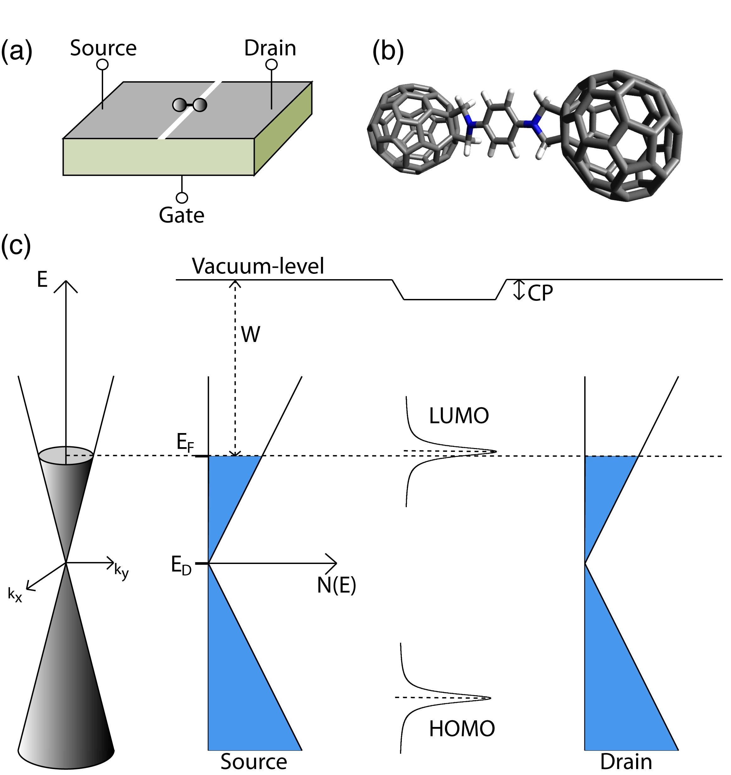
The goal of this work is not to predict the functionality of a certain molecule in great detail, or to reproduce or explain a certain experiment. Rather, the goal is to show the most salient features of a single-molecule transistor with graphene leads operating in the quantum coherent regime. But we base our studies on the specific molecule in Fig. 1. This molecule has recently attracted a lot of attention because it has promising properties for making reproducible contacts via the large C60 anchoring groups.BDC_zant ; BDC_JOC Thus, both leads and anchoring groups are made of carbon.
We shall in this work use a minimal model based on a tight-binding description. The Hamiltonian is
| (1) |
where are onsite energies, are hopping amplitudes between sites and , and the operators and create and destroy electrons on sites . We concentrate on the quantum coherent transport regime and leave effects of Coulomb interaction to future studies. This corresponds to assuming a small charging energy on the molecule compared with the molecular level broadening due to the coupling to the leads. The graphene nanostructured leads, as well as the molecule, are readily built up by restricting the sites and . We study both armchair and zigzag graphene nanoribbon leads with nearest neightbor hopping amplitude , with and without edge disorder. We include large and wide sections of the graphene leads in the calculations and connect them to ideal ribbons connected to reservoirs through the technique of self-energies. This is a Landauer approach based on non-equlibrium Green’s functions.cuevas_book ; datta_book We will for simplicity focus on the low-bias regime and present results for the transmission function of the device, as well as spectral charge current flow patterns inside the device. We note that it is important to have wide ribbons, with edge disorder on a length scale smaller than the ribbon width, otherwise weak links may form at necks of the imperfect graphene ribbon. Two such necks define a quantum dot with single-electron transistor properties,ihn2010 which leads to unwanted Coulomb blockade effects in the leads.
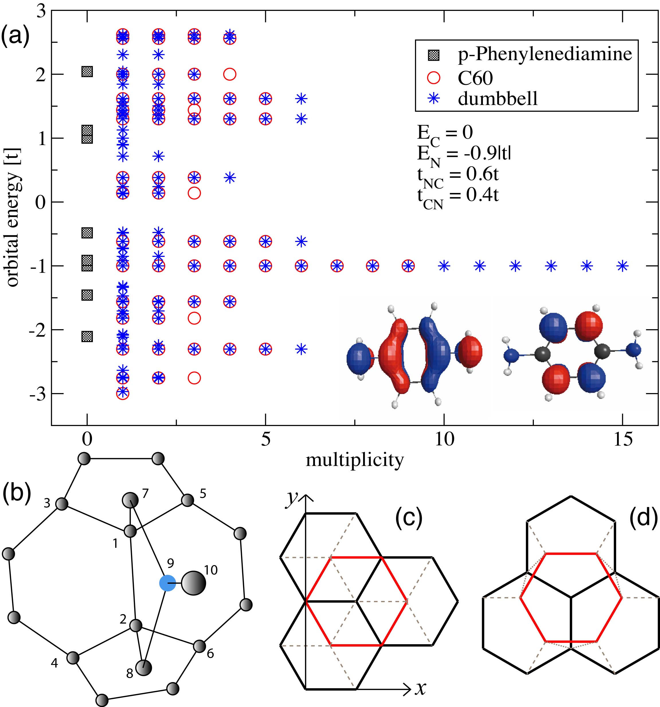
For the molecule, the C60 end groups and the benzene ring of the bridge are all carbon based, while each link group in addition contains a nitrogen atom. For our purposes, it is enough to model the molecule within the tight-binding (Hückel) theory on equal footing with the leads, and leave details to be explored in future calculations and experiments. The parameters of the molecule are kept to a minimum by only varying hopping between C60 end groups and the center phenylenediamine bridge, while letting all other carbon atoms have the same parameters in the molecule as in the graphene leads. The molecule parameters are the onsite energy on the nitrogen atom relative to the onsite energy of the carbon atoms,Inga , ( is the C-C hopping amplitude), the hopping from C60 to the nitrogen group , and the hopping from the benzene ring to the nitrogen group , see Fig. 2(b). The energy levels and orbitals of the C60 end groups are known within the tight-binding model.Dresselhaus_book For the bridge, we have compared our model with orbitals obtained with the freely available quantum chemistry package GAMESS,QC see Fig. 2(a). We would like to emphasize that if the parameters of this model are varied, unimportant details of the results may change, but the general principles of how the transistor operates will not change.
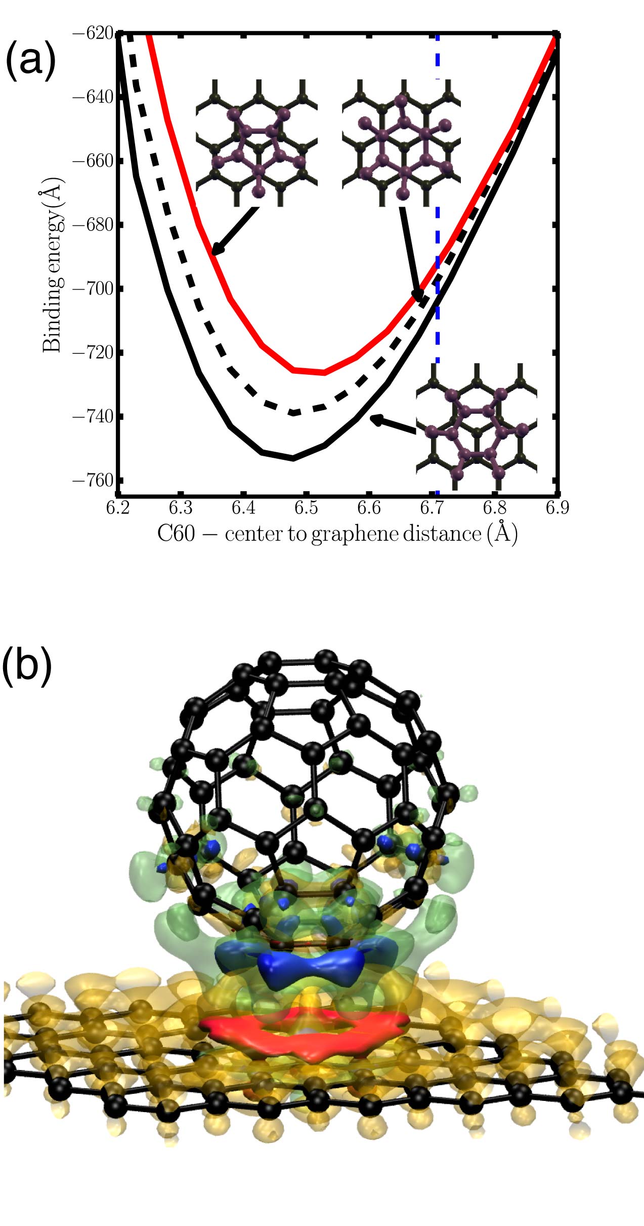
Finally, to determine the C60-on-graphene adsorption geometry and estimate both the magnitude of effective C60-graphene hopping constants and the C60-graphene charge transfer, we have performed a study using the van der Waals density functional (vdW-DF) method.dion2004 ; thon2007 The results have been obtained in a non-selfconsistent evaluation of the most recent version, vdW-DF2,lee2010 a version which some of us have previously found gives an accurate description of the binding in both a C60 crystal and of graphene layers.ber2011 We have used a plane-wave code and a standard semi-local density functional approximation, to obtain underlying results for the electron-density variation (as a function of adsorption geometries and distances). Our choice of non-selfconsistent vdW-DF evaluations is motivated by a recent analysis.thon2007
We present in Fig. 3 a summary of our vdW-DF study. Panel (a) shows vdW-DF2 results for the variation in binding energy of C60 on graphene with center-of-mass separation for three typical low-energy adsorption geometries that we have investigated in an extended search. We find that there is a systematic preference for adsorption with the C60 hexagon facing down and situated on top of a graphene atom. The panel also provides a comparison of this type of adsorption geometries (identified by the inserts which shows C60 atoms in purple, graphene atoms in black) and we find that the most favorable configuration corresponds to a 30∘ rotation of what would amont to a Bernal stacking of the hexagon on the graphene. Important for the transport modeling, we predict that the optimal adsorption separation is smaller than the value (vertical dashed line) which would corresponds to the predicted layer separation in graphite. We conclude that the effective C60-to-graphene hopping constants must be chosen larger than the choice which is made in a tight-binding modeling of graphite; in the qualitative transport modeling below, we simply set the enhancement at a factor of two. The two lowest energy configurations (solid and dashed lines in Fig. 3) corresponds, in the transport calculation below, to anchoring of the dumbbell molecule for zigzag (orientation O1) and armchair (orientation O2) leads, respectively [see Fig. 2(c)-(d)].
In Fig. 3(b) we show the details of the C60 adsorption and the complex charge transfer which we have calculated for the optimal adsorption geometry. The blue colors shows regions of electron accumulation whereas the red regions identify an electron depletion (relative to a superposition of the graphene and C60 electron densities). The panel shows that the binding is characterized not only by van der Waals forces but also by a pronounced dipole (and even multipole) formation. In addition, we findneat2006 a net charge transfer from the graphene and to the C 60. We find that the C60-on-graphene binding is beyond simple physisorption as the charge rearrangement causes a work function shift.neat2006 ; kaas2008
The first step in the transport characterization is to obtain the retarded Green’s function of the system, which is a matrix in the site indices. We utilize our own implementation of a recently developed recursive algorithmwaintal within which the sites are added one by one, which is ideal for our devices with complicated geometries. The advanced Green’s function is obtained by hermitian conjugation . Observables are related to the lesser Green’s function . In the absence of electron correlations, the expression for the lesser Green’s function is reduced to the form
It involves the distribution functions of the leads and self-energies at the surfaces of the leads that remain after eliminating the leads in favor of the system Green’s function. The leads are enumerated by the index (here and for source and drain) and surface sites of the leads are labeled by and . Local charge current flow in the device (bond current between sites and ) is written as
| (2) |
The transmission function can also be written in terms of the retarded Green’s function and self-energies of the leads,
| (3) |
where , is the propagator between leads and , and the trace is over the surface sites. Or we may compute by integrating the bond-currents [Eq. 2] flowing through an interface of the device.
III Transistor effect
In Fig. 4(a) we show an example of a transmission function for one molecule in the center of the graphene nanogap in a symmetric position, here for armchair leads. The transmission displays typical resonance features near the molecular levels of the isolated molecule. The levels are shifted and broadened by the coupling to the leads. The amount of broadening depends on the exact coupling of the molecule to the graphene, but also on the nature of the molecular orbitals. For this particular molecule, the LUMO is mainly centered on the C60 anchoring groups that act as effective extensions of the leads, while the bridge acts as the weak link in the system. Functionality can be added to the device by choosing a different bridge by exchanging the benzene ring during molecular synthesis.BDC_JOC But here we shall continue working with the benzene bridge and focus on the transistor effect.
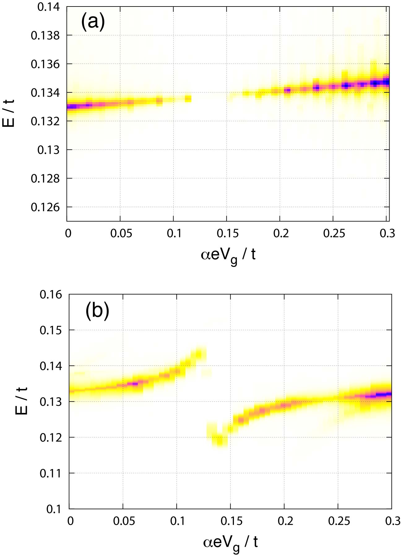
In Fig. 4(b) we present a contour plot of the transmission function for energies (vertical axis) near the LUMO as we rigidly shift the band structure of the graphene leads relative the molecular level by a back gate voltage (horizontal axis with a transfer function between the gate voltage and the shift of the Dirac point). The gate effect we have in mind can be visualized starting from Fig. 1 as moving the graphene bands vertically keeping molecular levels and the Fermi level fixed. When the Dirac point is far from the molecular level, the transmission resonance corresponds to the transistor in the on-state. As the Dirac point in the bandstructure approaches the molecular level, either from below or above in energy, the transmission resonance is shifted due to hybridization with zigzag nanogap edge states. The possibility of such hybridization was also noted recently in a DFT calculation.mot2011 . When the Dirac point passes through the level, the transmission is suppressed and the transistor is in the off-state, see Fig. 4(b) at . The on and off states will be well separated when the Dirac point can be shifted by , larger than the molecular level broadening .
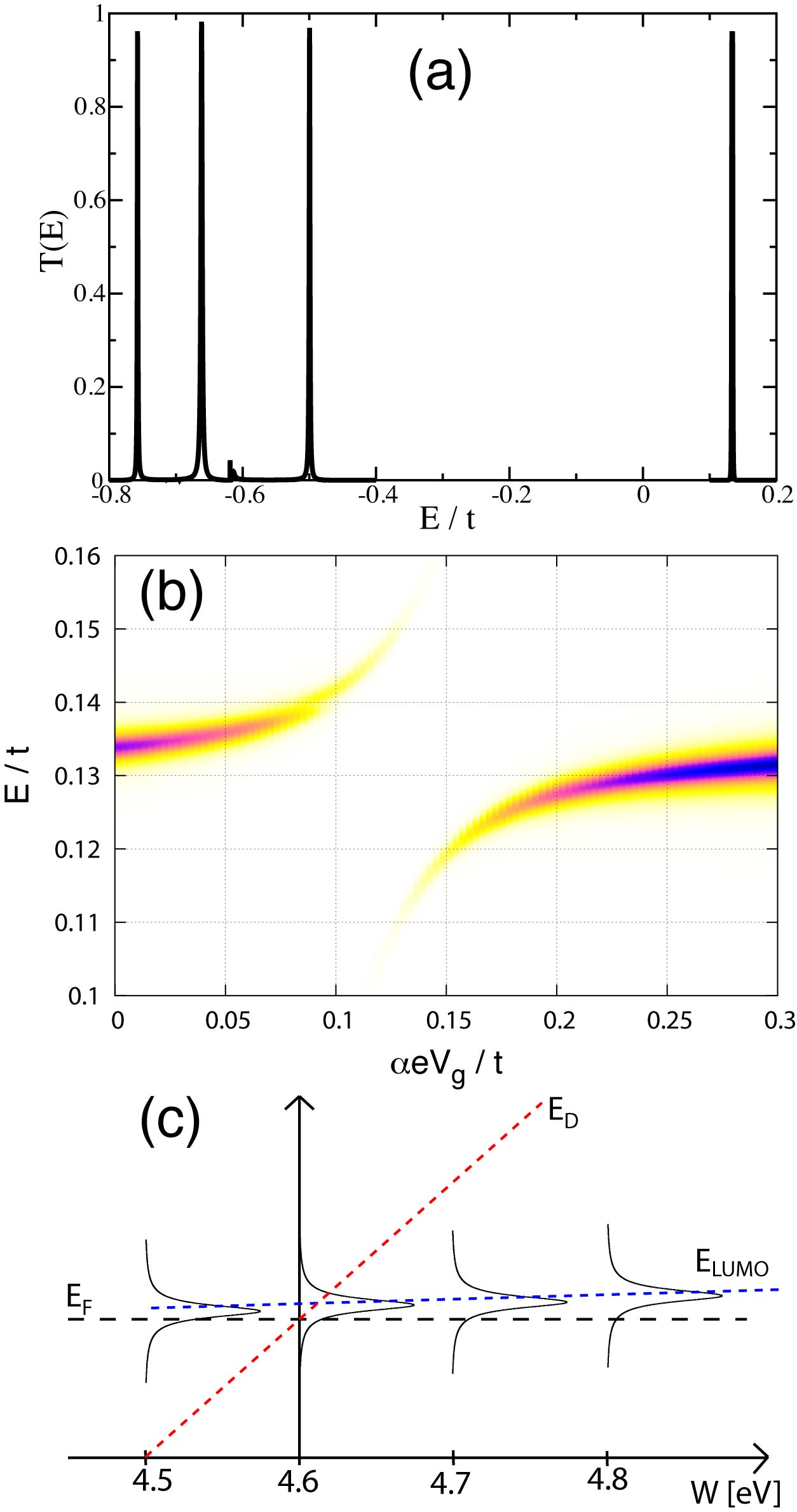
The transistor on-off ratio will be large when the Fermi level is aligned close to a molecular level. This is the case here, with in the broadened LUMO. We can estimate the molecular level alignmentDatta_Review with respect to the Fermi level by estimating the charge transfer between graphene and C60. We do that by comparing the work function of graphene with metals for which the charge transfer to C60 has been measured. It has been shown by scanning Kelvin probe microscopyYu_NL2009 that the application of a back gate voltage results in a change of the graphene work function between 4.5 eV (electron doped) and 4.8 eV (hole doped). Scanning tunneling experiments and DFT calculations of C60 on gold and silver surfaces showLu_PRB2004 that the charge transfer to C60 from gold is vanishingly small, while it is of order from silver. The work function of silver is 4.6 eV, while that of gold is 5.3 eV. This picture is corroborated by our vdW-DF study which identified a net charge transfer and dipole formation. In summary, we draw the conclusion that there is considerable charge-transfer effects already for hole-doped leads ( eV), which results in the Fermi level energy in our system aligned inside the broadened LUMO. As the gate voltage is changed, the charge transfer to the molecule will increase as we go through the Dirac (neutrality) point of graphene to the electron doped side (eventually reaching eV), which results in a Fermi level deeper inside the LUMO. Based on these estimates, where the Dirac point can be shifted by at least through the LUMO, see Fig. 4(d), the on-off ratio will be large but the precise value will ultimately have to be determined by experiment. The back gate is straightforward to use compared with the traditional direct gating of the molecule itself. In fact, the transistor effect is most effective when the gate is decoupled from the molecule and only affects the graphene leads.
In Fig. 5(a) we show the gate effect for the case of wide zigzag graphene leads, with the anchoring of the C60 end groups in orientation O1. For this orientation, there is no nanogap edge states, since the nanogap has armchair orientation. The strong hybridization of the molecular level with lead states is therefor absent and we predict a simple weak shift of the molecular level with gate voltage. As the Dirac point is tuned through the molecular level, the transmission is quenched, and we have a transistor effect analogous to the case with armchair leads discussed above.
We note that graphene itself (without nanogap and molecules as weak links) works as a transistor via the back gate. However, the graphene transistor can not be set in the off-state as the minimal conductivity is of order , in contrast to the molecular transistor with graphene leads that we study here. A nanoribbon has an energy gap related to its width, and would work as a transistor with an off-state. However, the required ribbon width is small (a few nm) and it is very difficult to control the nanopatterning with the required atomic resolution. In contrast, as we show below, the molecular graphene nano-gap transistor is more robust against edge disorder in the graphene leads.
IV Charge flow patterns
Since graphene is 100 % surface, it is an ideal material to study by scanning techniques.con2010 Previously, atoms and molecules on metal surfacesLu_PRB2004 or large-area graphenebra2011 have been studied by scanning tunneling microscopy (STM) and spectroscopy (STS) and valuable details about e.g. orbitals and charge transfer have been obtained. Scanning techniques have been utilized to reveal local information about Coulomb interactions in graphene nanostructures.schnez10 Quantum transport through quantum point contacts in 2DEGs have been mapped outTopinka_review by scanning gate spectrocsopy (SGS) and revealed so-called branched flow originating from a background random potential due to doping impurities in the layers forming the 2DEG. SGS has also been used to reveal coherent electron transport in large-area graphene flakes.ber2010a ; ber2010b Clearly, transport in a molecular device with metal electrodes is hidden by the bulky nature of the metallic contacts. Graphene on the other hand, being two-dimensional, would be a uniquely suitable electrode enabling information about quantum transport in a molecular device to be revealed by scanning techniques.
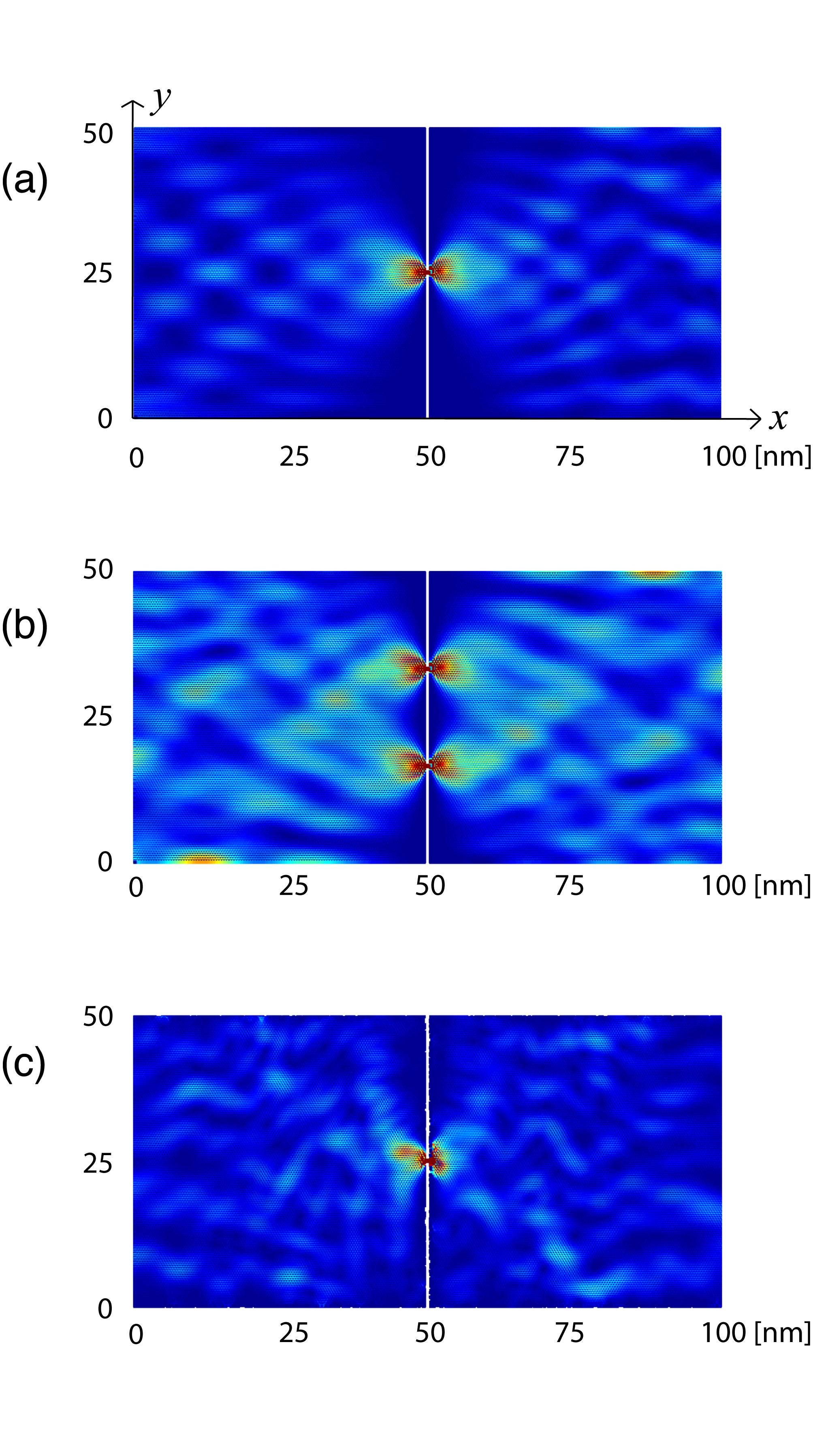
In Fig. 6(a) we present the spectral current flow pattern [the integrand in Eq. 2] through the device for an energy corresponding to the top of the LUMO peak in the transmission shown in Fig. 4(a). The position of the molecule is clearly visible in the current flow pattern. The molecule forms the weak link where all current is channeled through. The current is flowing in and out of the molecule in a characteristic lobe pattern, that is due to the specific anchoring of the C60 on graphene. Deep inside the electrodes, the current is carried throughout the width of the ribbon.
In Fig. 6(a) the molecule is in a symmetric position in the nanogap. If the molecule is in an asymmetric position, the charge flow pattern is simply displaced vertically and changes in an intuitive way (not shown) and the transmission function remains unchanged unless the molecule is very close to the upper or lower edges of the nanogap, within a few rings in the graphene leads. Similarly, if two molecules are bridging the nanogap, to a good approximation two flow patterns are simply superimposed, as we show in Fig. 6(b). We may expect quantum intereference between the two pathways (two molecules). The effect on the transmission function is weak in this example, however, unless the two molecules are very close to each other, with the anchoring groups only separated by a few rings in the graphene leads.
In a real device, perfect armchair or zigzag edges are hard to fabricate. In Fig. 6(c) we show an example of the effect of edge disorder, consisting of randomly removed carbon atoms within one ring from the original perfect edges. The interference patterns in the leads are now affected, but the molecular weak link remains clearly visible in the patterns of current flowing in to and out of the molecule. Also the transmission function is in its main features unaffected by defects in the leads, as we show in Fig. 5(b) [compare Fig. 4(b)]. Ideal graphene leads are not crucial for the transistor to function, since the weak link is the molecule.
V Summary and Conclusions
In conclusion, we have studied a single molecule device with graphene leads working in the quantum coherent transport regime. We predict a transistor effect that is pronounced when the gate coupling to the leads is much stronger than to the molecule. This opens new avenues for research of gate tunable quantum coherent molecular electronics with single molecules.
Acknowledgement
We would like to thank V. Geskin and G. Wendin for valuable discussions at various stages of this work. This work has been supported by the European Union through the projects SINGLE and ConceptGraphene, as well as SSF, the Swedish foundation for strategic research.
References
- (1) K. S. Novoselov, A. K. Geim, S. V. Morozov, D. Jiang, Y. Zhang, S. V. Dubonos, I. V. Grigorieva, and A. A. Firsov, Science 306, 666 (2004).
- (2) A. K. Geim and K. S. Novoselov, Nature Materials 6, 183 (2007).
- (3) A. K. Geim, Science 324, 1530 (2009).
- (4) K. S. Novoselov, A. K. Geim, S. V. Morozov, D. Jiang, M. I. Katsnelson, I. V. Grigorieva, S. V. Dubonos, and A. A. Firsov, Nature 438, 197 (2005).
- (5) Y. B. Zhang, Y. W. Tan, H. L. Stormer, and P. Kim, Nature 438, 201 (2005).
- (6) A. Tzalenchuk, S. Lara-Avila, A. Kalaboukhov, S. Paolillo, M. Syvä jarvi, R. Yakimova, O. Kazakova, T. J. B. M Janssen, V. Fal’ko, and S. Kubatkin, Nature Nanotech. 5, 186 (2010).
- (7) Y. M. Lin, C. Dimitrakopoulos, K. A Jenkins, D. B Farmer, H.-Y. Chiu, A. Grill, and Ph. Avouris, Science 327, 662 (2010).
- (8) L. Liao, Y.-C. Lin, M. Bao, R. Cheng, J. Bai, Y. Liu, Y. Qu, K. L. Wang, Y. Huang, and X. Duan, Nature 467, 305 (2010).
- (9) F. Schwierz, Nature Nanotech. 5, 487 (2010).
- (10) S. Bae, H. Kim, Y. Lee, X. Xu, J.-S. Park, Y. Zheng, J. Balakrishnan, T. Lei, H. R. Kim, Y. I. Song, Y.-J. Kim, K. S. Kim, B. Ozyilmaz, J.-H. Ahn, B. H. Hong, and S. Iijima, Nature Nanotech. 5, 574 (2010).
- (11) S. Lara-Avila, K. Moth-Poulsen, R. Yakimova, T. Bjørnholm, V. Fal’ko, A. Tzalenchuk, and S. Kubatkin, Adv. Mater. 23, 878 (2010).
- (12) F. Schedin, A. K. Geim, S. V. Morozov, E. W. Hill, P. Blake, M. I. Katsnelson, and K. S. Novoselov, Nature Mater. 6, 652 (2007).
- (13) A. Candini, S. Klyatskaya, M. Ruben, W. Wernsdorfer, and M. Affronte, Nano Lett. 11, 2634 (2011).
- (14) T. Palacios, A. Hsu, and H. Wang, IEEE Commun. Mag. 48, 122 (2010).
- (15) C. Joachim and M. A. Ratner, Proc. Natl. Acad. Sci. USA 102, 8801 (2005).
- (16) Introducing Molecular Electronics, G. Cuniberti, G. Fagas, and K. Richter, Editors, Springer, Berlin (2005).
- (17) K. Moth-Poulsen and T. Bjørnholm, Nature Nanotech. 4, 551 (2009).
- (18) Molecular Electronics: An Introduction to Theory And Experiment, J. C. Cuevas and E. Scheer, World Scientific, Singapore 2010.
- (19) See e.g. the review by N. J. Tao, Nature Nanotech. 1, 173 (2006).
- (20) N. P. Guisinger, M. E. Greene, R. Basu, A. S. Baluch, and M. C. Hersam, Nano Lett. 4, 55 (2004).
- (21) T. Rakshit, G.-C. Liang, A. W. Ghosh, and S. Datta, Nano Lett. 4 1803 (2004).
- (22) S. Kubatkin, A. Danilov, M. Hjort, J. Cornil, J.-L. Brédas, N. Stuhr-Hansen, P. Hedegård, and T. Bjørnholm, Nature 425, 698 (2003).
- (23) E. A Osorio, T Bjørnholm, J-M Lehn, M Ruben, and H. S. J. van der Zant, J. Phys: Condens. Matter 20, 374121 (2008).
- (24) X.F. Guo, J.P. Small, J.E. Klare, Y.L. Wang, M.S. Purewal, I.W. Tam, B.H. Hong, R. Caldwell, L.M. Huang, S. O’Brien, J.M. Yan, R. Breslow, S.J. Wind, J. Hone, P. Kim, and C. Nuckolls, Science 311, 356 (2006).
- (25) P. Hyldgaard and B. I. Lundqvist, Solid State Comm. 116, 569 (2000).
- (26) L. P. Biro and P. Lambin, Carbon 48, 2677 (2010).
- (27) H. M. Wang, Z. Zheng, Y. Y. Wang, J. J. Qiu, Z. B. Guo, Z. X. Shen, and T. Yu, Appl. Phys. Lett. 96, 023106 (2010).
- (28) Y. He, H. Dong, T. Li, C. W., W. Shao, Y. Zhang, L. Jiang, and W. Hu, Appl. Phys. Lett. 97, 133301 (2010).
- (29) H W. Ch. Postma, Nano Lett. 10, 420 (2010).
- (30) J. Prasongkit, A. Grigoriev, B. Pathak, R. Ahuja, and R. H. Scheicher, Nano Lett. 11, 1941 (2011).
- (31) C. A. Martin, D. Ding, J. Kryger Sorensen, T. Bjørnholm, J. M. van Ruitenbeek, and H. S. J. van der Zant, J. Am. Chem. Soc. 130, 13198 (2008).
- (32) J. Kryger Sørensen, J. Fock, A. Holmen Pedersen, A. B. Petersen, K. Jennum, K. Bechgaard, K. Kilsa, V. Geskin, Jerome Cornil, T. Bjørnholm, and M. Brøndsted Nielsen, J. Org. Chem. 76, 245 (2011).
- (33) Electron Transport in Mesoscopic Systems, S. Datta, Cambridge University Press, Cambridge (1995).
- (34) T. Ihn, J. Gü ttinger, F. Molitor, S. Schnez, E. Schurtenberger, A. Jacobsen, S. Hellmü ller, T. Frey, S. Drö scher, C. Stampfer, and K. Ensslin, Mater Today 13, 44 (2010).
- (35) I. Fischer-Hjalmars, Arkiv för fysik, Bd 21 nr 11, p.123 (1961).
- (36) Science of Fullerenes and Carbon Nanotubes: Their Properties and Applications, M. S. Dresselhaus, G. Dresselhaus, and P. C. Eklund, Academic Press, San Diego (1996).
- (37) M.W. Schmidt, K.K. Baldridge, J.A. Boatz, S.T. Elbert, M.S. Gordon, J.H. Jensen, S. Koseki, N. Matsunaga, K.A. Nguyen, S.J. Su, T.L. Windus, M. Dupuis, and J.A. Montgomery, J. Comput. Chem. 14, 1347 (1993). Available from: ¡http://www.msg.ameslab.gov¿.
- (38) M. Dion, H. Rydberg, E. Schröder, B.I. Lundqvist, and D.C. Langreth, Physical Review Letters 92, 246401 (2004).
- (39) T. Thonhauser, V. R. Cooper, S. Li,1 A. Puzder, Per Hyldgaard, and D. C. Langreth, Phys. Rev. B 76, 125112 (2007).
- (40) K. Lee, E. D. Murray, L. Kong, B. I. Lundqvist, and D. C. Langreth, Phys. Rev. B 82, 081101(R) (2010).
- (41) K. Berland, Ø. Borck, and P. Hyldgaard, Comp. Phys. Commun. 182, 1800 (2011).
- (42) J. B. Neaton, M. S. Hybertsen, and S. G. Louie, Phys. Rev. Lett. 97, 216405 (2006).
- (43) K. Kaasbjerg and K. Flensberg, Nano Lett. 8, 3809 (2008)
- (44) K. Kazymyrenko and X. Waintal, Phys. Rev. B 77, 115119 (2008).
- (45) C. Motta, M. I. Trioni, G. P. Brivio, and K. L. Sebastian, arXiv:1106.4965.
- (46) Electrical Conduction through Molecules, F. Zahid, M. Paulsson, and S. Datta, in Advanced Semiconductors and Organic Nano-Techniques, edited by H. Morkoc, Academic Press 2003.
- (47) Y.-J. Yu, Y. Zhao, S. Ryu, L. E. Brus, K. S. Kim, and P. Kim, Nano Lett. 9, 3430 (2009).
- (48) X. Lu, M. Grobis, K. H. Khoo, S. G. Louie, and M. F. Crommie, Phys. Rev. B 70, 115418 (2004).
- (49) M. R Connolly and C. G Smith, Phil. Trans. R. Soc. A 368, 5379 (2010).
- (50) V. W. Brar, R. Decker, H.-M. Solowan, Y. Wang, L. Maserati, K. T. Chan, H. Lee, C. O. Girit, A. Zettl, S. G. Louie, M. L. Cohen, and M. F. Crommie, Nature Phys. 7, 43 (2011).
- (51) S. Schnez, J. Güttinger, M. Huefner, C. Stampfer, K. Ensslin, and T. Ihn, Phys. Rev. B 82, 165445 (2010).
- (52) M. A. Topinka, R. M. Westervelt, and E. J. Heller, Physics Today vol. 56 (12), 47 (2003).
- (53) J. Berezovsky, M. F. Borunda, E. J. Heller, R. M. Westervelt, Nanotechnology 21, 274013 (2010).
- (54) J. Berezovsky and R. M. Westervelt, Nanotechnology 21, 274014 (2010.