Common Origin of the Circular-dichroism Pattern in ARPES of SrTiO3 and CuxBi2Se3
Abstract
Circular dichroism in the angular distribution (CDAD) of photoelectrons from SrTiO3:Nb and CuxBi2Se3 is investigated by 7-eV laser ARPES. In addition to the well-known node that occurs in CDAD when the incidence plane matches the mirror plane of the crystal, we show that another type of node occurs when the mirror plane of the crystal is vertical to the incidence plane and the electronic state is two dimensional. The flower-shaped CDAD’s occurring around the Fermi level of SrTiO3:Nb and around the Dirac point of CuxBi2Se3 are explained on equal footings. We point out that the penetration depth of the topological states of CuxBi2Se3 depends on momentum.
The interaction of light with matter depends on the polarization of the photons. Circular dichroism (CD) is a phenomenon in which the response of a system to left and right circularly polarized light is different. CD can be microscopically attributed to the difference in the material’s response against opposite helicities of the photons. Thus, CD has been actively used for studying magnetic materials or those having strong spin-orbit interactions Thole ; Carra ; Kuch_01 . Alternatively, left and right circular polarizations are exchanged by a mirror operation, and therefore CD is active when the measurement breaks symmetry with respect to the reflection; i.e., CD occurs when the experimental geometry has “handedness” Dubs ; Schonhense_90 .
In angle resolved photoemission spectroscopy (ARPES), light is shined on a crystal and the energy-and-angle distribution of the photoelectrons is recorded. The band structures of crystals and crystal surfaces are traced by ARPES, and the information is further enriched by investigating the CD in the angular distribution (CDAD) of the photoelectrons Dubs ; Schonhense_90 ; Kuch_01 ; Suga ; Kaminski ; Borisenko ; Mattia_Ni111 ; Panaccione ; Zabolotnyy ; YbRh2Si2 . For example, a node in CDAD occurs when the incidence plane and the mirror plane of the crystal are matched Schonhense_90 . This vertical node, which occurs due to reasons of symmetry, has been utilized in various ARPES studies Kaminski ; Borisenko ; Mattia_Ni111 ; Panaccione ; Zabolotnyy ; YbRh2Si2 . In this Letter, we show that there is another type of node, a horizontal node, which occurs due to a combination of the symmetry and dimensionality of the initial electronic state. We first investigate photoemission matrix elements and derive the condition for the occurrence of the horizontal node. Then we introduce and derive information from the horizontal nodes occurring in the CDADs of SrTiO3:Nb and CuxBi2Se3.
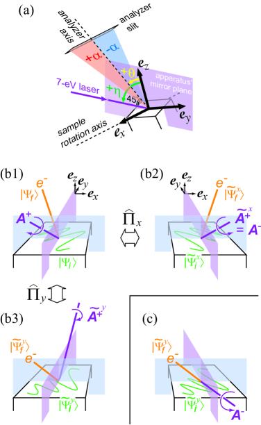
The experimental geometry of 7-eV laser ARPES Kiss is shown in Fig. 1(a). By using an orthogonal basis fixed on the sample (we take along the sample rotation axis and along the sample surface), the vector potentials for right () and left () circular polarizations are described as , where , is the angle between the laser beam and , and is a phase. The analyzer collects photoelectrons emitted within the acceptance angle ( is the direction to the analyzer axis), and the photoelectron distribution () is recorded as functions of , , and , where is the rotation angle of with respect to the analyzer axis and is the binding energy referenced to of gold. The spectra are recorded at 10 K with an energy resolution of 3 meV.

In general, a photoemission event from a given initial-to-final state ( to ) under a given experimental setup has the same cross section to another event which is a mirror reflection of the original one 93_Venus_CoreMCD . Here, everything should be reflected, not just the crystal and the incident light, but also into , and even the direction of the circulating currents responsible for magnetism, if any. We consider a one-step photoemission process, so that is an inverse low-energy electron diffraction (LEED) state extending from the sample into the detector Schonhense_90 and evaluate the operator under a dipole approximation: .
When the incidence plane matches the mirror plane of the crystal, the result obtained in a reflected experiment with respect to the incidence plane (this coincides with the apparatus’ mirror plane in our experimental geometry) is the same as that of the original experiment with a reversed circular polarization , as can be seen by comparing Figs. 1(b1) and 1(b2). One can confirm [the left- and right-hand sides of this equation correspond to the events shown in Fig. 1(b1) and 1(b2), respectively] with the aid of . Therefore , so that the angular distribution of the dichroism acquires a vertical node, i.e., .
Next, we consider a case where the mirror plane of the crystal is vertical to the incidence plane, and ask whether
| (1) |
can hold. This corresponds to investigating whether the matrix elements for the events shown in Figs. 1(b1) and 1(c) can be equivalent or not. The incidence angles are different, since the laser and the analyzer are fixed in space; thus, these two photoemission events cannot overlap by any symmetry operations. Therefore Eq. (1) does not hold globally. Nevertheless, the events shown in Figs. 1(b3) and 1(c) [the former is a reflection of Fig. 1(b1) with respect to the mirror plane, and hence, equivalent to the event of Fig. 1(b1)] resemble each other: In both cases, the initial and final states are the same, and the in-plane () components of rotate anticlockwise on the sample surface. Explicitly, Eq. (1) is equivalent to
| (5) | |||||
| (9) | |||||
and the main difference occurs in the sign (phase) of the component of the vector potential with respect to the and components. Thus, when
| (10) |
is fullfilled, Eq. (9) and, hence Eq. (1) holds at , resulting in a horizontal node = 0.

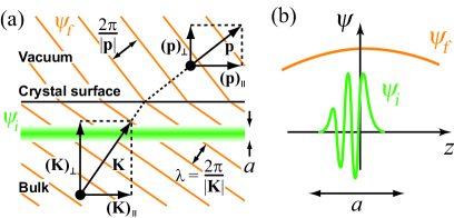
The condition (10) is fulfilled when is two-dimensional (2D) and spatially confined in the direction within a length scale shorter than the de Broglie wave length of the photoelectron final state, as shown in Fig. 2. Then, , so that the photoemission matrix element becomes susceptible only to the in-plane component of the vector potential. The small photoelectron kinetic energy achieved by the 7-eV laser is favorable for satisfying condition (10), since . Even when becomes comparable to , is usually an oscillating function for , and, therefore, the matrix element has little dependence on the component.

The case for SrTiO3:Nb.— SrTiO3 is an oxide semiconductor having a cubic perovskite structure. The bulk can be doped with carriers by incorporating Nb. Recently, it has been revealed that an inversion layer occurs at the surface of semiconducting SrTiO3 independent of the carrier concentration of the bulk Syro ; Non .
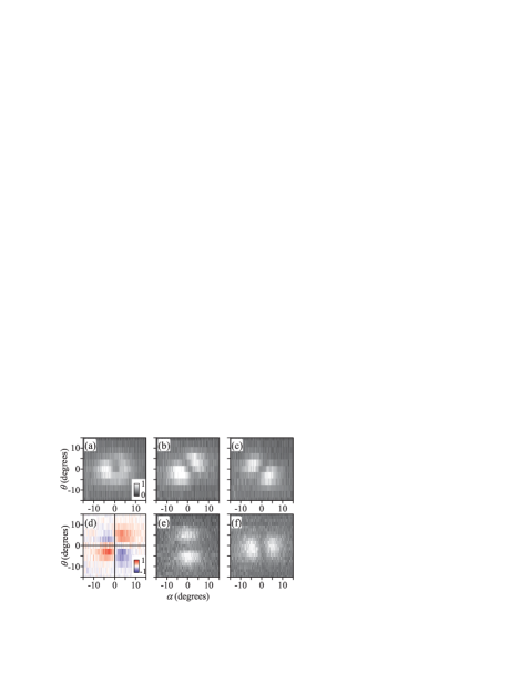
We find that the 2D electron gas formed in the inversion layer of SrTiO3 is an ideal case that exhibits the horizontal and vertical nodes. In Fig. 3, we show the angular distribution of the spectral weight near recorded on a (001) surface of 1%-Nb-doped SrTiO3 annealed in vacuum for 40 min at 550∘C. Here, [100] and [010] are aligned to and , respectively, within 5∘. A circular Fermi surface can be observed in the mapping (a), and (b) appears to be a reflection of (c) about both the and axes. Therefore, horizontal and vertical nodes occur in (d). The vertical node can be understood as a result of the (100) mirror plane matching the incidence plane, and the horizontal node can be understood from the facts that the (010) mirror plane is vertical to the incidence plane and the electronic state is 2D. The normalized dichroic asymmetry is a maximum (60 %) around . The spectral weight mapped by () polarization is bright (dark) at and dark (bright) at [see Figs. 3(e) and 3(f)], indicating that the states probed by the 7-eV laser consist of orbitals having odd parity with respect to the reflection at the and planes Cuprates_RMP ; Syro ; Non . The in-plane orbital character of the initial states may further facilitate the condition of the 2D confinement to be fulfilled.

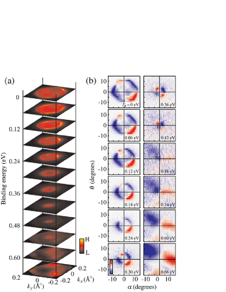
The case for CuxBi2Se3.— Bi2Se3 is found to be a topological insulator FuKaneMele_PRL ; Hasan_Rev supporting a single Dirac-cone dispersion on its surface SCZhang_NPhys ; Xia_BiSe_NPhys ; Hsieh_Tunable_Spin . Cu intercalation effectively dopes the system with electron carriers Hor_CuBiSe ; Wray_NPhys . In the present case, the nominal Cu concentration is , and is located 480 meV above , as shown in Fig. 4(a). The band dispersion in the plane ( is set along - and is parallel to within 3∘) changes from nearly isotropic to hexagonal in going away from . This can be explained within a 2D Hamiltonian constrained under and time-reversal symmetry Fu_hexagon_PRL ; Kuroda_Hexagon :
| (11) |
Here, is responsible for the hexagonal warping, is the Pauli matrix, , contains a -order correction, and introduces particle-hole asymmetry. The three-fold pattern observed in the mappings at 0.54 eV originates from the bulk valence band, and the faint intensity observed inside the hexagon near is due to the bulk conduction band Wray_NPhys .
In Fig. 4(b), we show at various ’s. In the vicinity of (at = 0.42 and 0.36 eV), we observe nodal lines at and . This can be explained by noting that the effective Hamiltonian [Eq. (11)] up to second order in is invariant under mirror operations at the and planes, and the states therein are 2D, so that the conditions for the horizontal and the vertical nodes are fulfilled. Note that it is the effective Hamiltonian, not the crystal surface, that has the mirror symmetry about the plane. On the other hand, in the bulk valence-band region at eV does not show the vertical node since the crystal does not have a vertical mirror plane. It also does not show the horizontal node since the valence-band electronic structure is three-dimensional, even though the crystal has a horizontal mirror plane at .
It is apparent that the horizontal node in the topological state is gradually distorted in going from to , even though the crystal as well as the effective Hamiltonian has horizontal mirror symmetry. This indicates that the topological states lose the condition of 2D confinement at large , and around , they penetrate deep into the bulk rather than being surface states localized on surface layers. This is supported by calculations NJP2010 and is reminiscent of a surface-state-to-surface-resonance transition with varying observed in the states on metal surface Al100 . The results thus indicate that the effective Hamiltonian Eq. (11) is valid only in the vicinity of . The deviation from Eq. (11) may be important to understand the possibly exotic superconductivity of CuxBi2Se3 Hor_CuBiSe ; Wray_NPhys ; Ando_PRL2011 ; FuBerg and the recent observation of the topological states away from acquiring out-of-plane spin components Souma .
In summary, we find that the CDADs of both SrTiO3:Nb around and Cu-doped Bi2Se3 around exhibit a flower-shaped pattern having horizontal and vertical nodes. The vertical node is explained within a well-known geometric effect Schonhense_90 , whereas the horizontal node can be understood by using a combination of the geometry and the 2D character of the initial electronic state. The length scale of the 2D confinement of the initial state is set by the de Broglie wavelength of the photoelectron final state. The horizontal node in CDADs can therefore be a measure of the two-dimensionality of the electronic states, providing information of the penetration depth of surface states and insights into the 2D electron gas formed on semiconductor surfaces.
This research is supported by JSPS through its FIRST Program. H.Y.H. and C.B. acknowledge support by the Department of Energy, Office of Basic Energy Sciences, Division of Materials Sciences and Engineering, under contract DE-AC02-76SF00515.
References
- (1) B. T. Thole, P. Carra, F. Sette, and G. van der Laan, Phys. Rev. Lett. 68, 1943 (1992).
- (2) P. Carra, B. T. Thole, M. Altarelli, and X. Wang, Phys. Rev. Lett. 70, 694 (1993).
- (3) W. Kuch and C. M. Schneider, Rep. Prog. Phys. 64, 147 (2001).
- (4) R. L. Dubs, S. N. Dixit, and V. McKoy, Phys. Rev. Lett. 54, 1249 (1985).
- (5) G. Schonhense, Phys. Scr. T31, 255 (1990).
- (6) T. Matsushita, S. Imada, H. Daimon, T. Okuda, K. Yamaguchi, H. Miyagi, and S. Suga, Phys. Rev. B 56, 7687 (1997).
- (7) A. Kaminski, S. Rosenkranz, H. M. Fretwell, J. C. Campuzano, Z. Li, H. Raffy, W. G. Cullen, H. You, C. G. Olsonk, C. M. Varma, and H. Hochst, Nature 416, 610 (2002).
- (8) S. V. Borisenko, A. A. Kordyuk, A. Koitzsch, T. K. Kim, K. A. Nenkov, M. Knupfer, J. Fink, C. Grazioli, S. Turchini, and H. Berger, Phys. Rev. Lett. 92, 207001 (2004).
- (9) M. Mulazzi, M. Hochstrasser, M. Corso, I. Vobornik, J. Fujii, J. Osterwalder, J. Henk, and G. Rossi, Phys. Rev. B 74, 035118 (2006).
- (10) F. Vidal, M. Marangolo, P. Torelli, M. Eddrief, M. Mulazzi, and G. Panaccione, Phys. Rev. B 76, 081302(R) (2007).
- (11) V. B. Zabolotnyy, S. V. Borisenko, A. A. Kordyuk, D. S. Inosov, A. Koitzsch, J. Geck, J. Fink, M. Knupfer, B. Buchner, S.-L. Drechsler, V. Hinkov, B. Keimer, and L. Patthey, Phys. Rev. B 76, 024502 (2007).
- (12) D. V. Vyalikh, S. Danzenbacher, A. N. Yaresko, M. Holder, Y. Kucherenko, C. Laubschat, C. Krellner, Z. Hossain, C. Geibel, M. Shi, L. Patthey, and S. L. Molodtsov, Phys. Rev. Lett 100, 056402 (2008).
- (13) T. Kiss, T. Shimojima, K. Ishizaka, A. Chainani, T. Togashi, T. Kanai, X.-Y. Wang, C.-T. Chen, S. Watanabe, and S. Shin, Rev. Sci. Instrum. 79, 023106 (2008).
- (14) D. Venus, Phys. Rev. B 48, 6144 (1993).
- (15) A. F. Santander-Syro et al., Nature 469, 189 (2011).
- (16) W. Meevasana, P. D. C. King, R. H. He, S.-K. Mo, M. Hashimoto, A. Tamai, P. Songsiriritthigul, F. Baumberger, and Z.-X. Shen, Nature Mater. 10, 114 (2011).
- (17) A. Damascelli, Z. Hussain, and Z.-X. Shen, Rev. Mod. Phys. 75, 473 (2003).
- (18) L. Fu, C. L. Kane, and E. J. Mele, Phys. Rev. Lett. 98, 106803 (2007).
- (19) M. Z. Hasan and C. L. Kane, Rev. Mod. Phys. 82, 3045 (2010).
- (20) H.-J. Zhang, C.-X. Liu, X.-L. Qi, X. Dai, Z. Fang, and S.-C. Zhang, Nature Phys. 5, 438 (2009).
- (21) Y. Xia, D. Qian, D. Hsieh, L. Wray, A. Pal, H. Lin, A. Bansil, D. Grauer, Y. S. Hor, R. J. Cava, and M. Z. Hasan, Nature Phys. 5, 398 (2009).
- (22) D. Hsieh et al., Nature 460, 1101 (2009).
- (23) Y. S. Hor, A. J. Williams, J. G. Checkelsky, P. Roushan, J. Seo, Q. Xu, H. W. Zandbergen, A. Yazdani, N. P. Ong, and R. J. Cava, Phys. Rev. Lett. 104, 057001 (2010).
- (24) L. A. Wray, S.-Y. Xu, Y. Xia, Y. S. Hor, D. Qian, A. V. Fedorov, H. Lin, A. Bansil, R. J. Cava, and M. Z. Hasan, Nature Phys. 6, 855 (2010).
- (25) L. Fu, Phys. Rev. Lett. 103, 266801 (2009).
- (26) K. Kuroda et al., Phys. Rev. Lett. 105, 076802 (2010).
- (27) W. Zhang, R. Yu, H.-J. Zhang, X. Dai, and Z. Fang, New J. Phys 12, 065013 (2010).
- (28) P. O. Gartland and B. J. Slagsvold, Solid State Commun. 25, 489 (1978).
- (29) M. Kriener, K. Segawa, Z. Ren, S. Sasaki, and Y. Ando, Phys. Rev. Lett. 106, 127004 (2011).
- (30) L. Fu and E. Berg, Phys. Rev. Lett. 105, 097001 (2010).
- (31) S. Souma, K. Kosaka, T. Sato, M. Komatsu, A. Takayama, T. Takahashi, M. Kriener, K. Segawa, and Y. Ando, Phys. Rev. Lett. 106, 216803 (2011).