Modeling of the transient interstitial diffusion of implanted atoms during low-temperature annealing of silicon substrates
Abstract
It has been shown that many of the phenomena related to the formation of “tails” in the low-concentration region of ion-implanted impurity distribution are due to the anomalous diffusion of nonequilibrium impurity interstitials. These phenomena include boron implantation in preamorphized silicon, a “hot” implantation of indium ions, annealing of ion-implanted layers et cetera. In particular, to verify this microscopic mechanism, a simulation of boron redistribution during low-temperature annealing of ion-implanted layers has been carried out under different conditions of transient enhanced diffusion suppression. Due to the good agreement with the experimental data, the values of the average migration length of nonequilibrium impurity interstitials have been obtained. It has been shown that for boron implanted into a silicon layer preamorphized by germanium ions the average migration length of impurity interstitials at the annealing temperature of 800 ∘C can be reduced from 11 nm to approximately 6 nm due to additional implantation of nitrogen. The further shortening of the average migration length is observed if the processing temperature is reduced to 750 ∘C. It is also found that for implantation of ions into silicon crystal, the value of the average migration length of boron interstitials is equal to 7.2 nm for thermal treatment at a temperature of 800 ∘C.
pacs:
61.72.Ji, 61.72.Tt, 61.72.Ss, 85.40.RyI Introduction
It is well known that boron is a basic impurity of p-conductivity used in the technology of the production of silicon integrated microcircuits Salvador-10 . Unfortunately, boron atoms have a small mass and large mobility in silicon crystals. Due to the small masses of boron ions, the formation of an amorphous layer in the ion-implanted substrates is not observed even at large fluencies. Only a great number of radiation defects are created. The absence of an amorphous layer and the presence of radiation defects result in the significant transient enhanced diffusion (TED) of ion-implanted boron during the subsequent annealing (see, for example, Hofker-75 ; Michel-87 ; Fan-87 ; Michel-1987 ; Eaglesham-94 ; Stolk-97 ; Lerch-99 ; Ohuchi-01 ; Mirabella-02 ; Jain-02 ; Shao-03 ; Lerch-05 ; Graoui-05 ; Gable-05 ; Lallement-05 ; Bazizi-10 ; Woon-10 ; Philippe-11 ; Shimizu-11 ). All these phenomena substantially complicate the problem of the formation of very shallow junctions with high electrophysical parameters. For suppressing the TED of ion-implanted boron, a method of boron implantation in a silicon layer preamorphized by heavier germanium ions is widely used Ohuchi-01 ; Lerch-05 ; Graoui-05 ; Gable-05 ; Mirabella-04 ; Camillo-Castillo-2004 ; Cristiano-04 ; Hopstaken-04 ; Pawlak-04 ; Pawlak-004 ; Pawlak-2004 ; Camillo-Castillo-04 ; Tomita-04 ; Lindsay-04 ; Hamilton-07 ; Ferri-07 ; Yeong-08 . Due to the solid phase epitaxial regrowth (SPER) of the amorphous layer, the region doped with boron is characterized by a perfect crystal structure, containing defects that are invisible by electron microscopy. However, the transient enhanced diffusion is observed as before, although it has another character and a smaller intensity. In the papers Velichko-10 ; Velichko-11 a qualitative difference of the form of boron profiles produced by annealing at temperatures of 800 ∘C and below was pointed out in comparison with the annealing at 900 ∘C and higher temperatures. Really, at low annealing temperatures an extended “tail” is observed in the low-concentration region of the impurity profile and the shape of this “tail” is a straight line if the axis of concentration is logarithmic. This feature of the boron distribution is observed even for “tail” extension compared to the characteristic size of the implanted region or smaller than it. At the same time, after annealing at a temperature of 900 ∘C or higher the shape of the boron profile for concentrations below approximately 108 m-3 becomes convex upwards, i.e., similar to the Gaussian distribution. This behavior of the profile shape gives clear evidence of the change in the boron diffusion mechanism.
It is worth noting that the “tails” that represent a straight line, if the axis of concentration is logarithmic, are often observed directly after ion implantation of boron, phosphorus, gallium, and other impurity at room temperature (see, for example, Hofker-75 ; Tomita-04 in the case of implantation of boron ions, Moline-71 ; Blood-74 for phosphorus implantation, Crowder-71 ; Dearnaley-75 in the case of implantation of gallium ions). The ion implantation in all the cases investigated was carried out in the direction deflecting from the crystal axis. According to Ryssel-78 , to completely remove the phenomenon of channeling and to eliminate the “tails” related to the scattering of ions into channels, the ion implantation should be carried out in amorphous silicon. Nevertheless, later experiments show that “tails” are observed for boron implantation in the layers preamorphized by germanium ions Cristiano-04 ; Hamilton-07 .
For the low-temperature treatments of ion-implanted layers either an increase and broadening of existing “tails” in the bulk of a semiconductor occur or the formation of new “tails” if they are not observed after implantation. In the region of low impurity concentration, a “tail” represents as before a straight line for low-temperature annealing (i.e. for a small thermal budget). Really, an increase in the “tail” extension occurs during subsequent thermal treatments of preamorphized silicon layers that were implanted with boron ions Cristiano-04 ; Pawlak-2004 ; Hamilton-07 ; Ferri-07 . In the investigations carried out by Gable-05 ; Camillo-Castillo-2004 ; Camillo-Castillo-04 ; Yeong-08 clearly identified “tails” after boron implantation were not observed. However, such “tails” were formed in the course of the subsequent annealing. As follows from the experimental data of Gamo-73 , a “tail” is also formed in the case of thermal treatment at 900 ∘C of silicon layers implanted with indium. This “tail” represents a straight line if the concentration axis is logarithmic. The experimental data also show that “tails” characterized by a straight line are often observed for the “hot” ion implantation of indium Gamo-73 , gallium Gamo-73 , antimony Gamo-70 , and other impurities.
It was assumed originally that the formation of “tails” in the low-concentration region of ion-implanted impurity profiles, especially in the case of “hot” ion implantation, results from the fast diffusion of implanted impurity atoms Crowder-71 ; Gamo-73 ; Gamo-70 ; Davies-68 . It was supposed that impurity interstitials are this fast diffusing species Gamo-73 ; Crowder-71 ; Davies-68 . For example, it was shown experimentally in Davies-68 that during annealing of ion-implanted layers a significant fraction of indium and tellurium atoms leave their substitutional positions and become interstitials. The interstitial position is also a characteristic feature for atoms of gallium that, as well as boron, indium, and tellurium is the element of III groups. However, in the latest papers Blood-74 ; Dearnaley-75 there are very serious arguments that the formation of “tails” in ion-implanted layers is related to the scattering of ions that reserved a part of the kinetic energy into channels. For example, in the paper Blood-74 phosphorus ions were implanted into thin silicon layers of different thicknesses. These layers were located on a substrate, which collected ions channeling through the layer. It was assumed that diffusing atoms do not have sufficient energy to leave the silicon crystal, whereas the channeling ions have. Experiments showed that the substrate really collects ions passed through the silicon layer. The doses of the passed ions were obtained as a function of the layer thicknesses. These doses correspond to the doses of phosphorus atoms in the region of the remainder of the “tail” for the investigated depth if ions were implanted in the continuous silicon. The results obtained were generalized in Dearnaley-75 for the cases of indium and gallium implantation. According to Dearnaley-75 the radiation-enhanced diffusion of gallium is impossible at room temperature. On the other hand, a characteristic “tail” is observed experimentally due to the scattering of ions into channels. Taking into account the possible annealing of damages and recovery of the crystal structure in the region of the end of the ion range, one can explain the results of Gamo-73 for “hot” high fluence implantation of indium and gallium ions without attracting the concept of an anomalous diffusion. Besides, at low temperatures a “tail” can be formed as a result of the channeling of a part of impurity atoms at the initial stage of implantation, when the amorphous phase was not formed as yet. Nevertheless, the mechanism of the “tail” formation is not clear until now, especially taking into account the latest experiments Cristiano-04 ; Hamilton-07 related to boron implantation in the layer preamorphized by implantation of germanium ions. This allows us to formulate the following purpose of the research.
II Main goal of the research
Not rejecting the possibility for a part of the ions of scattering into channels, we are to show that the long-range migration of nonequilibrium impurity interstitials is the main factor in the formation of “tails” in the region of low impurity concentration for random ion implantation into silicon crystals and implantation into preamorphized silicon layers.
III Analysis of the mechanisms of the “tail” formation during ion implantation
Let us consider four characteristic cases of the formation of “tails” in the region of impurity concentration decreasing in the bulk of the semiconductor:
(i) “Tail” formation during the subsequent annealing of ion-implanted layers Gamo-73 ; Gable-05 ; Camillo-Castillo-2004 ; Camillo-Castillo-04 ; Yeong-08 ;
(ii) Formation of “tails” during ion implantation into amorphous silicon Cristiano-04 ; Hamilton-07 ;
(iv) Formation of “tails” during ion implantation in the direction deflecting from the axis of the crystal at room temperature of the substrate Hofker-75 ; Tomita-04 ; Moline-71 ; Blood-74 ; Crowder-71 ; Dearnaley-75 .
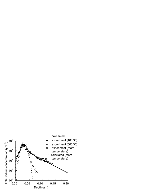
It is evident that in the first two cases, there is no phenomenon of channeling and it is possible to explain the formation of “tails” only by the anomalous impurity diffusion. It is worth noting that impurity diffusion can occur in an amorphous phase too, especially, if the high-current implanter is used for ion implantation and there is a possibility of substrate heating, as it was the case in the experiments of Cristiano et al. Cristiano-04 As an example, Fig. 1 presents the calculation of ion-implanted indium redistribution. The indium concentration profile was calculated within the framework of the model for diffusion of impurity interstitials described below. For comparison, the experimental data of Gamo-73 are used. In the work of Gamo et al. Gamo-73 the distributions of impurity atoms were obtained by measuring the -ray intensities in a combination with the layer removal technique. Indium was implanted with an energy of 45 keV to a dose of 11015 ion/cm2 and 8∘ off the axis in order to reduce channeling effects. The temperature of annealing was 900 ∘C, and the thermal treatment duration was 20 minutes. The following values of parameters for the model of interstitial diffusion of ion-implanted impurity were used. The parameters of the as-implanted indium distribution are: = 0.03 m (30 nm); = 0.0084 m (8.4 nm); the parameters of the indium interstitial diffusion are: the average migration length of indium interstitials = 0.042 m (42 nm); the time-average value of the generation rate of nonequilibrium impurity interstitials in the maximum of distribution = 7.9104 m-3s-1. Here and are the average projective range of impurity ions and straggling of the projective range, respectively. These parameters provide the best fitting of the calculated indium concentration profile to the experimental one.
As can be seen from Fig. 1, the results of calculation agree well with the experimental data. It is a very important argument in favour of the fast diffusion of nonequilibrium indium interstitials.

.
Taking into account the good agreement with the experimental data, we use the model of the interstitial diffusion of ion-implanted impurity for simulating indium redistribution during “hot” ion implantation that was investigated in Gamo-73 . The results of simulation are presented in Fig. 2. The energy and the dose of indium ions are the same as in the previous experiment, namely, 45 keV and 11015 ions/cm2. The following value of the average migration length of indium interstitials was used for the best fit to the experimental data: = 0.032 m (32 nm). This value is greater than the average migration length = 0.027 m used for similar calculations in Velichko-88 . Perhaps, the increase of is due to the effect of evaporation of indium interstitials from the surface of the semiconductor Kizilyalli-96 that we took into consideration in contrast to Velichko-88 . Taking into account the evaporation of indium interstitials made it possible to achieve the best agreement with the experimental profile in the vicinity of the surface.
.
As can be seen from Fig. 2, the results of calculation agree well with experimental data. The value of the average migration length for “hot” implantation of indium ions = 0.032 m is close to the migration length = 0.042 m for annealing of indium implanted layer at a temperature of 900 ∘C. It means that in the experiment with “hot” ion implantation a “tail” is also formed due to the fast migration of impurity interstitials.
The results obtained suggested to revise the inferences drawn in Blood-74 ; Dearnaley-75 about “tail” formation due to the scattering of ions into channels. Really, these inferences were based on the experiments Blood-74 with phosphorus ion implantation in thin silicon layers of different thicknesses. The main assumption of the above-mentioned paper is that diffusing phosphorus atom cannot pass through the boundary of the silicon crystal, while the ions which scatter into channels can cross the boundary due to the rest of the kinetic energy. However, within the framework of the interstitial diffusion model the “tail” formation is related to the diffusion of impurity interstitials. Therefore, there are no restrictions for impurity interstitials to evaporate from the surface of a crystal and then to collect on the substrate, on which the implanted layer is placed. This is confirmed by the experiments concerning hydrogen diffusion through thin silicon layers Wieringen-56 , because the extended “tails” on the hydrogen concentration profiles are also formed by interstitial diffusion Velichko-07 .
It is clear from the analysis carried out above that the vast majority of phenomena of “tail” formation in the low-concentration region of ion-implanted impurity profile is due to the fast impurity diffusion. The scattering of ions into channels can play only an auxiliary role in the experiments under investigation. It is usually supposed that impurity interstitials are the fast diffusing species Gamo-73 ; Crowder-71 ; Davies-68 ; Velichko-2010 . Let us note that the mechanism of the long-range migration of nonequilibrium impurity interstitials was already used for explanation of gold diffusion in ion-implanted layers Schulz-74 . This mechanism was also used for describing “tail” formation during thermal treatments of the layers implanted with boron Velichko-83 ; Velichko-2010 and for explanation of boron diffusion in “buried” layers under the conditions of generation of nonequilibrium silicon interstitials Cowern-90 ; Cowern-91 . Really, in Cowern-90 an analytical solution describing the redistribution of impurity atoms due to diffusion of boron interstitials during thermal treatment was obtained. As the initial condition for the distribution of boron atoms the -function was chosen. It was shown that for single participation of a boron atom in the act of interstitial migration a “tail” represents a straight line if the axis of concentration is logarithmic. It is necessary to note that for the initial boron distribution in the form of -function, the requirement of the occurrence of one event of boron interstitial migration is equivalent to the condition of the long-range migration of boron interstitials. On the other hand, under the condition of multiple migrations of the same impurity atom the boron profile has the form of Gaussian distribution Cowern-90 . Therefore, it was proposed in Cowern-91 to determine the microscopic mechanism of impurity transport by means of a change in the form of the impurity profile with increase in annealing duration. It is worth noting that the calculations which were carried out in Velichko-10 ; Velichko-11 ; Velichko-07 ; Velichko-2010 ; Velichko-2011 show that the “tail” representing a straight line is formed by the long-range migration of impurity interstitials not only in the case of initial distribution in the form of -function, but also for a generation rate of nonequilibrium interstitials described by the Gaussian distribution or any other distribution. Besides, the average migration length of impurity interstitials can be comparable with the characteristic size of the initial doped region, or even less than this size.
IV Model of interstitial diffusion
In the paper Velichko-08 , an equation for migration of nonequilibrium impurity interstitials was obtained which takes into account the different charge states of migrating species and also the drift of impurity interstitials in the built-in electric field and in the field of the elastic stresses. This equation has a form similar to the form of the equation describing the diffusion of nonequilibrium “impurity atom – intrinsic point defect” pairs when the influence of the built-in electric field and the field of the elastic stresses are also taken into account. As the mathematical formulations for the migration of nonequilibrium impurity interstitials and for the diffusion due to the nonequilibrium pairs are identical, it is impossible to make an exact conclusion about the kind of the mobile species from the form of impurity profile after thermal treatment. Let us consider for definiteness that boron transport during low-temperature annealing is carried out by migration of nonequilibrium impurity interstitials. We shall neglect the diffusion of the “impurity atom – intrinsic point defect” pairs in view of the small thermal budget. This assumption is based on the well-known opinion that impurity interstitials are the most mobile species. Taking into account that the extended “tail” is formed in the low-concentration region, where , we can suppose that the electric field does not influence the migration of impurity interstitials. Here is the concentration of the substitutionally dissolved boron atoms; is the intrinsic carrier concentration for the treatment temperature. It is clear that there is also no influence of the electric field in the case of migration of neutral interstitials even if . We shall also neglect the influence of elastic stresses and suppose that substitutionally dissolved boron atoms and boron atoms incorporated into clusters and extended defects are immobile. Then, the system of equations describing redistribution of ion-implanted boron during low-temperature annealing has the following form:
(i). The conservation law for immobile impurity atoms:
| (1) |
(ii). The equation of diffusion for nonequilibrium impurity interstitials:
| (2) |
or
| (3) |
where
| (4) |
Here is the total concentration of substitutionally dissolved impurity atoms and impurity atoms incorporated into clusters or trapped by extended defects (immobile impurity atoms): is the total concentration of nonequilibrium impurity interstitials in different charge states; and are the diffusivity and the average lifetime of nonequilibrium impurity interstitials, respectively; is the generation rate of impurity interstitials. We use the stationary diffusion equation for impurity interstitials in view of their large migration length (, where is the characteristic length of the decrease in the impurity concentration in the high-concentration region of impurity profile), and due to a small lifetime of these nonequilibrium interstitials (, where is the duration of annealing). Let us note that the system of equations (1), (2) is similar to the systems of equations used in Schulz-74 ; Velichko-83 ; Velichko-2010 ; Cowern-90 ; Cowern-91 for the description of interstitial diffusion.
To describe the spatial distribution of impurity atoms after implantation and spatial distribution of the generation rate of boron interstitials, the Gaussian distribution is chosen:
| (5) |
| (6) |
where
| (7) |
Here is the maximal concentration of impurity atoms after implantation; is the maximal value of generation rate of impurity interstitials per unit volume; is the dose of ion implantation [ion/cm2]; and are the average projective range of impurity ions and straggling of the projective range, respectively.
It is clear from expressions (5) and (6) that the model presupposes that the generation rate of boron interstitials is proportional to the total concentration of impurity atoms. Really, the analysis carried out in Velichko-2010 shows that the boron interstitials can be generated during thermal treatment not only as a result of annealing of radiation defects, but also due to dissolution or rearrangement of the clusters that incorporated impurity atoms and also as a result of elastic stresses arising due to the small atomic radius of boron. This assumption is confirmed by the experimental data of Gouye-10 , where the long-range migration of boron interstitials with the formation of the characteristic “tail” was observed during doping of the amorphous silicon layer deposited with the low thermal budget on a silicon substrate and then subjected to solid phase epitaxy. Thus, it follows from Gouye-10 that the long-range migration of boron interstitials is observed in the case of no radiation defects. As both the cluster concentration and intensity of elastic stresses are proportional to the total concentration of impurity atoms, the use of expression (6) for describing the generation rate distribution of boron interstitials is quite reasonable.
V Results of simulation of ion-implanted boron redistribution
In the case of the constant coefficients and the system of equations (1) and (3) allows obtaining an analytical solution. Such solutions for different boundary conditions on a finite interval within the assumption of continuous generation of impurity interstitials in the doped layer were obtained in Velichko-07 ; Velichko-2011 . We used these solutions for modeling the redistribution of ion-implanted boron. Let us note that the diffusivity has a constant value, if the migration of boron interstitials is not influenced by the built-in electric field. The average lifetime of these interstitials has a constant value in the case of absorption by the unsaturated traps distributed homogeneously in the bulk of a semiconductor. For example, such case of absorption is realized if replacement of the silicon atom by the boron interstitial from the lattice site to the interstitial one occurs.
Let us consider in the beginning the results of simulation of the experimental data of Yeong-08 , because in this investigation various methods of the transient enhanced diffusion suppression were used. So, in Yeong-08 for suppression of the transient enhanced diffusion Czochralski grown (100) -type silicon wafers were subjected to preamorphization by performing a germanium (Ge) ion implantation at 15 keV (Ge-PAI) and subsequently with 1 keV boron ions to a dose of 1.5 cm-2. Nitrogen (N) co-implantation to the same dose of 1.5 cm-2 was performed on some wafers. The thermal annealing was carried out in a rapid thermal processing system under N2 ambient duration at a temperature of 800 ∘C for 60 seconds. The dopant profiles were analyzed ex-situ by secondary ion mass spectrometry (SIMS). A primary Cross-sectional TEM (XTEM) was also performed to analyze the extent of amorphization and the Ge-PAI induced EOR defects. The simulation of boron redistribution carried out for these conditions in Velichko-11 , has shown good agreement with the experimental data for the average migration length of boron interstitials = 11 nm. Also it was supposed that approximately 8.6% of the implanted boron atoms occupied interstitial positions. Migration of these nonequilibrium interstitial atoms results in the formation of an extended “tail” on the boron concentration profile. This “tail” is located in the interval from 0.02 m up to approximately 0.1 m from the surface of a semiconductor. For comparison Fig. 3 presents the results of modeling for the same process of ion-implanted boron redistribution in the case of additional nitrogen implantation at 6 keV after preamorphization due to germanium ions Yeong-08 . The energy of nitrogen implantation equal to 6 keV was chosen so that the maximum of N concentration was located between the boron doped region and a/c interface.

.
As can be seen from Fig. 3, there is good agreement between the calculated profile and the experimental data. The following values of the model parameters were used to provide the best fit of the calculated boron concentration profile to the experimental one: Parameters prescribing the initial distribution of implanted boron: = 0.0044 m (4.4 nm); = 0.0036 m (3.6 nm). Parameters specifying the process of interstitial diffusion: the duration of annealing = 60 s; the annealing temperature T = 800 ∘C; the average lifetime of nonequilibrium boron interstitials = 0.011 s; the maximum value of the generation rate of nonequilibrium impurity interstitials = m-3s-1; the average migration length of boron interstitials = 5.9 nm; the concentration of boron interstitials on the right boundary = 0; the position of the right boundary = 0.5 m. It was supposed that approximately 21 % of the implanted boron atoms occupied the interstitial positions temporally.
As can be seen from the calculations performed, the additional implantation of nitrogen ions results in a significant (almost 2 times) reducing of the average migration length of boron interstitials. Therefore, the shrinkage of the “tail” approximately by 0.03 m is observed that is very attractive from the technological point of view. It is worth noting that there is a significant (2.8 times) increase in the generation rate of boron interstitials. However, due to the reduced migration length of these interstitials, their main fraction is trapped within the implanted layer that does not result in an increase of the depth of junction. We assume that this trapping is due to the interaction with nitrogen atoms or with complexes of nitrogen and germanium atoms.
A similar modeling for the case of transient enhanced diffusion suppression by using the lower annealing temperature, namely 750 ∘C, is presented in Fig. 4. The following values of the parameters specifying the process of interstitial diffusion were used: the maximum value of the generation rate of nonequilibrium impurity interstitials = m-3s-1; the average migration length of boron interstitials = 4.7 nm. It follows from the values obtained that the decrease of the annealing temperature results in the reduction of the average migration length of boron interstitials and in the highly abrupt impurity profile.

.
Now, let us present the results of modeling the interstitial diffusion during boron implantation using the data obtained in Cristiano-04 . In the paper Cristiano-04 , -type 10-20 cm, prime (100) Si wafers were used. The wafers were first preamorphized with Ge ions (30 keV, cm-2) to a depth of about 50 nm and then implanted with 0.5 keV boron ions to a dose of cm-2. The implants were performed on a high-current implanter at tilt and twist angles of 0∘ with electrostatic deceleration in front of the target. It is worth noting that due to the high-current implanter the wafer can be heated during ion implantation. The dopant atom distributions of all samples were analyzed using a high-resolution secondary ion mass spectrometry (SIMS). The boron concentration profile measured after implantation in preamorphized silicon is shown in Fig. 5.

.
As can be seen from Fig. 5, the calculated curve agrees well with the measured boron concentration profile after implantation characterized by the extended “tail”. Thus, the experimental data Cristiano-04 can be explained on the basis of the long-range migration of nonequilibrium boron atoms. Really, there is no channeling of ions due to implantation in the amorphous phase, whereas fast anomalous diffusion is quite possible in amorphous silicon. The following values of the model parameters were used to provide the best fit of the calculated boron concentration profile to the experimental one: Parameters prescribing the Gaussian distribution of implanted boron: = 0.0006 m (0.6 nm); = 0.0027 m (2.7 nm). Parameters specifying the process of fast diffusion: the maximum value of the generation rate of nonequilibrium impurity interstitials = 3.2m-3s-1; the average migration length of boron interstitials = 0.01 m (10 nm). For the best fit it was supposed that approximately 0.63 % of the implanted boron atoms participated in the long-range migration. However, there is also another way to explain the “tail” formation Cristiano-11 . Really, the boron ions were implanted with electrostatic deceleration in front of the target. During the deceleration stage, some ions can become neutral due to reciprocal collisions. In such a case they will not be decelerated and keep their original energy. Due to the higher energy, these ions penetrate deeper in the bulk of the semiconductor. Therefore, this problem requires a further investigation.
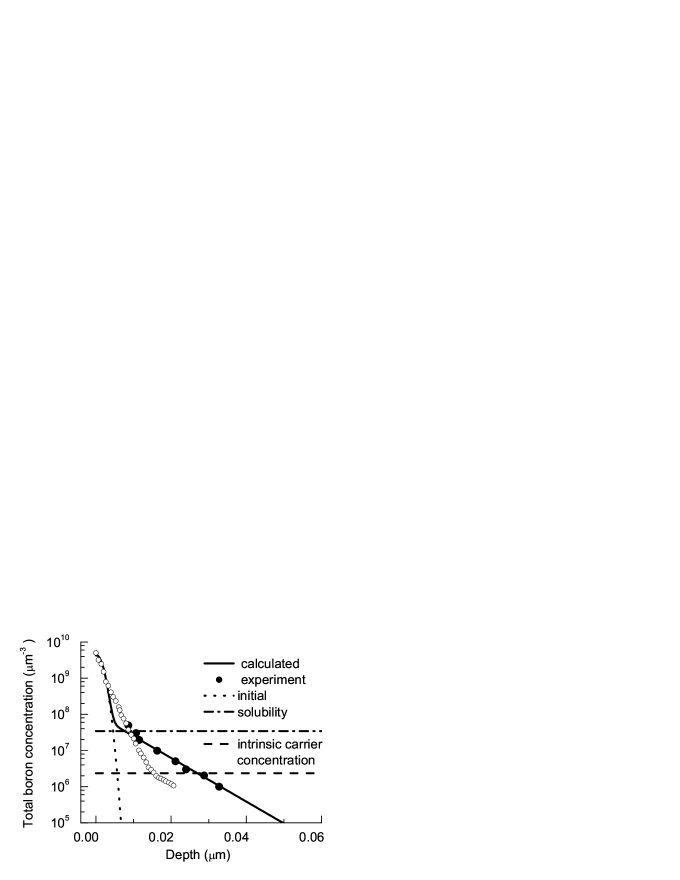
Finally, in Fig. 6 the results of modeling of ion-implanted boron redistribution are shown, when the implantation of BF2 ions was used for amorphization of the surface layer of silicon crystal and transient enhanced diffusion suppression Suzuki-01 . In Suzuki-01 , (100) oriented, 10 cm, -type silicon wafers were subjected to BF2 implantation at 2.2 keV to a dose of 1.0cm-2. The furnace annealing was carried out at a temperature of 800 ∘C for 30 minutes. The resulting boron concentration profiles were measured by SIMS. The following values of the model parameters were used to provide the best fit of the calculated boron concentration profile to the experimental one: Parameters prescribing the initial distribution of implanted boron: = 0.0002 m (0.2 nm); = 0.0014 m (1.4 nm). Parameters specifying the process of interstitial diffusion: the maximum value of the time-average generation rate of nonequilibrium impurity interstitials = 2.0m-3s-1; the average migration length of boron interstitials = 0.0072 m (7.2 nm). It was supposed that approximately 4.1 % of the implanted boron atoms occupied the interstitial positions temporally.
.
As is seen from Fig. 6, the calculated boron profile after furnace annealing agrees well with the experimental one in the “tail” region of impurity distribution that look like a straight line. It means that the “tail” region is formed due to the long-range migration of nonequilibrium boron interstitials. It is necessary to note that modeling of the experimental data obtained in Suzuki-01 was carried out earlier in the paper Marcon-08 . The model of Uematsu Uematsu-97 was used for simulation of boron diffusion in Marcon-08 . It is supposed in this model that there is a local thermodynamic equilibrium between substitutionally dissolved boron atoms, silicon self-interstitials, and boron interstitials. It means from the microscopic point of view that the same boron atom becomes frequently interstitial, makes a number of chaotic jumps, and then becomes substitutionally dissolved again due to the ”kick-out” of silicon atom from the lattice site. According to Cowern-91 , the impurity profile for this diffusion mechanism has a form of the Gaussian distribution. Really, the boron concentration profile calculated in Marcon-08 represents the Gaussian distribution and disagrees with the experimental data. On the other hand, as follows from the experimental data Suzuki-01 , the boron concentration profile after annealing for 1.5 h begins to get a convex form similar to the Gaussian distribution. Remaining within the framework of the model of the long-range migration, such a change in the form of impurity distribution can be explained by taking into account the significant increase in the boron concentration in the “tail” region. Really, if the impurity concentration is greater than the intrinsic carrier concentration , the migration of charged boron interstitials is influenced by the built-in electric field. On the other hand, the increase of annealing duration can create appropriate conditions for intensive dissolution of the clusters and extended defects incorporating silicon self-interstitials. In turn the generation of nonequilibrium self-interstitials results in boron diffusion due to the generation, migration, and dissolution of the “boron atom – silicon self-interstitial” pairs. It is usually supposed (see, for example, Velichko-84 ; Morehead-86 ; Mathiot-91 ; Bracht-07 ) that the local thermodynamic equilibrium prevails between substitutionally dissolved boron atoms, silicon self-interstitials, and the pairs. Therefore, the boron concentration profile formed due to the pair diffusion should look similar to the Gaussian distribution that agrees with the experimental data for large thermal budget. However, the final solution of this problem requires further careful investigations.
VI Conclusions
We have shown that the vast majority of the phenomena of “tail” formation in the low-concentration region of ion-implanted impurity profile, including ion implantation in the preamorphized silicon, “hot” ion implantation, impurity redistribution during the subsequent low-temperature annealing of ion-implanted layers, is related to the fast impurity diffusion. The channeling of ions scattered into channels is negligible for all the cases under consideration. With this purpose, simulation of indium redistribution during the subsequent annealing of ion-implanted layers and during “hot” indium implantation has been carried out. Many cases of the “tail” formation under different conditions of transient enhanced diffusion suppression during low-temperature annealing of boron implanted layers have been also investigated, including boron implantation into silicon preamorphized by germanium ions. The impurity concentration profiles calculated within the framework of the model of the long-range migration of nonequilibrium impurity interstitials agree well with experimental data. On this basis the values of the average migration length of nonequilibrium impurity interstitials have been obtained. So, if for boron implantation in silicon crystals preamorphized by germanium ions, the average migration length of boron interstitials is equal to 11 nm at an annealing temperature of 800 ∘C, the additional nitrogen implantation allows one to reduce this value approximately to 6 nm. A further reduction of the average migration length of boron interstitials can be achieved by decreasing the annealing temperature to 750 ∘C. Finally, for BF2 implantation in silicon crystals the average migration length of boron interstitials is equal to 7.2 nm at an annealing temperature of 800 ∘C.
References
- (1) D. De Salvador, E. Napolitani, G. Bisognin, M. Pesce, A. Carnera, E. Bruno, G. Impellizzeri, and S. Mirabella, Boron diffusion in extrinsically doped crystalline silicon. Phys. Rev. B. Vol.81, Art.No. 045209 (2010).
- (2) W.K. Hofker Implantation of boron in silicon. Philips Res. Repts. Suppl. No.8. pp.1-121 (1975).
- (3) A. E. Michel, W. Rausch, P. A. Ronsheim, R. E. Kastl, Rapid annealing and the anomalous diffusion of ion implanted boron into silicon. Appl. Phys. Lett. Vol.50, No.7. pp.416-418 (1987).
- (4) D. Fan, J. Huang, R. J. Jaccodine, P. Kahora, F. Stevie, Enhanced tail diffusion of ion implanted boron in silicon. Appl. Phys. Lett. Vol.50, No.24. pp.1745-1747 (1987).
- (5) A. E. Michel, W. Rausch, P. A. Ronsheim, Implantation damage and the anomalous diffusion of ion-implanted boron. Appl. Phys. Lett. Vol.51, No.7. pp.487-489. (1987).
- (6) D. J. Eaglesham, P. A. Stolk, H.-J. Gossmann, J. M. Poate, Implantation and transient B diffusion in Si: The source of the interstitials. Appl. Phys. Lett. Vol.65, No.18. pp.2305-2307 (1994).
- (7) P. A. Stolk, H.-J. Gossmann, D. J. Eaglesham, D. C. Jacobson, C. S. Rafferty, G. H. Gilmer, M. Jaraiz, J. M. Poate, H. S. Luftman, T. E. Haynes, Physical mechanisms of transient enhanced dopant diffusion in ion-implanted silicon. J. Appl. Phys. Vol.81, No.9. pp.6031-6050 (1997).
- (8) W. Lerch, M. Glück, N. A. Stolwijk, H. Walk, M. Schäfer, S. D. Marcus, D. F. Downey, J. W. Chow, Boron ultrashallow junction formation in silicon by low-energy implantation and rapid thermal annealing in inert and oxidizing ambient. J. Electrochem. Soc. Vol.146, No.7. pp.2670-2678 (1999).
- (9) K. Ohuchi, K. Adachi, A. Murakoshi, A. Hokazono, T. Kanemura, N. Aoki, M. Nishigohri, K. Suguro, Y. Toyoshima, Ultrashallow junction formation for sub-100 nm complementary metal-oxide-semiconductor field-effect transistor by controlling transient enhanced diffusion. Jpn. J. Appl. Phys. Vol.40, Pt.1, No.4B. pp.2701-2705 (2001).
- (10) S. Mirabella, A. Coati, S. Scalese, D. De Salvador, S. Pulvirenti, G. Bisognin, E. Napolitani, A. Terrasi, M. Berti, A. Carnera, A. V. Drigo, F. Priolo, Suppression of boron transient enhanced diffusion by c trapping. Solid State Phenom. Vols.82-84. pp.195-200 (2002).
- (11) S. C. Jain, W. Schoenmaker, R. Lindsay, P. A. Stolk, S. Decoutere, M. Willander, H. E. Maes, Transient enhanced diffusion of boron in Si. J. Appl. Phys. Vol.91, No.11. pp.8919-8940 (2002).
- (12) L. Shao, J. Liu, Q. Y. Chen, Wei-Kan Chu, Boron diffusion in silicon: the anomalies and control by point defect engineering. Mat. Sci. Eng. R. Vol.42. pp.65-114 (2003).
- (13) W. Lerch, S. Paul, J. Niess, S. McCoy, T. Selinger, J. Gelpey, F. Cristiano, F. Severac, M. Gavelle, S. Boninelli, P. Pichler, D. Bolze, Advanced activation of ultra-shallow junctions using flash-assisted RTP. Mat. Sci. Eng. B. Vols.124-125. pp.24-31 (2005).
- (14) H. Graoui, M. A. Foad, A comparative study on ultra-shallow junction formation using co-implantation with fluorine or carbon in pre-amorphized silicon. Mat. Sci. Eng. B. Vols.124-125. pp.188-191 (2005).
- (15) K. A. Gable, L. S. Robertson, A. Jain, K. S. Jones, The effect of preamorphization energy on ultrashallow junction formation following ultrahigh-temperature annealing of ion-implanted silicon. J. Appl. Phys. Vol.97, Art.No. 044501 (2005).
- (16) F. Lallement, D. Lenoble, Investigation on boron transient enhanced diffusion induced by the advanced P+/N ultra-shallow junction fabrication processes. Nuclear Instrum. Methods Phys. Res. Sect. B. Vol.237. pp.113-120 (2005).
- (17) E. M. Bazizi, P. F. Fazzini, A. Pakfar, C. Tavernier, B. Vandelle, H. Kheyrandish, S. Paul, W. Lerch, F. Cristiano, Modeling of the effect of the buried Si-SiO2 interface on transient enhanced boron diffusion in silicon on insulator. J. Appl. Phys. Vol.107, Art.No. 074503 (2010).
- (18) W. Y. Woon, C. L. Chen, Impact of ion implantation boundary dimensionality on boron transient diffusion in submicron scale patterns. Appl. Phys. Lett. Vol.97, Art.No. 121907 (2010).
- (19) T. Philippe, S. Duguay, D. Mathiot, D. Blavette, Atomic scale evidence of the suppression of boron clustering in implanted silicon by carbon coimplantation. J. Appl. Phys. Vol.109, Art.No. 023501 (2011).
- (20) Y. Shimizu, H. Takamizawa, K. Inoue, T. Toyama, Y. Nagai, N. Okada, M. Kato, H. Uchida, F. Yano, T. Tsunomura, A. Nishida, T. Mogami, Impact of carbon coimplantation on boron behavior in silicon: Carbon-boron coclustering and suppression of boron diffusion. Appl. Phys. Lett. Vol.98, Art.No. 232101 (2011).
- (21) S. Mirabella, D. De Salvador, E. Napolitani, F. Giannazzo, G. Impellizzeri, G. Bisognin, A. Terrasi, V. Raineri, M. Berti, A. Carnera, A.V. Drigo, F. Priolo, Self-interstitial diffusion and clustering with impurities in crystalline silicon. Nuclear Instrum. Methods Phys. Res. Sect. B. Vol.216. pp.80-89 (2004).
- (22) R. A. Camillo-Castillo, M. E. Law, K. S. Jones, Impact of dopant profiles on the end of range defects for low energy germanium preamorphized silicon. Mat. Sci. Eng. B Vols.114-115. pp.312-317 (2004).
- (23) F. Cristiano, N. Cherkashin, P. Calvo, Y. Lamrani, X. Hebras, A. Claverie, W. Lerch, S. Paul, Thermal stability of boron electrical activation in preamorphized ultra-shallow junctions. Mater. Sci. Eng. B. Vols.114-155. pp.174-179 (2004).
- (24) M. J. P. Hopstaken, Y. Tamminga, M. A. Verheijen, R. Duffy, V. C. Venezia, A. Heringa, Effects of crystalline regrowth on dopant profiles in preamorphized silicon. Appl. Surf. Sci. Vol.231-232. pp.688-692 (2004).
- (25) B. J. Pawlak, R. Surdeanu, B. Colombeau, A. J. Smith, N. E. B. Cowern, R. Lindsay, W. Vandervorst, B. Brijs, O. Richard, F. Cristiano, Evidence on the mechanism of boron deactivation in Ge-preamorphized ultrashallow junctions. Appl. Phys. Lett. Vol.84, No.12. pp.2055-2057 (2004).
- (26) B. J. Pawlak, W. Vandervorst, A. J. Smith, N. E. B. Cowern, B. Colombeau, X. Pages, Enhanced boron activation in silicon by high ramp-up rate solid phase epitaxial regrowth. Appl. Phys. Lett. Vol.86, Art.No. 101913 (2004).
- (27) B. J. Pawlak, R. Lindsay, R. Surdeanu, B. Dieu, L. Geenen, I. Hoflijk, O. Richard, R. Duffy, T. Clarysse, B. Brijs, W. Vandervorst, C. J. J. Dachs, Chemical and electrical dopants profile evolution during solid phase epitaxial regrowth. J. Vac. Sci. Technol. B. Vol.22, No.1. pp.297-301 (2004).
- (28) R. A. Camillo-Castillo, M. E. Law, K. S. Jones, L. M. Rubin, Influence of low temperature preanneals on dopant and defect behavior for low energy Ge preamorphized silicon, J. Vac. Sci. Technol. B. Vol.22, No.1. pp.312-316 (2004).
- (29) M. Tomita C. Hongo, M. Suzuki, M. Takenaka, A. Murakoshi, Ultra-shallow depth profiling with secondary ion mass spectrometry. J. Vac. Sci. Technol. B. Vol.22, No.1. pp. 317- 322 (2004).
- (30) R. Lindsay, K. Henson, W. Vandervorst, K. Maex, B. J. Pawlak, R. Duffy, R. Surdeanu, P. Stolk, J. A. Kittl, S. Giangrandi, X. Pages, K. van der Jeugd, Leakage optimization of ultra-shallow junctions formed by solid phase epitaxial regrowth, J. Vac. Sci. Technol. B. Vol.22, No.1. pp. 306-311 (2004).
- (31) J. J. Hamilton, K. J. Kirkby, N. E. B. Cowern, E. J. H. Collart, M. Bersani, D. Giubertoni, S. Gennaro, A. Parisini, Boron deactivation in preamorphized silicon on insulator: Efficiency of the buried oxide as an interstitial sink, Appl. Phys. Lett. Vol.91, Art.No. 092122 (2007).
- (32) M. Ferri, S. Solmi, D. Giubertoni, M. Bersani, J. J. Hamilton, M. Kah, K. Kirkby, E. J. H. Collart, N. E. B. Cowern, Uphill diffusion of ultralow-energy boron implants in preamorphized silicon and silicon-on-insulator. J. Appl. Phys. Vol.102, Art.No. 103707 (2007).
- (33) S. H. Yeong, B. Colombeau, K. R. C. Mok, F. Benistant, C. J. Liu, A. T. S. Wee, G. Dong, L. Chan, M. P. Srinivasan, The impact of nitrogen co-implantation on boron ultra-shallow junction formation and underlying physical understanding. Mat. Sci. Eng. B. Vols.154-155. pp.43-48 (2008).
- (34) O. I. Velichko, A. A. Hundorina, Modeling of the redistribution of boron atoms during annealing of silicon layers produced by high dose ion implantation. in: V. B. Odzhaev, V. V. Petrov, V. A. Pilipenko et al. (Eds.), Proceedings of IV International Conf. “Materials and Structures of Modern Electronics”, September, 23-24, 2010, Minsk, Belarus. pp.112-115 (2010) (In Russian).
- (35) O. I. Velichko, A. A. Hundorina, Change in the microscopic diffusion mechanisms of boron implanted into silicon with increase in the annealing temperature. arXiv:1105.4270v1[cond-mat.mtrl-sci].
- (36) R. A. Moline, Ion-implanted phosphorous in silicon: profiles using C-V analysis. J. Appl. Phys. Vol.42. pp.3553-3558 (1971).
- (37) P. Blood, G. Dearnaley, M. A. Wilkins, The origin of non-Gaussian profiles in phosphorus-implanted silicon. J. Appl. Phys. Vol.45, No.12. pp.5123-5128 (1974).
- (38) Crowder B. L. The influence of the amorphous phase on ion distributions and annealing behavior of group III and group IV ions implanted into Si. J. Electrochem. Soc. Vol.118, No.6. pp.943-952 (1971).
- (39) G. Dearnaley, G. A. Gard, W. Temple, M. A. Wilkins, Depth distribution of gallium ions implanted into silicon crystals. Appl. Phys. Lett. Vol.27, No.1. pp.17-18 (1975).
- (40) H. Ryssel, I. Ruge. Ion Implantation (John Wiley and Sons Inc; 99th edition, 1986) 478 pages.
- (41) K. Gamo, M. Iwaki, K. Masuda, S. Namba, S. Ishihara, I. Kimura, I. V. Mitchell, G. Ilic, J. L. Whitton, J. A. Davies, Enhanced diffusion and lattice location of indium and gallium implanted in silicon. Jpn. J. Appl. Phys. Vol.12, No.5. pp.735-741 (1973).
- (42) K. Gamo, K. Masuda, S. Namba, S. Ishihara, I. Kimura, Enhanced diffusion of high-temperature ion-implanted antimony into silicon. Appl. Phys. Lett. Vol.17, No.9. pp.391-393 (1970).
- (43) J. A. Davies, L. Eriksson, J. W. Mayer, Experimental evidence for interstitial In and Tl in ion-implanted silicon. Appl. Phys. Lett. Vol.12, No.8. pp.255-256 (1970).
- (44) S. Solmi, A. Parisini, M. Bersani, D. Giubertoni, V. Soncini, G. Carnevale, A. Benvenuti, A. Marmiroli, Investigation on indium diffusion in silicon. Appl. Phys. Vol.92, No.3. pp.1361-1366 (2002).
- (45) O. I. Velichko. Atomic Diffusion Processes under Nonequilibrium State of the Components in a Defect–Impurity System of Silicon Crystals. Ph.D. Dissertation. (Institute of Electronics of the National Academy of Sciences of Belarus, Minsk, 1988) (In Russian).
- (46) I. C. Kizilyalli, T. L. Rich, F. A. Stevie, C. S. Rafferty, Diffusion parameters of indium for silicon process modeling. J. Appl. Phys. Vol.80, No.9. pp.4944-4947 (1996).
- (47) A. Van Wieringen, N. Warmoltz, On the permeation of hydrogen and helium in single crystal silicon and germanium at elevated temperatures. Physica. Vol.22. pp.849-865 (1956).
- (48) O. I. Velichko, N. A. Sobolevskaya, Analytical solutions for the interstitial diffusion of impurity atoms. Nonlinear Phenom. Complex Syst. Vol.10, No.4. pp.376-384 (2007).
- (49) O. I. Velichko, N. V. Kniazhava, Modeling of the long-range interstitial migration of ion implanted boron. Comput. Mat. Sci. Vol.48. pp.409-412 (2010).
- (50) M. Schulz, A. Goetzberger, Controlled gold doping of silicon by using ion implantation. Appl. Phys. Vol.3. pp.275-280 (1974).
- (51) O. I. Velichko, Modelirovanie protsessa pereraspredeleniya ionno-implantirovannoi primesi pri korotkih nizkotemperaturnyh termoobrabotkah (Modeling of the process of ion implanted impurity redistribution under short low temperature thermal treatments) Abstracts of the 7 International Conf. on Ion Implantation in Semiconductors and Other Materials (Vilnius, September 27-29, 1983). pp.198-199 (In Russian).
- (52) N. E. B. Cowern, K. T. F. Janssen, G. F. A. van de Walle, D. J. Gravesteijn, Impurity diffusion via an intermediate species: The B-Si system. Phys. Rev. Lett. Vol.65, No.19. pp.2434-2437 (1990).
- (53) N. E. B. Cowern, G. F. A. van de Walle, D. J. Gravesteijn, C. J. Vriezema, Experiments on atomic-scale mechanisms of diffusion. Phys. Rev. Lett. Vol.67, No.2. pp.212-215 (1991).
- (54) O.I. Velichko, N.A. Sobolevskaya, Analytical solution of the equations describing interstitial migration of impurity atoms, Nonlinear Phenom. Complex Syst. Vol.14, No.1. pp.70-79 (2011).
- (55) O. I. Velichko, Macroscopic description of the diffusion of interstitial impurity atoms considering the influence of elastic stress on the drift of interstitial species. Phil. Mag. Vol.88, No.10. pp.1477-1491 (2008).
- (56) A. Gouyé, I. Berbezier, L. Favre, M. Aouassa, G. Amiard, A. Ronda, Y. Campidelli, A. Halimaoui, Insights into solid phase epitaxy of ultrahighly doped silicon. J. Appl. Phys. Vol.108, Art.No. 013513 (2010).
- (57) F. Cristiano, Private communication.
- (58) K. Suzuki, High-concentration diffusion profiles of low-energy ion-implanted B, As and BF2 in bulk silicon. Solid-State Electron. Vol.45, No.10. pp.1747-1751 (2001).
- (59) J. Marcon, A. Merabet, Diffusion modelling of low-energy ion-implanted BF2 in crystalline silicon: Study of fluorine vacancy effect on boron diffusion. Mat. Sci. Eng. B. Vols.154-155. pp.216-220 (2008).
- (60) M. Uematsu, Simulation of boron, phosphorus, and arsenic diffusion in silicon based on an integrated diffusion model, and the anomalous phosphorus diffusion mechanism. J. Appl. Phys. Vol.82, No.5. pp. 2228-2246 (1997).
- (61) O. I. Velichko, A set of equations of radiation-enhanced diffusion of ion-implanted impurities. in: I. I. Danilovich, A. G. Koval’, V. A. Labunov et al. (Eds.), Proceedings of VII International Conf. “Vzaimodeistvie Atomnyh Chastits s Tverdym Telom (Interaction of Atomic Particles with Solid)”, Part 2, Minsk, Belarus, 1984, pp.180-181 (in Russian).
- (62) F. F. Morehead, R. F. Lever, Enhanced “tail” diffusion of phosphorus and boron in silicon: Self-interstitial phenomena. Appl. Phys. Lett. Vol.48, No.2. pp.151-153 (1986).
- (63) D. Mathiot, S. Martin, Modeling of dopant diffusion in silicon: An effective diffusivity approach including point-defect couplings. J. Appl. Phys. Vol.70, No.6. pp.3071-3080 (1991).
- (64) H. Bracht, Self- and foreign-atom diffusion in semiconductor isotope heterostructures. I. Continuum theoretical calculations. Phys. Rev. B. Vol.75, Art.No. 035210 (2007).