Fluorescence and polarization spectroscopy of single silicon vacancy centers in heteroepitaxial nanodiamonds on iridium
Abstract
We introduce an advanced material system for the production and spectroscopy of single silicon vacancy (SiV) color centers in diamond. We use microwave plasma chemical vapor deposition to synthesize heteroepitaxial nanodiamonds of approx. 160 nm in lateral size with a thickness of approx. 75 nm. These oriented ’nanoislands’ combine the enhanced fluorescence extraction from subwavelength sized nanodiamonds with defined crystal orientation. The investigated SiV centers display narrow zero-phonon-lines down to 0.7 nm in the wavelength range 730-750 nm. We investigate in detail the phonon-coupling and vibronic sidebands of single SiV centers, revealing significant inhomogeneous effects. Polarization measurements reveal polarized luminescence and preferential absorption of linearly polarized light.
pacs:
I Introduction
In recent years, color centers in diamond have attracted research interest as candidates for solid state single photon sources. For this application they offer outstanding properties including high brightness and room temperature operation. The vast majority of experiments has been performed using single nitrogen vacancy (NV) centers, demonstrating key experiments towards quantum information applications including e.g. single photon emissionKurtsiefer et al. (2000); Beveratos et al. (2001) and coherent manipulation on optical transitions.Batalov et al. (2008) Nevertheless, as a single photon source NV centers suffer from a significant drawback, namely their broad room temperature emission bandwidth of about 100 nm caused by strong electron-phonon coupling.Kurtsiefer et al. (2000) Thus, alternative color centers with narrow (10 nm) room temperature emission namely nickel-nitrogen complexes (NE8),Gaebel et al. (2004) nickel-silicon complexes,Steinmetz et al. (2011); Aharonovich et al. (2009a) chromium related centersAharonovich et al. (2010, 2009b) and silicon vacancy (SiV) centersWang et al. (2006); Neu et al. (2011a, b) were investigated. Despite promising spectral properties, first studies on single SiV centers implanted into single crystal diamond showed unfavorably low single photon emission rates of only around 1000 counts per second (cps).Wang et al. (2006) However, more recent studies using single SiV centers contained in nanodiamonds revealed superior luminescence properties featuring emission rates up to 4.8 Mcps.Neu et al. (2011a, b) The emission is mainly concentrated in zero-phonon-lines (ZPLs) as narrow as 0.7 nm at approx. 738 nm, rendering SiV centers very promising candidates for narrowband, bright single photon sources. In Ref. Neu et al., 2011a, b randomly oriented nanodiamonds containing SiV centers produced in situ during chemical vapor deposition (CVD) growth were investigated. Spatially isolated nanodiamonds (70-140 nm in size) allowed for the optical addressing of bright single SiV centers. Additionally, the subwavelength size of the nanodiamonds yielded an efficient out coupling of the emitted fluorescence.Beveratos et al. (2001)
In this study, we combine the advantages of spatially isolated nanodiamonds with the defined orientation of a single crystal, enabling spectroscopy of single bright SiV centers in an environment of defined orientation. The advanced material system we use consists of (001) oriented nanodiamonds grown by heteroepitaxy on nanostructured iridium/yttria-stabilized zirconia/silicon substrates.Gsell et al. (2004); Fischer et al. (2008) Given the shape and the uniform orientation of the crystals we coin the term ’diamond nanoislands’. The samples will be discussed in detail in section II. The spectral properties of ensembles of SiV centers, i.e. vibronic sidebands as well as ZPL spectral width and position, have been investigated in the literature (e.g. Ref. Clark and Dickerson, 1991; Rossi et al., 1997; Sittas et al., 1996; Gorokhovsky et al., 1995; Feng and Schwartz, 1993). The variation of the local environment in which the different members of an ensemble reside is responsible for inhomogeneous line broadening. However, very little is known about these properties for single centers and their variation with the individual crystal environment (e.g. stress, proximity to other defects). With regard to the application of SiV centers as single photon sources, these inhomogeneous effects are significant as they determine the properties of individual single photon emitters, in particular the (in)distinguishability of single photons from different emitters. In the present work, we extensively study the inhomogeneous effects for single SiV centers analyzing the spectral properties of the ZPL as well as the vibronic sideband (section III). Beside the spectral properties knowledge of the orientation of the radiating dipoles of color centers is of crucial importance: First, it determines the fraction of the emission collected by the optics.Plakhotnik et al. (1995) Second, knowledge of the dipole orientation is critical for the coupling of color centers to photonic nanostructures such as nanowiresBabinec et al. (2010) or photonic crystals.Englund et al. (2010) Only one experimental work has so far addressed the emission dipole orientation of the SiV center.Brown and Rand (1995) We here present detailed investigations on absorption and emission dipoles of single SiV centers via polarization spectroscopy in section IV.
II Sample preparation and experimental setup
Diamond nanoislands are synthesized by microwave plasma chemical vapor deposition (MPCVD). Orientation of the grains is obtained by heteroepitaxial growth on a single crystal substrate. While different substrate materials have in principle shown the potential to serve as templates for oriented diamond growth, only iridium (Ir) fulfils the requirements for an essentially complete orientation of all the diamond grains and an unrivalled high nucleation density.Brescia et al. (2008) In addition, all experimental observations up to now indicate its inertness in the sense that Ir does not incorporate and generate any undesired luminescent centers in diamond.
The single crystal Ir films are grown on silicon (Si) via yttria-stabilized zirconia (YSZ) buffer layers. The YSZ films are prepared by pulsed laser deposition with a KrF excimer laser (pulse duration 25 ns; pulse energy 850 mJ) on Si(001) substrates using a cylindrical ablation target with a stoichiometry of 21.4 mol% YO1.5. Ablation is performed at a temperature of 750∘C. In order to reduce the native oxide, the first 300 pulses are performed in high vacuum. During the subsequent growth the oxygen background pressure is increased to 510-2 Pa. For more details see Ref. Gsell et al., 2009. In contrast to our standard procedure Gsell et al. (2009) which aims at flat films, we modify the Ir deposition in order to generate a nanostructured film-surface with flat (001) top facets bounded by steep side faces. This rougher topography facilitates the formation of isolated nucleation areas in the subsequent bias enhanced nucleation (BEN) procedure.
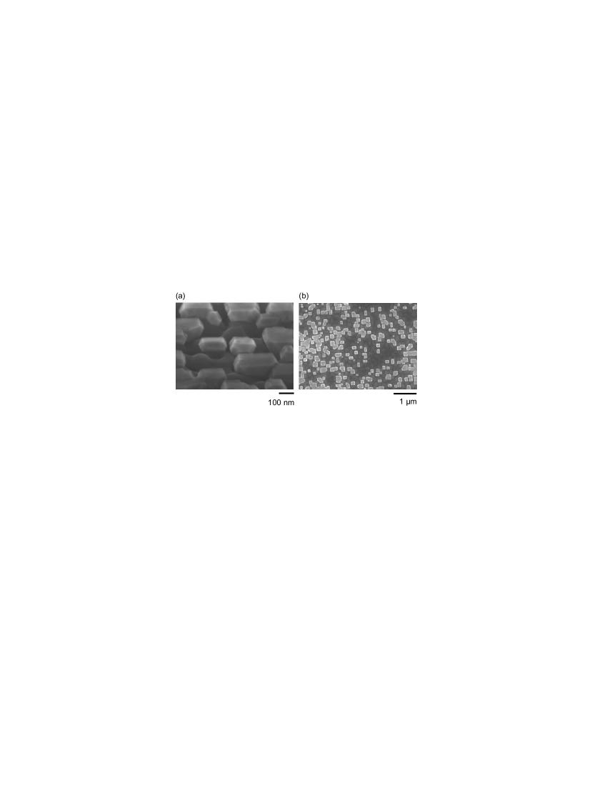
Diamond deposition was performed in an IPLAS reactor equipped with a CYRANNUS plasma source. During the BEN step the methane concentration in the CH4/H2 gas mixture is 3%.Gsell et al. (2004) The pressure in the plasma reactor is 40 mbar, the microwave power 2000 W and the substrate temperature 800∘C. A negative bias voltage of -300 V is applied to the substrate in order to induce an intensive ion bombardment which is necessary to generate epitaxial diamond nuclei. After switching off the bias voltage, the microwave plasma growth conditions with 0.5% CH4 in H2 are maintained for 20 min. During the growth stage the diamond nuclei transform into epitaxial diamond crystals with a mean lateral size of 160 nm (standard deviation of 60 nm). From SEM images (see Fig. 1) of the tilted sample, the cubo-octahedral shape of the nanodiamonds with {001} and {111} faces can be clearly identified.Wild et al. (1993) We estimate a thickness of 75 nm (standard deviation of 12 nm). Thus, the nanoislands fulfill the requirements of subwavelength size to enable efficient fluorescence extraction with negligible total internal reflection. A low density of SiV centers is created in situ due to plasma etching of the silicon substrates and incorporation of silicon into the growing diamond.Neu et al. (2011a)
Single SiV centers are detected via confocal laser fluorescence microscopy. To excite the color centers we employ a cw tunable Titanium-Sapphire laser (Matisse, Sirah) operated at 694-696 nm. This close to resonance excitation wavelength matches absorption bands of the SiV center.Iakoubovskii et al. (2001) The laser is focussed by a high numerical aperture microscope objective (Olympus, magnification 100x, NA 0.8). The fluorescence is collected by the same objective and separated from reflected laser light by a dichroic mirror and bandpass filters. For correlation measurements, we employ a Hanbury-Brown-Twiss setup with two avalanche photodiodes (Perkin Elmer SPCM AQRH-14) featuring a typical quantum efficiency of 70%. Correlation measurements are performed by recording the arrival times of the photons (Pico Quant, Pico Harp, timing resolution of electronics 4 ps, photo diode timing jitter 354 ps) and calculating the correlation functions. To analyze the spectral properties of the color center fluorescence we employ a grating spectrometer (Horiba Jobin Yvon, iHr550). A grating with 600 grooves/mm here enables a resolution of approx. 0.18 nm. All experiments were performed at room temperature.
III Fluorescence spectroscopy on single SiV centers in nanoislands
III.1 Properties of the Zero-Phonon-Line

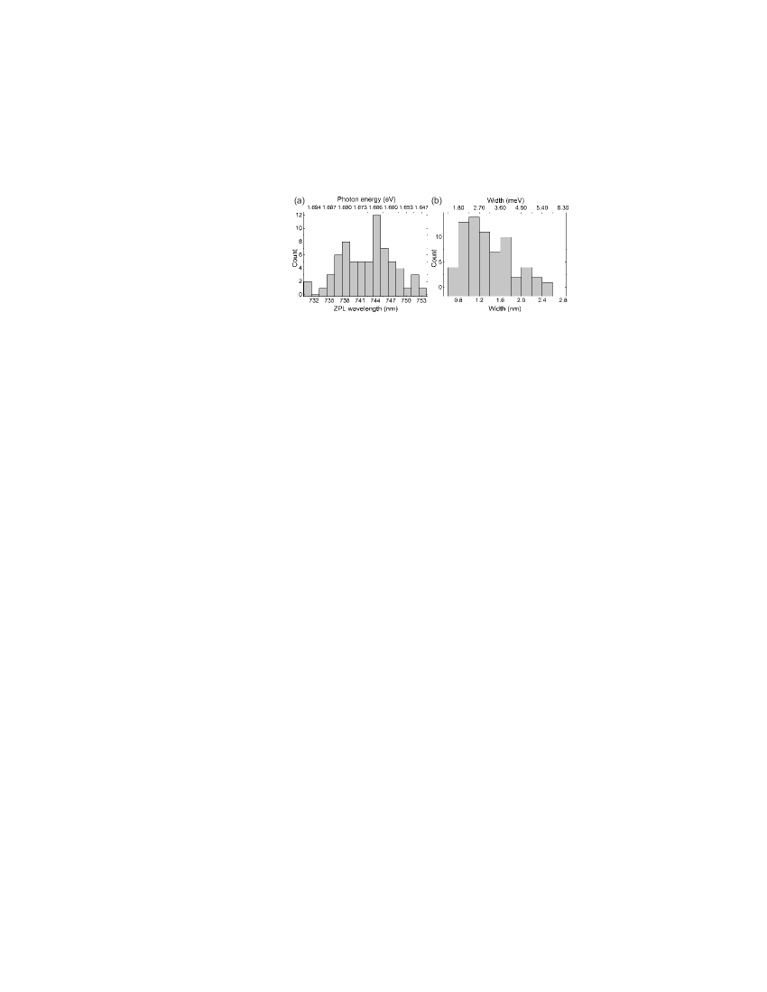
Fig. 2(a) displays 5 typical spectra of single SiV centers. Measurements of the intensity autocorrelation function (g(2)) of the emitted fluorescence identify all color centers as bright single emitters with single photon count rates of 0.2-6 Mcps. All measured g(2) functions indicate three level population dynamics of the SiV centers as observed earlier.Neu et al. (2011a) For the different investigated emitters we do not find a clear correlation between the g(2) function parameters and the emitters’ spectral properties (ZPL position and width). The spectra of all investigated emitters reveal intense zero-phonon-lines (ZPLs) around 740 nm. A histogram of the spectral positions of the ZPLs is given in Fig. 3(a). The observed positions spread over about 20 nm. The mean value of the position is 742.6 nm (standard deviation 5.1 nm). The measured linewidth varies between 0.7 and 2.5 nm with a mean value of 1.3 nm (standard deviation 0.4 nm). We point out that no correlation between spectral position and linewidth has been found. Thus, mechanisms broadening the ZPLs and shifting them seem to be independent. We further point out that no correlation between brightness of the emitters and line position or spectral linewidth is observed.
Evidence for environment dependent lineshifts and thus inhomogeneous broadening in ensembles is found in the literature: room temperature ZPL widths up to 15 nm (35 meV) have been reported in polycrystalline diamond (PCD),Zaitsev (2001) accompanied by asymmetric lineshapes and splitting of the ZPL into multiple lines in the range of 733-745 nm. The broadening is explained by mechanical stress between crystallites.Zaitsev (2001) Similarly, for SiV centers in PCD with less broadened ZPLs (17 meV, 7.4 nm, 77 K) a trend towards an asymmetric tail of the ZPL at longer wavelength is observed, hinting at a preferential red shift.Clark et al. (1995) The low temperature (10 K) linewidth observed for SiV ensembles in PCD still amounts to about 4.4 nm (10 meV), indicating a significant temperature independent inhomogeneous broadening.Feng and Schwartz (1993) The spread of the line positions of single SiV centers in our experiments is thus comparable to the inhomogeneous broadening of ensembles in PCD. The ZPL position can be shifted by stress (see Ref. Sternschulte et al., 1995, 1994, stress in -direction) or by external magnetic (Zeeman-effect) or electric fields (Stark-effect). No data on the Stark-effect for SiV centers is available in the literature and the Zeeman-effect is very weak.Sternschulte et al. (1995) Thus, residual mechanical stress in the nanodiamonds is most likely the major source for the observed ZPL lineshifts.
For diamond islands on a foreign substrate several different mechanisms for stress formation have to be considered: First, stress builds up owing to the mismatch in the coefficients of thermal expansion (CTFs) between the substrate and diamond. In the present case the massive Si substrate induces a biaxial compressive stress of -0.68 GPa in the tiny diamond crystals when the sample is cooled down from deposition temperature to room temperature at the end of the growth process.Gsell et al. (2004) The geometric shape of isolated crystals corresponds to a truncated pyramid. In contrast to a closed diamond film, a certain fraction of the imposed stress can relax elastically. The amount of stress relaxation varies with the local position within the crystallites.Schreck et al. (2000) Coherency stress is a second contribution specifically important in heteroepitaxial material systems. The lattice constant of Ir is 7.6% higher than that of diamond. Pseudomorphic growth would yield an unrealistically high in-plane stress of +89 GPa. As a consequence misfit dislocations are introduced from the very first stage of film growth and relaxation of misfit stress occurs. In a former detailed stress analysis of a 0.6 m diamond layer on Ir/SrTiO3(001) a residual coherency stress of +0.9 GPa was deduced.Schreck et al. (2000) Various measurements for 0.5-1 m thick diamond films on Ir/YSZ/Si(001) indicate even lower values compatible with an essentially complete stress relaxation of the diamond films.Gsell et al. (2011) Growth stress is a third source that results from the interaction of initially isolated grains when they merge during lateral growth. In PCD films nearly exclusively tensile stress is found which is attributed to attractive grain boundary forces typically explained in the framework of the grain boundary relaxation model.Windischmann and Epps (1992) In Ref. Schreck et al., 2000 a growth stress of +0.3 GPa was reported.
The previous considerations mainly refer to macro stress. However, as described in Ref. Jiang and Jia, 1996, during the coalescence of slightly misoriented grains, small angle grain boundaries can be substituted by disclinations and finally the initially individual crystals can continue growth as one single crystal. The coalescence process is accompanied by a strong local bending of the crystal lattice yielding high amplitudes of micro stress. Former studiesBrescia et al. (2008) revealed a density of 2 cm-2 epitaxial diamond grains on Ir after BEN and 10 s growth. According to these observations we estimate that about 10 grains have merged to form the present nanoislands. Due to the extremely high activation energy for the gliding of dislocations in diamond we assume that most of the dislocations are still present in the islands of our sample. The associated micro stress fields are locally experienced by the optical centers and induce the observed distribution of ZPL positions.
For SiV centers to our knowledge there exists only one measurement of stress shift rates in the literature: in Ref. Sternschulte et al., 1995, 1994 stress shifting and quenching of the SiV fine structure have been investigated at low temperatures and for compressive stress applied in -direction. Shift coefficients in the range of -9 to 8.6 meV GPa-1 have been determined for different fine structure components. However, there are neither measurements of lineshift coefficients at room temperature nor investigations of lineshifts for stress applied in other directions. Thus, we can state that the observed large spread in ZPL positions is due to the locally varying micro stress fields but absent knowledge of both lineshift coefficients and stress orientation preclude determination of the stress field magnitude. We point out that the observed significant susceptibility of SiV centers to environmental changes also potentially offers controlled wide range tunability of ZPL wavelengths, already demonstrated for chromium related centers via electric fields.Mueller et al. (2011) In the presence of inhomogeneous effects, resonance tuning is crucial for quantum information applications considering production of indistinguishable photons.
III.2 Vibronic coupling and vibronic sideband features
Even at room temperature, vibronic sideband emission of the SiV center is weak compared to the ZPL, as seen in Fig. 2(b), thus disclosing weak electron-phonon coupling. This observation is consistent with a trend reported in the literature, i.e. generally color centers involving heavier impurities tend to exhibit low electron-phonon coupling.Zaitsev (2000) The strength of the electron-phonon coupling is measured by the Huang-Rhys-Factor . The intensity M of the phonon sideband is given by: Davies (1981)
| (1) |
For SiV center ensembles is reported in absorption (Ref. Collins et al., 1994), while for single SiV centers in nanodiamonds fluorescence spectra reveal .Neu et al. (2011a)

Fig. 4 shows a histogram of the room temperature Huang-Rhys-Factors estimated from the fluorescence spectra of single SiV centers after correcting for broadband background fluorescence originating from the nanoislands. The observed Huang-Rhys-Factors are slightly higher than reported for ensembles, the mean value amounts to 0.38 with a standard deviation of 0.12. For the majority of the SiV centers more than 70% of the fluorescence is concentrated in the ZPL, thus rendering the SiV center especially suitable as a low bandwidth emitter. We point out that we observe 5 emitters with noticeably higher Huang-Rhys-Factor (). As discussed in the following, the Huang-Rhys-Factors might be overestimated due to misinterpretation of electronic transitions as vibronic sidebands. We emphasize that we find no correlation between the ZPL position and the Huang-Rhys-Factor.
As clearly visible from Fig. 2(b) the sideband structure of individual SiV centers varies significantly. In the following we analyze the origin of the sideband features as well as the variations. For the measured average Huang-Rhys-Factor of the relative intensities compared to the ZPL are 38% for the one phonon sideband and only 7% for the two-phonon sideband. Thus, we do not expect to observe sidebands related to two-phonon processes for SiV centers at room temperature and analyze the observed sidebands in terms of one phonon processes in the following. Electronic transitions of color centers couple to two types of vibrational modes: lattice modes corresponding to vibrations of the undisturbed diamond lattice and local or quasi-local modes. The latter are specific of the defect, representing vibrations involving the defect and its neighboring carbon atoms.Lin-Chung (1994)
Coupling to lattice modes is governed by the phonon-density of states of the diamond lattice, which has been calculated and measured in the literature (e.g. Ref. Lin-Chung, 1994; Wehner et al., 1967; Zaitsev, 2000; Windl et al., 1993). Electronic transitions predominantly couple to phonons with wave-vectors at high symmetry points of the Brillouin zone (critical points).Feng and Schwartz (1993) A list of the phonon energies corresponding to these critical points has been determined in Ref. Solin and Ramdas, 1970 and is displayed in table 1. The phonon density of states has a sharp high energy cut off at 165 meV and diminishes strongly below approx. 70 meV.Lin-Chung (1994); Zaitsev (2000); Wehner et al. (1967); Windl et al. (1993) Therefore, all sideband features below 70 meV or above 165 meV are attributed to local modes. Local modes within the energy range of lattice phonons are referred to as quasi local. The vibronic sidebands of the SiV center were experimentally examined in several publications as summarized in table 1.
Simulations using estimated force constants for the diamond lattice and the SiV defect in Ref. Lin-Chung, 1994 indicate the existence of high energy local modes (see also table 1).
| Method | Sideband energies (meV) | ||||||||
|---|---|---|---|---|---|---|---|---|---|
| PL 515 nmClark and Dickerson (1991) | 63 | 123 | 154 | ||||||
| PL 457 nmRossi et al. (1997) | 60 | 120 | |||||||
| AbsorptionCollins et al. (1994) | 33 | ||||||||
| PL 488/514 nmSittas et al. (1996) | 36 | 64 | 83111interpreted as electronic transitions by Sittas et al.Sittas et al. (1996) | 125111interpreted as electronic transitions by Sittas et al.Sittas et al. (1996) | 155111interpreted as electronic transitions by Sittas et al.Sittas et al. (1996) | ||||
| PL 488 nmSternschulte et al. (1994) | 42 | 65 | 85 | 126 | 153 | 166 | |||
| PL 737 nmGorokhovsky et al. (1995) | 42 | 64 | 125 | 148 | 155 | 163 | |||
| PL 515 nmFeng and Schwartz (1993) | 43 | 67 | 104 | 129 | 155 | ||||
| SimulationLin-Chung (1994) | 56 | 80 | 107 | 165222several modes are predicted between these values, they are skipped for clarity. | 184222several modes are predicted between these values, they are skipped for clarity. | ||||
| 81 | 168222several modes are predicted between these values, they are skipped for clarity. | 187222several modes are predicted between these values, they are skipped for clarity. | |||||||
| critical pointsSolin and Ramdas (1970) | 70 | 100 | 122222several modes are predicted between these values, they are skipped for clarity. | 138222several modes are predicted between these values, they are skipped for clarity. | 150222several modes are predicted between these values, they are skipped for clarity. | ||||
| 113 | 133222several modes are predicted between these values, they are skipped for clarity. | 147222several modes are predicted between these values, they are skipped for clarity. | 155222several modes are predicted between these values, they are skipped for clarity. | ||||||

Fig. 5 displays a histogram of the sideband energies observed for single SiV centers. The positions are derived from the fluorescence spectra by applying a multi peak Lorentzian fit to the baseline corrected spectra (see Fig. 2(b)). The observed sidebands span the whole range observed in ensembles (cf. Tab. 1), no clear concentration on distinct sideband energies is observed, except around 170-180 meV. In accordance with the literature we observe low energy local modes around 30-40 meV, as well as high energy local modes beyond 165 meV. We point out that we observe high energy sidebands above 180 meV predicted by simulations (Ref. Lin-Chung, 1994) but not yet experimentally detected. In the energy region of lattice phonons only a weak concentration around the critical points is observed. The relative intensity of the various sidebands changes significantly, evidencing preferential coupling to different modes (see Fig. 2(b)). We interpret the observed spread of sidebands in terms of changing electron-phonon coupling for different emitters, also indicated by the varying Huang-Rhys-Factors.
In the literature several reports indicate that sidebands and thus electron-phonon coupling strongly depend on the local environment. Sternschulte et al. Sternschulte et al. (1994) report that a sideband feature shifted by 166 meV was only observed on some positions on a CVD grown homoepitaxial sample. Iakoubovskii et al. Iakoubovskii et al. (2001) find a correlation between the width of the Raman-peak of the CVD film, i.e. the stress present in the film and the sidebands of the SiV center: in highly stressed films broadband emission dominates over distinct sideband features. Gorokhovsky et al. Gorokhovsky et al. (1995) also report that in PCD no well resolved sideband features were observed under non-resonant 514 nm laser excitation, indicating averaging over centers with differing sideband spectra. In contrast, for resonant excitation of the same sample with 737 nm a defined sideband structure evolves. The authors in Ref. Gorokhovsky et al., 1995 attribute this to the excitation of a sub-ensemble with ZPL at the excitation laser wavelength. This sub-ensemble within the inhomogeneously broadened line exhibits defined and identical sideband features, while the sideband structure is averaged out upon excitation of all inhomogeneously broadened SiV centers. If the resonant excitation is tuned to longer wavelengths, the most prominent sideband feature at 64 meV shifts to lower phonon energies (2.5 meV, excitation tuned from 736-739 nm). The shifting behavior for a higher energy sideband at 125 meV, however, shows no clear trend. Thus, distinct sidebands may respond differently to environmental changes that shift the ZPL accompanied also by changes in the linewidth of the phonon replicas.Gorokhovsky et al. (1995) We here observe the varying sideband spectra directly via observation of single emitters. Thus, we exclude inhomogeneous effects in sub ensembles. The observed variety of single emitter sideband spectra is in accordance with previous ensemble observations.
As visible from Fig. 2(b) some SiV centers show remarkably narrow emission lines in the sideband region. Specifically, around 825-845 nm individual SiV centers even show multiple narrow lines. Fig. 6 displays the observed features plotted versus their width, indicating an accumulation of narrow features in the spectral region from 825-845 nm. The narrow linewidth suggests that these features are due to electronic transitions rather than vibronic sidebands. However, the identification of sidebands and electronic transitions is not always clear as for defects involving heavy impurities sideband features due to local modes might be as narrow as the ZPL itself.Zaitsev (2000) Nevertheless, in low temperature experiments Sittas et al. Sittas et al. (1996) observe a significant spectral narrowing of the three highest energy sidebands of the SiV {776 nm (83 meV), 797 nm (125 meV) and 812 nm (155 meV)} and thus attribute them to purely electronic rather than vibronic transitions. As in previous studies of SiV centers photon correlation measurements provided evidence for three level population dynamics,Wang et al. (2006); Neu et al. (2011a, b) one might expect a second purely electronic transition. In addition, very recent studies report absorption of SiV ensembles between 830-850 nm.D’Haenens-Johansson et al. (2011) Therefore, we tentatively attribute the observed features to electronic transitions from a second excited state to the ground state. We point out that spectral features above 900 nm are strongly suppressed in our setup for technical reasons (dichroic transmission, spectrometer efficiency): The detection efficiency is only approx. 0.25% of the efficiency at 750 nm. Thus, we would not expect to observe e.g. the 946 nm line recently reported as a further electronic transition of the SiV center.D’Haenens-Johansson et al. (2011)

IV Polarization spectroscopy

In this section, we investigate the polarization dependent absorption of the SiV centers, as well as the polarization properties of the emitted fluorescence light. For the first measurement a half-wave plate is used to rotate the excitation laser polarization while recording the emitted fluorescence intensity. To ensure that the fluorescence is proportional to the absorbed intensity, excitation powers far below saturation are employed. To determine the polarization of the emitted light a linear polarization analyzer is rotated in the detection path. Different absorption processes are possible for color center excitation. For defect to band excitation electrons excited to the conduction band relax via defect states. As the ground state of the SiV center was reported about 2.05 eV (Ref. Iakoubovskii and Adriaenssens, 2000) below the conduction band edge, we exclude this path for our 1.78 eV (695 nm) excitation. The absorbing transition can also be provided via transitions to higher vibronic states in the excited state or higher excited electronic states of the color center, thus identification of the absorbing transition is unclear. If the SiV center behaves like a single dipole in absorption one expects a sinusoidal characteristics with minima close to zero for excitation with linearly polarized light, as no light is absorbed if its polarization is perpendicular to the dipole axis. The visibility
| (2) |
of a single dipole in absorption amounts to 100%. Additionally, the absorption only addresses the dipole component in the sample plane (i.e. plane perpendicular to the excitation laser propagation direction, here (001) plane of the diamond).Ha et al. (1999) Dipoles oriented in that plane show maximum absorption, while dipoles oriented perpendicularly are effectively not excited. All SiV centers investigated show very high visibility in absorption between 90% and 100%. Thus, we conclude that SiV centers exhibit a single dipole in absorption ( type transition). The deviations from 100% visibility are attributed to experimental imperfections. First, to determine the contrast in the polarization dependent excitation curves we correct for background luminescence of the diamond material. As the background exhibits spatial variations in the vicinity of the defects, this procedure introduces an uncertainty of 5-10%. Second, the dichroic mirror used to separate excitation laser light and color center luminescence induces polarization changes, leading to an orientation dependent loss of linear polarization: for s and p polarization reflected laser light maintains 100% polarization visibility, for 45 degrees we measure a reduction to about 90%.

Similar to the absorption, we observe high polarization visibility in the range of 86% to 100% for the fluorescence, thus evidencing linearly polarized emission. The absence of depolarization hints at vanishing influences of reorientation processes in the excited state that would lead to depolarization of the emitted light.Clark et al. (1962) Furthermore, from the measured polarization dependence we infer that emission and absorption dipoles of the SiV centers are parallel within experimental error. Fig. 8 gives a histogram of the observed deviations, the maximum deviation is 8.2 degrees, the mean value is 2.3 degrees. For a purely statistical measurement error we would expect the mean value of the deviations to be zero. We thus interpret this result as an offset of 2 degrees of the polarization scale for absorption and emission. We point out that a parallel orientation of absorption and emission dipoles is very common e.g. for organic molecules (Ref. Ha et al., 1999) and has also been considered for other vacancy based color centers for -type absorption and emission dipoles.Bergman et al. (2007) Recent studies on chromium related centers also found parallel orientations for emission and absorption dipoles, however, with significantly varying orientations in the diamond lattice.Mueller et al. (2011)

In the following we aim at interpreting our polarization measurements in terms of orientation of the color center dipole with respect to crystal axes and electronic states involved in the transition. For this interpretation we have to consider that the absorption measurements only reveal the dipole component in the sample plane. On the other hand, care has to be taken in interpreting emission polarization: First, the presence of the metal surface might distort the polarization of the emitted light. Second, due to imaging through a high NA objective, loss of polarization contrast occurs for linearly polarized emission.Fourkas (2001) For a dipole in the sample plane we would expect 100% visibility, whereas for a dipole perpendicular to that plane polarization contrast fully vanishes, a 45 degrees tilt yields 70% visibility (NA 0.8). Thus, in principle, assuming a single dipole, one may use the visibility as well as the position of maxima and minima to determine the three-dimensional orientation of the dipole.Fourkas (2001) Nevertheless, the considerations in Ref. Fourkas, 2001 only hold for a dipole in an isotropic medium. SiV centers in nanodiamonds on an Ir surface constitute a highly anisotropic situation, leading to a strongly modified radiation pattern close to the metal surface.Neu et al. (2011a) Taking also into account the issue of background substraction, we therefore consider the polarization contrast non reliable to determine the tilt of the dipole with respect to the sample plane in our case. Fig. 9 displays a histogram of the orientations of the SiV dipole in the sample plane deduced from absorption measurements. We note that the nanoislands crystal directions in the (001) plane align with the sample edges and we identify a 0 degrees orientation of the azimuthal angle with the [110] direction.
Generally, point defects in diamond may have their highest symmetry axis oriented along , or axes.Kaplyanskii (1963) For oriented defects 3 equivalent sites have to be considered, while there are 6 equivalent sites for and 4 equivalent sites for oriented defects.Brown and Rand (1995) Due to symmetry considerations transition dipoles are either parallel to the high symmetry axis (z-dipole) or perpendicular (x,y-dipoles).Brown and Rand (1995) Based on measurements of polarized luminescence Brown et al. Brown and Rand (1995) identify a z-dipole for the ZPL transition of the SiV center. Following their line of argument, we assume a z-dipole for the interpretation of the orientation data. For our (001) oriented sample, one expects dipole orientations in the sample plane of -45 and 45 degrees for oriented transition dipoles, while for oriented defects orientations -90 degrees, 0 and 90 degrees occur. oriented defects on the other hand, lead to measured dipole orientations of -90, -45, 0, 45 and 90 degrees. Whereas we observe a certain scatter in orientations, the measured data, nevertheless, best match a defect orientation and exclude and orientations (see Fig. 9). SEM images imply that the spread of dipole orientations is not due to misorientation (twist and tilt) of the diamond nanoislands. In summary, our findings are similar to those of Brown et al. Brown and Rand (1995), identifying the SiV center as a oriented defect with a z-dipole. Brown et al. assign the defect to be of monoclinic I or rhombic I symmetry.Brown and Rand (1995) We now compare our observations to theoretical models discussed in the literature. Goss et al.Goss et al. (1996, 2007) model the SiV center as a negatively charged defect with D3d symmetry, the silicon atom being located in a so called split-vacancy configuration. Their calculations identify a transition as the 1.68 eV ZPL. At low temperature the ZPL splits into 4 components.Clark et al. (1995); Sternschulte et al. (1994) The splitting is attributed to a Jahn-Teller-effect in this model. The light emitted by a transition (D3d), however, is unpolarized according to Kaplyanskii.Kaplyanskii (1963) Thus, this model does not fit our experimental observation. An alternative model introduced by Moliver in Ref. Moliver, 2003 on the other hand assumes the center being in the neutral charge state (SiV0). The silicon atom is shifted off center along the direction yielding symmetry. The splitting is explained in terms of a tunneling of the Si atom between equivalent sites. The 1.68 eV ZPL is associated with a transition. Here the transition between states would be linearly polarized.Kaplyanskii (1963) Thus, our polarization data would support this model of the SiV0. Nevertheless, the orientation data does not fit the symmetry proposed therein. Furthermore, the interpretation as SiV0 defect is questionable, as the SiV0 defect has recently been identified as the source of 1.31 eV emission using optical and electron paramagnetic resonance techniques.D’Haenens-Johansson et al. (2011) In summary, the measured dipole orientations imply a lower symmetry of the defect than predicted by prevalent theoretical models and assignment of transition polarizations and charge states seem questionable. To provide a reliable matching of theoretical prediction and experimental data a more precise determination of the dipole orientation as well as further theoretical work are necessary.
V Conclusion
We extensively investigated the spectral properties of single SiV centers produced in situ during CVD growth. As advanced material system we employ 160 nm large, 75 nm thick heteroepitaxially grown nanoislands on Ir/YSZ/Si substrates, thus combining enhanced fluorescence extraction and defined crystal orientation. We find intense, narrow (0.7-2.5 nm) ZPLs at around 740 nm. Residual stress in the nanoislands leads to a spread in peak position of about 20 nm. The SiV centers display low electron-phonon coupling with a mean Huang-Rhys-Factor of 0.38. Individual sideband spectra vary significantly in accordance with previous ensemble observations. Between 825-845 nm an accumulation of narrow peaks is observed, tentatively attributed to a second electronic transition. Polarization measurements show preferential absorption of linearly polarized light, linearly polarized emission as well as evidence for orientation of the center’s dipole along the direction. These findings are in accordance with previous experimental results but contradictory to current theoretical models for the SiV center. The spectroscopic properties deduced here support the suitability of SiV centers as narrow bandwidth, high brightness room temperature single photon emitters.
Acknowledgements.
We acknowledge funding by the DFG and the BMBF (EPHQUAM 01BL0903). SEM measurements were performed by J. Schmauch (UdS).References
- Kurtsiefer et al. (2000) C. Kurtsiefer, S. Mayer, P. Zarda, and H. Weinfurter, Phys. Rev. Lett. 85, 290 (2000).
- Beveratos et al. (2001) A. Beveratos, R. Brouri, T. Gacoin, J. Poizat, and P. Grangier, Phys. Rev. A 64, 61802 (2001).
- Batalov et al. (2008) A. Batalov, C. Zierl, T. Gaebel, P. Neumann, I.-Y. Chan, G. Balasubramanian, P. Hemmer, F. Jelezko, and J. Wrachtrup, Phys. Rev. Lett. 100, 077401 (2008).
- Gaebel et al. (2004) T. Gaebel, I. Popa, A. Gruber, M. Domham, F. Jelezko, and J. Wachtrup, New J. Phys. 6, 98 (2004).
- Steinmetz et al. (2011) D. Steinmetz, E. Neu, J. Meijer, W. Bolse, and C. Becher, Appl. Phys. B: Lasers Opt. 102, 451 (2011).
- Aharonovich et al. (2009a) I. Aharonovich, C. Zhou, A. Stacey, J. Orwa, S. Castelletto, D. Simpson, A. Greentree, F. Treussart, J.-F. Roch, and S. Prawer, Phys. Rev. B 79, 235316 (2009a).
- Aharonovich et al. (2010) I. Aharonovich, S. Castelletto, D. A. Simpson, A. D. Greentree, and S. Prawer, Phys. Rev. A 81, 043813 (2010).
- Aharonovich et al. (2009b) I. Aharonovich, S. Castelletto, D. A. Simpson, A. Stacey, J. McCallum, A. D. Greentree, and S. Prawer, Nano Lett. 9, 3191 (2009b).
- Wang et al. (2006) C. Wang, C. Kurtsiefer, H. Weinfurter, and B. Burchard, J. Phys. B - At. Mol. Opt. 39, 37 (2006).
- Neu et al. (2011a) E. Neu, D. Steinmetz, J. Riedrich-Möller, S. Gsell, M. Fischer, M. Schreck, and C. Becher, New J. Phys. 13, 025012 (2011a).
- Neu et al. (2011b) E. Neu, C. Arend, E. Gross, F. Guldner, C. Hepp, D. Steinmetz, E. Zscherpel, S. Ghodbane, H. Sternschulte, D. Steinmüller-Nethl, Y. Liang, A. Krueger, and C. Becher, Appl. Phys. Lett. 98, 243107 (2011b).
- Gsell et al. (2004) S. Gsell, T. Bauer, J. Goldfuß, M. Schreck, and B. Stritzker, Appl. Phys. Lett. 84, 4541 (2004).
- Fischer et al. (2008) M. Fischer, S. Gsell, M. Schreck, R. Brescia, and B. Stritzker, Diam. Relat. Mater. 17, 1035 (2008).
- Clark and Dickerson (1991) C. Clark and C. Dickerson, Surf. Coat. Tech. 47, 336 (1991).
- Rossi et al. (1997) M. Rossi, S. Salvatori, F. Galluzzi, R. Montereali, and F. Somma, Diam. Relat. Mater. 6, 1564 (1997).
- Sittas et al. (1996) G. Sittas, I. Kiflawi, H. Kanda, and P. Spear, Diam. Relat. Mater. 5, 866 (1996).
- Gorokhovsky et al. (1995) A. Gorokhovsky, A. Turukhin, R. Alfano, and W. Phillips, Appl. Phys. Lett. 66, 43 (1995).
- Feng and Schwartz (1993) T. Feng and B. Schwartz, J. Appl. Phys. 73, 1415 (1993).
- Plakhotnik et al. (1995) T. Plakhotnik, W. Moerner, V. Palm, and U. Wild, Opt. Comm. 114, 83 (1995).
- Babinec et al. (2010) T. Babinec, B. Hausmann, M. Khan, Y. Zhang, J. Maze, P. Hemmer, and M. Loncar, Nature Nanotechnol. 5, 195 (2010).
- Englund et al. (2010) D. Englund, B. Shields, K. Rivoire, F. Hatami, J. Vucckovic, H. Park, and M. D. Lukin, Nano Lett. 10, 3922 (2010).
- Brown and Rand (1995) S. Brown and S. Rand, J. Appl. Phys. 78, 4069 (1995).
- Brescia et al. (2008) R. Brescia, M. Schreck, M. Gsell, S.and Fischer, and B. Stritzker, Diam. Relat. Mater. 17, 1045 (2008).
- Gsell et al. (2009) S. Gsell, M. Fischer, M. Schreck, and B. Stritzker, J. Cryst. Growth 311, 3731 (2009).
- Wild et al. (1993) C. Wild, P. Koidl, W. Müller-Sebert, H. Walcher, R. Kohl, N. Herres, R. Locher, R. Samlenski, and R. Brenn, Diam. Rel. Mat. 2, 158 (1993).
- Iakoubovskii et al. (2001) K. Iakoubovskii, G. Adriaenssens, N. Dogadkin, and A. Shiryaev, Diam. Relat. Mater. 10, 18 (2001).
- Zaitsev (2001) A. Zaitsev, Optical Properties of Diamond: A Data Handbook (Springer, 2001).
- Clark et al. (1995) C. D. Clark, H. Kanda, I. Kiflawi, and G. Sittas, Phys. Rev. B 51, 16681 (1995).
- Sternschulte et al. (1995) H. Sternschulte, K. Thonke, J. Gerster, W. Limmer, R. Sauer, J. Spitzer, and P. Munzinger, Diam. Relat. Mater. 4, 1189 (1995).
- Sternschulte et al. (1994) H. Sternschulte, K. Thonke, R. Sauer, P. C. Münzinger, and P. Michler, Phys. Rev. B 50, 14554 (1994).
- Schreck et al. (2000) M. Schreck, H. Roll, J. Michler, E. Blank, and B. Stritzker, J. Appl. Phys. 88, 2456 (2000).
- Gsell et al. (2011) S. Gsell, M. Fischer, and M. Schreck, unpublished, (2011).
- Windischmann and Epps (1992) H. Windischmann and G. F. Epps, Diam. Relat. Mater. 1, 656 (1992).
- Jiang and Jia (1996) X. Jiang and C. Jia, Appl. Phys. Lett. 69, 3902 (1996).
- Mueller et al. (2011) T. Mueller, I. Aharonovich, L. Lombez, Y. Alaverdyan, A. N. Vamivakas, S. Castelletto, F. Jelezko, J. Wrachtrup, S. Prawer, and M. Atatuere, New J. Phys. 13, 075001 (2011).
- Zaitsev (2000) A. M. Zaitsev, Phys. Rev. B 61, 12909 (2000).
- Davies (1981) G. Davies, Rep. Prog. Phys. 44, 787 (1981).
- Collins et al. (1994) A. Collins, L. Allers, C. Wort, and G. Scarsbrook, Diam. Relat. Mater. 3, 932 (1994).
- Lin-Chung (1994) P. J. Lin-Chung, Phys. Rev. B 50, 16905 (1994).
- Wehner et al. (1967) R. Wehner, H. Borik, W. Kress, A. Goodwin, and S. Smith, Solid State Commun. 5, 307 (1967).
- Windl et al. (1993) W. Windl, P. Pavone, K. Karch, O. Schütt, D. Strauch, P. Giannozzi, and S. Baroni, Phys. Rev. B 48, 3164 (1993).
- Solin and Ramdas (1970) S. A. Solin and A. K. Ramdas, Phys. Rev. B 1, 1687 (1970).
- D’Haenens-Johansson et al. (2011) U. D’Haenens-Johansson, M. Edmonds, B. Green, M. Newton, G. Davies, P. Martineau, M. Khan, and D. Twitchen, Optical properties of the neutral silicon split-vacancy center in diamond, unpublished, (2011).
- Iakoubovskii and Adriaenssens (2000) K. Iakoubovskii and G. J. Adriaenssens, Phys. Rev. B 61, 10174 (2000).
- Ha et al. (1999) T. Ha, T. Laurence, D. Chemla, and S. Weiss, J. Phys. Chem. B 103, 6839 (1999).
- Clark et al. (1962) C. Clark, E. Mitchell, and G. Maycraft, J. Appl. Phys. 33, 378 (1962).
- Bergman et al. (2007) A. A. Bergman, A. M. Zaitsev, and A. A. Gorokhovsky, J. Lumin. 125, 92 (2007).
- Fourkas (2001) J. Fourkas, Opt. Lett. 26, 211 (2001).
- Kaplyanskii (1963) A. Kaplyanskii, Opt. Spec 16, 329 (1963).
- Goss et al. (1996) J. P. Goss, R. Jones, S. J. Breuer, P. R. Briddon, and S. Öberg, Phys. Rev. Lett. 77, 3041 (1996).
- Goss et al. (2007) J. Goss, P. Briddon, and M. Shaw, Phys. Rev. B 76, 75204 (2007).
- Moliver (2003) S. Moliver, Tech. Phys. 48, 1449 (2003).