Fabrication of submicron La2-xSrxCuO4 intrinsic Josephson junction stacks
Abstract
Intrinsic Josephson junction (IJJ) stacks of cuprate superconductors have potential to be implemented as intrinsic phase qubits working at relatively high temperatures. We report success in fabricating submicron La2-xSrxCuO4 (LSCO) IJJ stacks carved out of single crystals. We also show a new fabrication method in which argon ion etching is performed after focused ion beam etching. As a result, we obtained an LSCO IJJ stack in which resistive multi-branches appeared. It may be possible to control the number of stacked IJJs with an accuracy of a single IJJ by developing this method.
I Introduction
Intrinsic Josephson junctions (IJJs) have been regarded as high quality Josephson junctions because of their atomically flat structureKleiner:PRB1994 . Macroscopic quantum tunneling (MQT) has been reported in small IJJ stacks in recent years Inomata:PRL2005 ; Jin:PRL2006 ; SXLi:PRL2007 ; Kashiwaya:JPSJ2008 ; Ota:PRB2009 ; Ueda:JAP2009 ; Kubo:APEX2010 and has attracted attentionKawabata:PRB2004 ; Yokoyama:PRB2007 ; Machida:SST2007 ; Koyama:PC2008 ; Savelev:PRB2008 because of the existence of new quantum phenomenaJin:PRL2006 and the possibility of an “intrinsic phase qubit” working at higher temperatures.
Bi2Sr2CaCu2O8+y (BSCCO) has often been chosen for those MQT studies, because one can easily cleave the crystals with Scotch tape to prepare thin and flat crystals. In fact obtaining thin and flat crystals is the crucial point in the fabrication process to form a small -shaped IJJ stack either using focused ion beam (FIB) etching techniqueKim:SST1999 or using double sided cleaving method, i.e., argon ion etchingWang:APL2001 ; You:APL2006 . Because of this, much less experimental studies using IJJ stacks of other cuprates have been done.
La2-xSrxCuO4 (LSCO) is known as a material having large Josephson plasma frequency reaching THzTamasaku:PRL1992 ; Uchida:PRB1996 . The quantum fluctuations in phase space are proportional to Martinis:PRB1987 ; Wallraff:RSI2003 ; a Josephson junction having larger may let us perform qubit operations at higher temperature. Therefore LSCO is one of the favorable materials to be implemented as intrinsic phase qubits. However an LSCO IJJ stack cannot easily be fabricated since it is difficult to cleave the bulk crystal by Scotch tape, unlike BSCCO. This means that the double sided cleaving techniqueWang:APL2001 ; You:APL2006 cannot be applied to LSCO. Indeed only a few experimental studies fabricating -shaped LSCO IJJ stacks in bulk crystals have been reported Uematsu:PC2001 ; Kim:IEEE2005 ; Kubo:PC2008 ; Kitano:PC2009 . Another possibility is to use thin films but a priori this is not a good solution because the grain boundaries cannot be neglectedMizugaki:JAP2003 ; Ota:Thesis .
In this article, (1) we report success in fabricating an LSCO IJJ stack in a bulk crystal with submicron lateral dimensions by FIB etching, and (2) we propose a new method to fabricate a submicron LSCO IJJ stack using both FIB etching and argon ion etching. The IJJ stacks have the smallest lateral dimensions reported so far, and the new fabrication method allows us to control the number of stacked LSCO IJJs with high precision. This new method could also be applied to other cuprate materials such as REBa2Cu3O7-y (RE: rare earth) compounds, which can hardly be cleaved by Scotch tape, unlike BSCCO.
II Sample Preparation
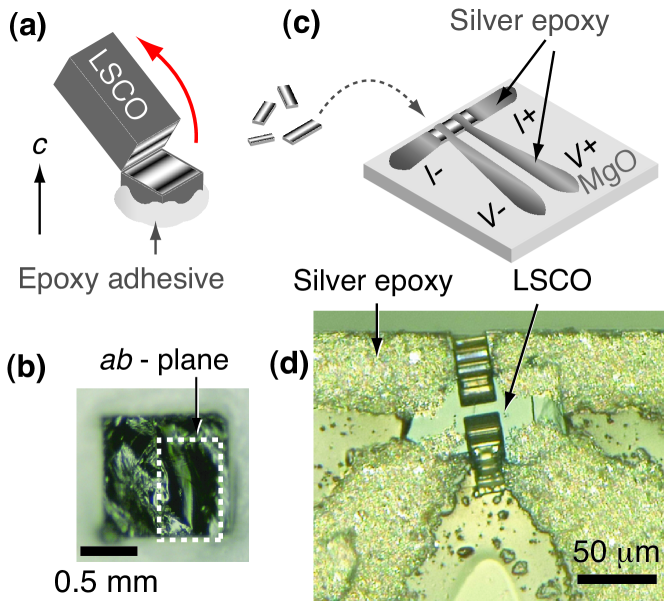
To carve out an -shaped IJJ stack in an LSCO single crystal using the FIB etching techniqueKim:SST1999 , we need to prepare a specimen which is thin along the -axis. The desired thickness is 30 m, because of the slow etch rate of the FIB systemFIB . Figure 1 shows the process to prepare thin LSCO specimens. An LSCO single crystal grown by the traveling solvent floating zone method Tanaka:N1989 , with nominal Sr concentration 0.09, was cut and formed into a small rectangular parallelepiped shape. The dimensions are about 1 1 3 mm3, and the long edge is along the -axis [Fig. 1(a)]. The direction of the crystal -axis was determined by X-ray Laue diffraction patterns before cutting.
The small rod was fixed onto a metal plate with epoxy adhesive (Torr Seal, Ideal Vacuum Products), and carefully cleaved as schematically depicted in Fig. 1(a). A shiny flat surface, an indication of the -plane, appeared after cleaving as shown in Fig. 1(b). Tiny crystal pieces were obtained by cutting the flat part using a wire saw. The typical lateral dimension of these pieces is 0.05 - 0.1 mm, and the typical thickness is 20 - 50 m. One of the pieces was fixed on a magnesium oxide (MgO) substrate by polyimide glue, and four electrical contacts were made by silver epoxy as shown in Fig. 1(c) and 1(d). To reduce contact resistance, we annealed the sample at 400 ∘C for 10 minutes in oxygen in a mirror furnace (MILA-3000, Ulvac).
III Fabrication of a Sub-micron LSCO IJJ Stack by FIB Etching
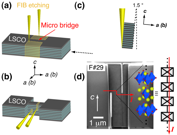
We used a focused a FIB/scanning ion microscope (FIB/SIM) system (SMI-9800SE, Seiko instruments) for both etching and observation. First a constricted micro-bridge was formed in the center of the sample as shown in Fig. 2(a). The length of the bridge is about 5 m and the width is about 1 m. Then we etched the micro-bridge from the direction in order to make two slits, as depicted in Fig. 2(b). The two slits are separated by 0.9 m. Finally the micro-bridge was etched from the direction again, to narrow the width down to 0.5 m. Here the beam angle is slightly ( 1.5∘) tilted to compensate for the finite angle of the ion beam, as schematically shown in Fig. 2(c).
Since the two slits overlap slightly along the -axis, an applied current flows along the direction in-between the slits as shown by the red arrow in Fig. 2(d). Therefore the small area can be regarded as an -shape IJJ stack Kim:SST1999 ; Wang:APL2001 ; You:APL2006 as schematically depicted on the right hand side in Fig. 2(d). The lateral dimension of the LSCO IJJ stack “F#29” is 0.45 0.95 m2. The thickness is about 30 - 40 nm, estimated from SIM images. To our knowledge, this is the first report of a submicron LSCO IJJ stack formed in a bulk crystal.
IV Discussions for F#29
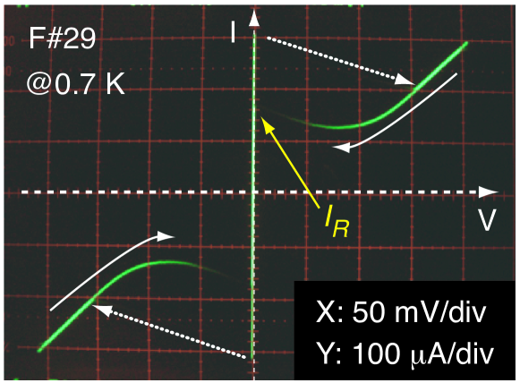
Figure 3 shows a current-voltage () characteristic of F#29 at 0.7 K. A sharp voltage jump (the dashed arrows in Fig. 3) and a large hysteresis (the solid arrows in Fig. 3) are observed. These features suggest that the small structure fabricated acts as a stack of tunnel Josephson junctions, similar to BSCCO IJJ stacksKleiner:PRB1994 ; Wang:APL2001 . Therefore F#29 can be regarded as a submicron LSCO IJJ stack.
Resistive multi-branchesKleiner:PRB1994 do not appear in F#29. On the contrary, we recognize that all the junctions simultaneously switch to their resistive state (dotted arrows in Fig. 3). This fact implies that all the IJJs have the same critical currents; therefore our LSCO crystal has homogeneous carrier density, and the LSCO IJJ stack was fabricated without any extra damage such as residual gallium ions. A similar switching phenomenon has been already reported in uniform BSCCO stacks, and referred to as “uniformly switching” by Jin et al. Jin:PRL2006 . As the great enhancement of the MQT rate proportional to (: the number of stacked IJJs) was observed in the BSCCO uniform stacksJin:PRL2006 , the unconventional and interesting quantum phenomenon may also emerge in LSCO IJJ stacks.
Another feature of F#29 is the large retrapping current (see the arrow in Fig. 3). In underdamped JJ’s, the fluctuation free retrapping current is given by Krasnov:PRB2007
| (1) |
where is the fluctuation free critical current, and is the quality factor of the junction. From Eq. 1 and Fig. 3, of F#29 is roughly estimated to be 3 - 4. This means that the LSCO IJJ stack is moderately damped. Discussing about the damping effect in the LSCO IJJ stack here is beyond the scope of this article. The damping effects of BSCCO IJJ stacks as well as various types of Josephson junctions have been intensively studied by Krasnov et al Krasnov:PRB2007 .
V Fabrication of an LSCO IJJ Stack By FIB and Argon Ion etching
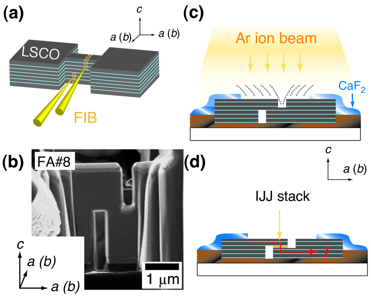
In section III, we described the fabrication process for an LSCO IJJ stack using only FIB etching. A typical spatial resolution of the FIB machine, however, is about 10 - 50 nm. This is rather coarse with respect to the thickness of a single IJJ of LSCO, 0.7 nm. Therefore it is extremely difficult to control using the FIB machine. Because of the new quantum phenomenon mentioned earlierJin:PRL2006 , controlling of an LSCO IJJ stack is an interesting although difficult challenge. Here, we present a developed fabrication method in which argon ion etching is performed after FIB etching in order to gradually increase the thickness of the LSCO IJJ stack.
After making a micro bridge with 0.7 m width by the same procedure described in section III and Fig. 2(a), calcium fluoride (CaF2) was evaporated through a metal mask in order to make a protection layer for the electrodes. Then two slits were formed by FIB etching as schematically depicted in Fig. 4(a). In Fig. 4(b) we show a SIM image of the sample “FA#8” taken after the process of Fig. 4(a). The distance between the slits is 0.5 m. Note that the two slits do not overlap along the -axis, i.e., the IJJ stack is not yet formed at this point. In the next step, the depth of the top slit was gradually increased using an argon ion etching machine (MPS-3000, Ion tech) as schematically shown in Fig. 4(c). As a result, a submicron LSCO IJJ stack with small is formed as depicted in the center of Fig. 4(d).
VI Discussions for FA#8
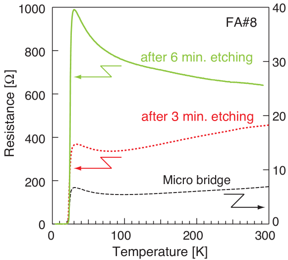
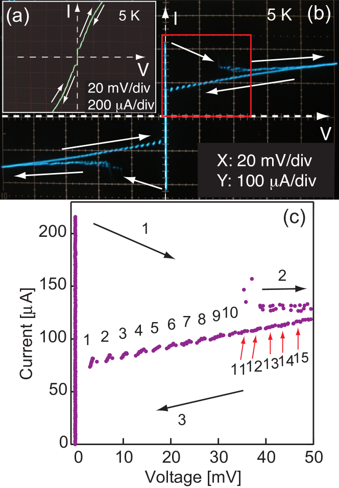
The resistance versus temperature ( - ) curves of FA#8 are shown in Fig. 5. The black dashed curve in Fig. 5 represents the resistance of the micro bridge before making the two slits, as in Fig. 2(a). The red dotted curve in Fig. 5 shows the resistance after making the two slits and 3 min of argon ion etching [see Fig. 4(c)]. One can see that the resistance drastically increases. Figure 6(a) represents the characteristic at this point. A tiny voltage jump without hysteresis, which is similar to a weak-link junction, appears. This implies that the LSCO IJJ stack starts being formed, but at this point the thickness is almost zero. The green solid curve in Fig. 5 is after three more min etching (6 min total). The resistance increases further, and the - curve becomes semiconductive above the superconducting transition temperature. Figure 6(b) and (c) show the curves after etching for 6 min total. Resistive multi-branches emerge, and these are quite distinguishable, especially in the low voltage regime of 0 to 30 mV as indexed in Fig. 6(c). These results both the curves and the curves suggest that the depth of the upper slit has increased along the -axis by the argon ion etching and eventually an LSCO IJJ stack is formed as schematically depicted in Fig. 4(c).
The superconducting transition temperature in Fig. 5 is recognized to be 24 K, which is taken from the mid-points of the transitions. The Sr concentration of FA#8 is thus estimated to be 0.09Takagi:PRB1989 , and is consistent with the nominal value. We note that of all three curves does not change, implying that argon ion etching does not affect the carrier density of the crystal. This is a great advantage for iterative experiments, such as in Ref. You:APL2006 , as well as for applications.
In Fig. 6(c), we determine that is about 15. At higer voltage, the gaps between each resistive brach are narrower. This is probably attributed to self-heating of each LSCO IJJ, as is the case for BSCCO. Assuming , we roughly estimate the etching rate of our argon ion etching machine to be about 3.5 nm/min. With proper values of the acceleration voltage and ion beam current, we should be able to etch LSCO crystals with an etch rate of 0.7 nm/min, namely 1 IJJ/min, as already demonstrated for BSCCO by You et al.You:APL2006 . Thus this method may let us control of an LSCO IJJ stack with an accuracy of single IJJ.
It is interesting that the resistive multi branches are not observed when ramping up the bias current, but observed only while ramping down, as we can see in Fig. 6(b) and (c). After switching [arrow 1 in Fig. 6(c)], the IJJ stack jumps to around 40 mV and goes up to the maximal voltage ( 100 mV) with chaotic behavior [arrow 2 in Fig. 6(c)]. Then it goes down to the superconducting state while showing multi-branches [arrow 3 in Fig. 6(c)]. We have already reported a similar feature of characteristics in a larger ( 3 m2) LSCO IJJ stackKubo:PC2008 , and this phenomenon may be attributed to the strong interaction among stacked IJJsMachida:PRB2004 . Further studies are needed to understand this.
VII Conclusions
In conclusion, we successfully fabricated submicron La2-xSrxCuO4 (LSCO) intrinsic Josephson junction (IJJ) stacks either by focused ion beam (FIB) etching or by an original combined FIB/argon ion beam etching technique. To our knowledge, this is the first demonstration of submicron LSCO IJJ stacks. About 15 resistive multi-branches appeared in the sample fabricated by the latter technique. This method may let us control the number of stacked LSCO IJJs with an accuracy of a single IJJ. This method could also be applied to other cuprate materials which are difficult to cleave with Scotch tape, such as rare earth compounds REBa2Cu3O7-y (RE: rare earth) as well as other Lanthanum compounds.
Acknowledgements.
This work was partially supported by MEXT under Grant No. 1905014. The authors thank M. Tachiki and H. Itozaki for the use of the ion etching equipment, K. Takahashi for the help for the machine maintenance, and M. Nagao for discussions. Y.K. appreciates Ç. Girit for English correction. Y.K. was financially supported by NIMS.References
- (1) R. Kleiner and P. Müller, Phys. Rev. B 49 1327 (1994).
- (2) K. Inomata, S. Sato, K. Nakajima, A. Tanaka, Y. Takano, H. B. Wang, M. Nagao, H. Hatano, and S. Kawabata, Phys. Rev. Lett. 95 107005 (2005).
- (3) X.Y. Jin, J. Lisenfeld, Y. Koval, A. Lukashenko, A.V. Ustinov, and P. Muller, Phys. Rev. Lett. 96 177003 (2006).
- (4) S.-X. Li, W. Qiu, S. Han, Y. F. Wei, X. B. Zhu, C. Z. Gu, S. P. Zhao, and H. B. Wang, Phys. Rev. Lett. 99 037002 (2007).
- (5) H. Kashiwaya, T. Matsumoto, H. Shibata, S. Kashiwaya, H. Eisaki, Y. Yoshida, S. Kawabata, and Y. Tanaka, J. Phys. Soc. Jpn. 77 104708 (2008).
- (6) K. Ota, K. Hamada, R. Takemura, M. Ohmaki, T. Machi, K. Tanabe, M. Suzuki, A. Maeda, and H. Kitano, Phys. Rev. B 79 134505 (2009).
- (7) S. Ueda, T. Yamaguchi, Y. Kubo, S. Tsuda, Y. Takano, J. Shimoyama, and K. Kishio, J. Appl. Phys. 106 074516 (2009).
- (8) Y. Kubo, Y. Takahide, S. Ueda, Y. Takano, and Y. Ootuka, Appl. Phys. Exp. 3 063104 (2010).
- (9) S. Kawabata, S. Kashiwaya, Y. Asano, and Y. Tanaka, Phys. Rev. B 75 014502 (2004).
- (10) T. Yokoyama, S. Kawabata, T. Kato, and Y. Tanaka, Phys. Rev. B 76 134501 (2007).
- (11) M. Machida and T. Koyama, Supercond. Sci. Technol. 20 S23 (2007).
- (12) T. Koyama and M. Machida, Physica C 468 695 (2008).
- (13) S. Savel’ev, A.O. Sboychakov, A. L. Rakhmanov, and F. Nori, Phys. Rev. B 77 014509 (2008).
- (14) S.-J. Kim, Y. I. Latyshev, and T. Yamashita, Supercond. Sci. Technol. 12 729 (1999).
- (15) H.B. Wang, P.H. Wu, and T. Yamashita, Appl. Phys. Lett. 78 4010 (2001).
- (16) L.X. You, M. Torstensson, A. Yurgens, D. Winkler, C.T. Lin, and B. Liang, Appl. Phys. Lett. 88 222501 (2006).
- (17) K. Tamasaku, Y. Nakamura, and S. Uchida, Phys. Rev. Lett. 69 1455 (1992).
- (18) S. Uchida and K. Tamasaku, Phys. Rev. B 53 14558 (1996).
- (19) J. M. Martinis, M. H. Devoret, and J. Clarke, Phys. Rev. B 35 4682 (1987).
- (20) A. Wallraff, A. Lukashenko, C. Coqui, A. Kemp, T. Duty, and A. V. Ustinov, Rev. Sci. Instrum. 74 3740 (2003).
- (21) Y. Uematsu, et al., Physica C 362 290 (2001).
- (22) S.-J. Kim, et al., IEEE Trans. Appl. Supercond. 15 3782 (2005).
- (23) Y. Kubo, T. Tanaka, Y. Takahide, S. Ueda, T. Okutsu, A.T.M.N. Islam, I. Tanaka, and Y. Takano: Physica C 468 1922 (2008).
- (24) H. Kitano, K. Ota, K. Ishikawa, M. Itoi, Y. Imai, and A. Maeda, Physica C 470, S838 (2010).
- (25) Y. Mizugaki, Y. Uematsu, S.-J. Kim, J. Chen, K. Nakajima, T. Yamashita, H. Sato, and M. Naito, J. Appl. Phys. 94 2534 (2003).
- (26) K. Ota, Ph. D thesis, The University of Tokyo, 2009.
- (27) In our system, the etch rate is roughly estimated to be 2 m/min for 100 m2 area of LSCO with the highest emission current mode. Needless to say, the etch rate becomes much slower with lower emission current mode which is needed to form a fine 3D structure such as a submicron IJJ stack.
- (28) I. Tanaka and H. Kojima, Nature (London) 337 21 (1989).
- (29) V. M. Krasnov, T. Golod, T. Bauch, and P. Delsing, Phys. Rev. B 76 224517 (2007).
- (30) H. Takagi, T. Ido, S. Ishibashi, M. Uota, S. Uchida, and Y. Tokura, Phys. Rev. B 40 2254 (1989).
- (31) M. Machida and T. Koyama, Phys. Rev. B 70 024523 (2004).