Tunneling Spectroscopy of Graphene-Boron Nitride Heterostructures
Abstract
We report on the fabrication and measurement of a graphene tunnel junction using hexagonal-boron nitride as a tunnel barrier between graphene and a metal gate. The tunneling behavior into graphene is altered by the interactions with phonons and the presence of disorder. We extract properties of graphene and observe multiple phonon-enhanced tunneling thresholds. Finally, differences in the measured properties of two devices are used to shed light on mutually-contrasting previous results of scanning tunneling microscopy in graphene.
The probability for an electron to tunnel through a very thin potential barrier depends strongly on the number of available states in the target material at the same energy. Tunneling spectroscopy uses this principle to directly probe the density of states of complex materials whose electronic properties are still poorly understood TunnelReview . Furthermore, the phonon energy spectrum of a material can be determined by measuring the second derivative of the tunneling current TunnelReview . Thus, a tunneling measurement can obtain information on both the electronic and phononic properties of a material.
In particular, tunneling experiments have been performed on graphene, a carbon monolayer with a honeycomb lattice where electrons are confined in two dimensions. In this material, electrons behave like relativistic particles obeying the Dirac equation, leading to a variety of exciting electronic behaviors CastroNeto09 . In addition to probing the density of states, prior tunneling spectroscopy measurements on graphene revealed features associated with interactions between electrons, phonons and disorder Zhang08 ; Zhang09 ; Jung11 ; Malec11 . At low carrier densities, charge inhomogeneities modify electron tunneling in scanning tunneling microscopy (STM) Zhang09 ; Jung11 . However, STM experiments have exhibited conflicting results. While some STM measurements have shown a strong suppression of tunneling at low energies Zhang08 ; Brar07 , attributed to interactions between electrons and K-point phonons in graphene Wehling08 , other experiments have not observed this effect, whether for graphene on Jung11 ; Li09 or graphene on hexagonal-boron nitride (h-BN) Xue11 .
In this Letter, we complement the existing tunneling experiments by fabricating graphene tunnel junctions using h-BN as a tunneling barrier. We focus on two devices, referred to below as A and B. The devices were fabricated by the same process, but as we will see below they exhibit different tunnel behavior: one dominated by the density of states in graphene and one dominated by the energy dependence of the transmission probability. Each resembles a different set of prior STM experiments. Properties of graphene extracted from the tunnel measurements, such as disorder-induced charge puddle size and Fermi velocity, agree well with previously reported results obtained via STM. In addition, we observe a rich electron-phonon interaction structure in the inelastic tunneling current, allowing for the identification of resonances near the phonon energies at the K and M-point in graphene as well as two low energy resonances that we attribute to Van Hove singularities in the h-BN phonon density of states. Finally, the energy dependence of the tunnel transmission is strongly influenced by the microscopic details of the device geometry, shedding light on previously mutually-contrasting results in STM experiments.
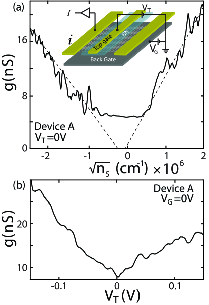
The use of h-BN as an insulating substrate has allowed for high-mobility graphene devices to be fabricated Dean10 . We exfoliate h-BN and graphene on separate degenerately-doped silicon wafer pieces capped with thermally-grown, 300 nm-thick . The thicknesses of the h-BN flakes used are measured with AFM to be 2 nm. After annealing both flakes in Ar and H2 at 350 ∘C for 4 hours each with flow rates of 500 sccm, the h-BN flakes are coated with a thick PMMA layer and the underlying is etched away with a solution of potassium hydroxide, which lifts off the PMMA with the h-BN attached to it. The PMMA-h-BN membrane is then attached to a micro-manipulator arm, similar to Ref. Dean10 , and transferred on top of the graphene sheet. The PMMA is then dissolved away in acetone. Standard e-beam lithography techniques are employed to electrically contact the graphene with 10 nm/50 nm of Ti/Au and to add a top gate, which serves as a tunnel contact, on top of the h-BN flake [see inset of Fig. 1(a) for a schematic of the completed device].
The differential tunnel conductance , where is the tunnel current, is obtained as a function of the top-gate voltage and backgate voltage using a lock-in measurement with an excitation voltage of 1 mV at 13 Hz. , applied to the degenerately-doped Si wafer, controls the average density of electrons in the sheet of graphene. both modulates directly beneath the top gate and allows for the DC voltage bias dependence of the tunneling process to be probed. All experiments are performed at a temperature of 4.2 K. In-plane transport measurements on the devices show a charge-neutrality point (CNP) of 18(-22) V for device A(B).
A plot of as a function of for device A is shown in Fig. 1(a); here, is controlled by , with grounded. The tunnel conductance is proportional to away from the CNP, as shown by the dashed lines, directly reflecting the V-shaped behavior of the density of states. The variation of the density of states due to the metallic top gate is negligible within the range of TunnelReview , and is expressed as
| (1) |
where is the density of states in graphene, is the Fermi energy and is the energy and bias dependent electron tunneling transmission probability, which decays exponentially with distance and depends on the device geometry SuppInfo . and are given by:
| (2a) | |||
| (2b) | |||
where is the Fermi velocity of electrons. At =0, the tunnel transmission is constant and depends only on the density of states: , as observed in Fig. 1(a). However, the density of states does not reach zero when vanishes but instead flattens out when , due to charged-impurity disorder on the graphene flake DasSarma11 . When becomes as low as the density of impurities, p or n-type charge puddles form around the impurities Martin08 . The slopes of on the p-type and n-type regions differ by 20%, indicating that is 9% lower for electrons than for holes. This asymmetry is consistent with the presence of negatively-charged adsorbates on the sheet of graphene Robinson08 ; Lohmann09 .
The -bias dependence of for =0 is shown in Fig. 1(b). Results for device A show a smooth evolution of with , indicating no or relatively small variation in (), similar to Refs. Jung11 ; Li09 ; Xue11 . In particular, there is no exponential suppression of near zero-bias, as was observed in Refs. Zhang08 ; Brar07 ; Malec11 .
is moderately suppressed around =0 and along a diagonal region [Fig. 2(a), outlined by white dashed lines]. This region corresponds to gate voltages such that is close to the CNP Huard07 ; Williams07 , where the density of states is minimal. The tunnel probe also gates the graphene sheet and the relative back(top) gate capacitances () can be determined by fitting = constant. The slope of this line gives the capacitance ratio , which is lower than the ratio of 150 that one expects from a simple parallel plate capacitor model SuppInfo .
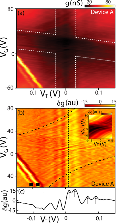
To observe the evolution of fine features in , a derivative with respect to the -axis is taken, resulting in [Fig. 2(b)]. We observe three collections of features in for this range of voltages: peaks moving along parabolas in - space away from the CNP (dashed curves), -independent peaks around =0 (dotted line) and strong features at negative values of and (squares). for sample A is well approximated by SuppInfo , therefore parabolic features in correspond to peaks in the density of states and follow contours of constant . These features can be fit to determine (see SuppInfo for information about the fit), obtaining m/s, in good agreement with the theoretically expected value of m/s Brandt88 . Two very strong diagonal peaks were obtained for between -0.74 V and -0.15 V in the range of between -60 V and 0 V (squares). These two peaks only appear in this device and are not symmetric with respect to the CNP or . While the origin of these two features is not known, it is likely that these are associated with a resonance in an impurity adjacent to the sheet of graphene. A simulation of the tunnel conductance in the presence of disorder is shown in inset of Fig. 2(b), reproducing the features indicated by dashed curves of Fig. 2(b) but not the features labeled by the dotted line or squares (see SuppInfo for details of the simulation). The -independent peaks, highlighted by the dotted line, are most clearly seen in Fig. 2(c) where a cut of that has been averaged over all positive values of is shown. Four peaks are identified by arrows at 10, 32, 68, and 90 mV (accurate to within 1 mV), with the former two peaks appearing stronger than the latter two.
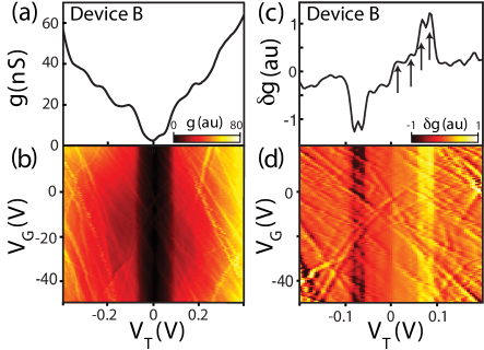
Similar measurements were performed on a second device, B, where primarily depends on and varies only slowly with , a result of the tunnel transmission varying faster than the density of states as a function of . In Fig. 3(a), is suppressed for 70 mV and a dependence characteristic of graphene’s density of states is only observed outside this suppression. The values of where this suppression occured are independent of for the range explored here [Fig. 3(b)]. A plot of for device B [Fig. 3(c)] reveals peaks at similar voltages to those of device A, indicated by arrows at values of 10, 40, 68 and 84 mV (1 mV), but with different intensities than device A. These peaks, like for device A, are independent of [Fig. 3(d)].
Features that are independent of and appear as peaks in can only reflect the variations of the tunnel transmission and not the density of states, and are ascribed to phonon thresholds enhancing tunneling. One such threshold, at 68 mV for device A and B, has been previously measured and assigned to excitations of K-point phonons in graphene Zhang08 ; Brar07 . The three other peaks are previously unreported in graphene tunneling experiments. The lower inelastic thresholds of 10 and 40 mV do not correspond to any phonon energy in graphite Mohr and are likely scattering of tunneling electrons from phonons in h-BN. The phonon spectrum in h-BN exhibits a very flat ZA branch at 40 meV along the MK direction Taniguchi07 . This should be associated with a Van-Hove singularity (VHS) in the phonon density of states at 40meV, explaining why an inelastic threshold is observed at this energy. The 10 mV threshold is attributed to the ZA phonon at the A point Taniguchi07 , where a band flattening is also observed. The highest voltage kink (at 84 mV and 90 mV respectively on device A and B) is close in energy to both the M-point phonon in graphene Mohr and another VHS in the h-BN phonon density of states Taniguchi07 . We also observe that peaks associated with h-BN phonons are much stronger for device A, whereas in device B, the graphene phonon thresholds are the strongest.
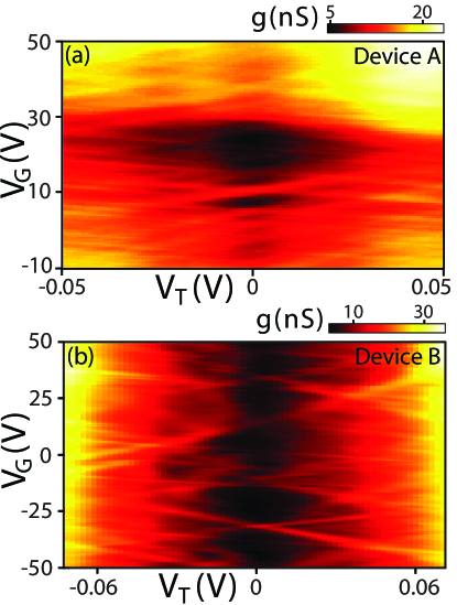
The behavior of at low provides information on the role of impurities in the tunnel transmission (Fig. 4). Both devices exhibit Coulomb diamonds. Similar features have been found in STM experiments Zhang09 ; Jung11 and are due to the formation of charge puddles around charged impurities. These puddles behave like leaky quantum dots and dominate transport in graphene at low density DasSarma11 . For device A, these Coulomb diamonds have different sizes, indicating that several charge puddles are involved. The number and size of these diamonds increase closer to the CNP, which is due to weaker screening of charged impurities Zhang09 . The periodicity of the conductance oscillations as a function of for device A is used to extract the average capacitance of the dots to the back gate, resulting in a typical dot size 200 nm2 (see SuppInfo for details of the dot size extraction), in good agreement with values reported in Ref. Zhang09 . For device B [Fig. 4(b)], the Coulomb blockade features are much more pronounced, indicating that only a few charge puddles are involved. A charging energy of 6 meV and a capacitance to the back-gate of F are measured, which corresponds to a dot size of approximately 70 nm2 SuppInfo , smaller than that of device A. The ratio for device B is found to be 100 SuppInfo , larger than what was found for device A, which indicates that the tunnel gate is closer to the graphene sheet in device B. Given the exponential dependence of the tunnel current on the barrier thickness, one would expect the average value of to be much higher for device B since the capacitance ratio is larger. This is not the case. This difference cannot be accounted for by the top gate geometry either, as the area of the top-gates for the two devices are comparable. This suggests that the tunneling area is much smaller for device B, indicating that tunneling occurs primarily at a very localized point or collection of points. This localized tunneling can result from an impurity trapped between the h-BN and the graphene, locally enhancing the tunneling rate. Another scenario resulting in localized tunneling comes from a small imperfection in the h-BN lattice, causing the tunnel barrier to be lower in one small area.
The data from device A and B show that the relative strength of elastic and inelastic tunneling strongly depends on the geometry of the tunnel junction since only B exhibits a strong suppression of at small values of [Figs. 3(a, b)]. To our knowledge, the phonon-enhanced tunneling effect has only been observed in STM experiments where the tips were prepared to be atomically sharp (see the supplementary infomation of Ref. Zhang08 ). This suggests that inelastic scattering plays a more important role when the tip wavefunction is spatially localized, and therefore has a very broad momentum distribution. h-BN enables us to observe tunneling across a two-dimensional interface: the tunneling electrons have a well-defined parallel momentum and inelastic tunneling is suppressed.
This work was supported by the Center on Functional Engineered Nano Architectonics (FENA), the W. M. Keck fondation and the Stanford Center for Probing the Nanoscale (CPN) . We thank H. C. Manoharan for valuable discussions.
References
- (1) R. Wiesendanger, in Scanning Probe Microscopy and Spectroscopy: Methods and applications(Cambridge University Press, 1998)
- (2) A. H. Castro Neto et al., Rev. Mod. Phys. 81, 109 (2009)
- (3) Y. Zhang et al., Nature Phys. 4, 627 (2008).
- (4) Y. Zhang et al., Nature Phys. 5, 722 (2009).
- (5) S. Jung et al., Nature Phys. 7, 245 (2011).
- (6) V.W. Brar et al., App. Phys. Lett. 91, 122102 (2007).
- (7) C. E. Malec et al., J. of Appl. Phys. 109, 064507 (2011).
- (8) T.O. Wehling et al., Phys. Rev. Lett. 101, 216803 (2008).
- (9) G. Li et al., Phys. Rev. Lett. 102, 176804 (2009).
- (10) J. Xue et al., Nature Mat. 10, 282 (2011).
- (11) C. R. Dean et al., Nature Nano. 5, 722 (2010).
- (12) See Supplementary Info.
- (13) S. Das Sarma, S. Adam, E. H. Hwang, and E. Rossi, Rev. Mod. Phys. 83, 407 (2011).
- (14) J. Martin et al., Nat. Phys. 4, 144 (2008).
- (15) J. P. Robinson, H. Schomerus, L. Oroszlány and V. I. Fal’ko, Phys. Rev. Lett. 101, 196803 (2008).
- (16) L. T. Lohmann, K. von Klitzing, and J. H. Smet, Nano Lett. 9, 1973 (2009).
- (17) N. B. Brandt, S. M. Chudinov and Y. G. Ponomarev, Semimetals 1, Graphite and Its Compounds, North-Holland, Amsterdam (1988).
- (18) B. Huard et al., Phys. Rev. Lett. 98, 236803 (2007).
- (19) J. R. Williams, L. DiCarlo and C. M. Marcus, Science 317, 638 (2007).
- (20) M. Mohr et al. Phys. Rev. B 76, 035439 (2007)
- (21) J. Serrano et al. Phys. Rev. Lett. 98, 095503 (2007).
- (22) X. Blase et al. Phys. Rev. B 51 6868 (1995)