Determination of the graphene growth mode on SiC(0001) and SiC(0001̄)
Abstract
We have determined the growth mode of graphene on SiC(0001) and SiC(0001̄) using ultra-thin, isotopically-labeled Si13C ‘marker layers’ grown epitaxially on the Si12C surfaces. Few-layer graphene overlayers were formed via thermal decomposition at elevated temperature. For both surface terminations (Si-face and C-face), we find that the 13C is located mainly in the outermost graphene layers, indicating that, during decomposition, new graphene layers form underneath existing ones.
pacs:
68.65.Pq, 81.05.ue, 68.37.Nq, 61.05.NpGraphene has attracted considerable attention, in part, due to potential applications in electronics Novoselov et al. (2005); Zhang et al. (2005); Berger et al. (2006). Several techniques have been employed to synthesize graphene: mechanical exfoliation, chemical vapor deposition onto metal surfaces, and sublimation of Si from SiC. This latter technique is attractive for electronics application because the graphene is formed directly on an insulating substrate, although many aspects of the formation process are poorly understood. Graphene has been grown via decomposition on several polytypes of SiC. Attention has mainly focussed on the (0001) and (0001̄) surfaces of the 4H and 6H polytypes. These polytypes correspond to different stacking sequences of hexagonal SiC bilayers. Within the bilayers, Si and C atoms are not co-planar. At the (0001) surface, the Si atoms are outermost, while at the (0001̄) surface, the C atoms are outermost.
Perhaps surprisingly, the growth of graphene on these two surfaces is significantly different. On SiC(0001), graphene layers are epitaxial, forming a well-ordered superstructure Forbeaux et al. (1998). Even thick graphene films exhibit an epitaxial relationship to the underlying substrate. In contrast, graphene grown on SiC(0001̄) is more randomly oriented, indicating a much weaker substrate influence Hass et al. (2006, 2008).
These differences in graphene crystallography suggest that the growth mode of graphene might be very different on these surfaces. On SiC(0001), the observed epitaxy has led to speculation that graphene grows “from the inside out” Emtsev et al. (2008). That is, strong coupling to the substrate induces epitaxy in the first graphene layer. The second graphene layer forms under the first, and is oriented due to coupling to the SiC. The second layer displaces the first layer outward. This process continues as the film grows thicker, resulting in a crystalline film in which the outmost layer is the first layer to form. The more-random stacking of graphene on SiC(0001̄) makes it difficult to infer the growth mode, but might indicate that it is substantially different from SiC(0001).
Here, we use isotopic labeling to directly measure the graphene growth mode on both SiC(0001) and SiC(0001̄). We grew ultra-thin epitaxial SiC layers via chemical vapor deposition using a mixture of disilane and isotopically pure 13C ethylene. The thickness of the epitaxial layers was 4-5 bilayers, so that the carbon content was slightly more that that of a single graphene layer. We then formed graphene via SiC decomposition at elevated temperature van Bommel et al. (1975); Forbeaux et al. (1998). After graphene formation we used medium-energy ion scattering (MEIS) van der Veen (1985) to measure the depth distributions of both 12C and 13C. If graphene grows from the inside out 13C will be located predominantly at the surface. Conversely, if new graphene layers form on top of existing ones, 13C will be situated underneath a 12C overlayer. We found that for graphene grown on both SiC(0001) and SiC(0001̄), 13C remains largely at the surface, showing directly that new graphene layers form under existing layers.
Our approach is similar to that used by Gusev et al. to study the oxidation of Si(001) using 16O2 and 18O2 Gusev et al. (1995). In that work the authors carried out a two-step oxidation of Si(100) at elevated temperature, e.g. first using 18O2, and then using 16O2. They then used MEIS to measure the depth profile of 18O and 16O. From this data they determined the growth mode of SiO2 on Si(100) for different processing conditions. For example, they found that at 900C, SiO2 growth beyond 4-5 nm occurs mainly by diffusion of oxygen from the gas phase through the oxide to the Si interface Gusev et al. (1995).
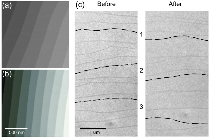
SiC(0001)-6H and (0001̄)-6H surfaces were prepared by degassing for several hours in vacuum at 700C. Oxygen contamination was removed by annealing at 900C in a background pressure of Torr dislane for 5 minutes. After cleaning, the sample temperature was raised to 1200C for 10 minutes in the disilane. As described elsewhere Tromp and Hannon (2009), the disilane prevents the formation of graphene. Prolonged annealing at 1200C leads to the formation of a uniform, reproducible surface that consists of terraces bounded by straight steps with a uniform step height of 0.8 nm (Fig. 1). This step height corresponds to three SiC bilayers.
For the Si-face, electron diffraction analysis Sun et al. (2011) and first-principles modeling Hannon et al. (2009) shows that triple-height steps are characteristic of the lowest-energy surface configuration for the 6H polytype.
Isotopically-labeled, epitaxial SiC layers were then grown by exposing the clean surface to a mixture of disilane (Si2H6) and isotopically-pure ethylene (13C2H4). In this way, SiC bilayers containing 13C, i.e. Si13C, were grown on top of the Si12C substrate. Prior to ethylene exposure, the substrate temperature was raised to 1200C in Torr disilane. The growth of Si13C was initiated by adding 13C2H4 to the disilane until a total pressure of Torr was achieved. The growth of epitaxial layers was monitored in situ using LEEM. Under these growth conditions, and for terraces widths of a few 100 nm, Si13C grows via step-flow, with three bilayers advancing simultaneously. That is, the step height of 0.76 nm is maintained. During growth, steps advanced at a constant rate, and the nucleation of new SiC layers (e.g. islands) was not observed. LEEM images recorded before and after Si13C growth are shown in Fig. 1c. The positions of selected steps are marked before and after growth, indicating that slightly more than three bilayers of SiC were grown.
The measured step velocity corresponded to a growth rate of approximately one SiC bilayer per minute. After the growth of about three SiC bilayers, the ethylene flow was stopped, but the disilane background pressure was maintained in order to prevent graphene formation. When the ethylene was removed, the step motion ceased. The structure of the resulting surface is shown schematically in Fig. 2a. Each bilayer consists of a 50/50 mixture of Si and C. At the (0001) surface, the Si atoms are displaced outward relative to the C atoms. The reverse is true at the (0001̄) surface.
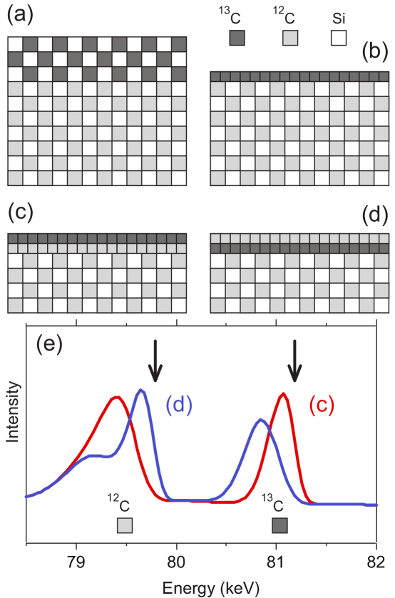
The structure shown in Fig. 2a corresponds to three Si13C bilayers grown on bulk Si12C. When annealed above the Si sublimation temperature, graphene will form. The 6H polytype decomposes in units of three bilayers Hannon and Tromp (2008), and the carbon density in graphene is equal to that of three bilayers. Therefore, the structure shown in Fig. 2b – a pure 13C graphene layer on bulk Si12C – should result if the decomposition is halted after the formation of a single graphene layer. This ‘marker’ layer can be used to determine where additional graphene layers form, giving insight into the kinetics of graphene formation. For example, if additional graphene layers form under pre-existing layers (Fig. 2c), the 13C layer will always be outermost. Conversely, if additional layers form on top of pre-existing graphene, the 13C layer will be located at the graphene/SiC interface, underneath a 12C graphene overlayer (Fig. 2d).
MEIS can be used to distinguish between these two possible growth modes. In our MEIS experiments, a 100 keV proton beam was incident normal to the surface and the kinetic energy of the backscattered protons was measured over a range of scattering angles near 110∘. The energy of the backscattered protons can be used to determine the depth distribution and mass of the near-surface atoms. Two basic processes determine the final proton energy. First, when a proton scatters elastically from a nucleus, conservation of energy and momentum leads to a characteristic backscatter energy given by the mass of the target nucleus and the scattering angle. This dependence can be used to measure the absolute concentrations of 12C and 13C. Each isotope gives rise to a characteristic peak in the proton energy spectrum. Second, as the proton travels through the sample, inelastic electronic interactions give rise to a characteristic energy loss per unit length travelled. For most materials, the maximum energy loss per unit length (for protons) occurs near 100 keV, which makes MEIS particularly surface sensitive. Protons that scatter from nuclei located below the surface will have a lower kinetic energy than those that scatter from nuclei at the surface. The depth distribution will give a characteristic shape and width to the peak in the proton energy spectrum. These features of MEIS make it possible to measure accurate depth profiles for both 12C and 13C Copel et al. (2011).
In Fig. 2e the calculated energy distribution of scattered protons is shown for the structures indicated in Fig. 2c,d. The simulation is for an incident energy of 100 keV, with a total instrumental resolution of 150 eV, and a scattering angle of 110∘. Both distributions have two clear peaks, associated with the two carbon isotopes. The proton energy is higher for 13C than for 12C simply because the target nucleus is heavier. Arrows indicate the kinetic energy of protons that scatter from 12C and 13C at the surface (the ‘surface channel’). The 13C peak for model (d) is lower in energy than that for model (c), reflecting the fact that the 13C graphene layer in (d) is underneath a 12C overlayer. In addition, the 12C peak for model (d) has two components. The larger peak, close to 80 keV, is due to scattering from the 12C graphene layer at the surface, while the broader peak at lower energy is due scattering from carbon in SiC.
LEEM imaging during Si13C epitaxy shows that the structure depicted in Fig. 2a can be grown on both SiC(0001) and SiC(0001̄). After epi-layer growth, monolayer (ML) graphene layers (Fig. 2b) were formed by raising the temperature to 1270C and slowly reducing the background pressure of disilane while the surface was imaged Tromp and Hannon (2009). When a complete layer graphene formed, the sample temperature was quickly reduced to prevent further decomposition. After graphene formation, the samples were transferred (through air) to the MEIS system.
Selected data from graphene layers grown on both SiC(0001) and SiC(0001) are shown in Fig. 3. The filled symbols in Fig. 3a correspond to a sample with 1.3 ML of graphene. A convenient parameterization of the 13C content is given by , where and are the numbers of 12C and 13C atoms in the volume of interest. For the graphene film , indicating small but significant intermixing during decomposition at 1270C. Most likely, 12C is incorporated in the graphene due to the formation of pits during the decomposition Hannon and Tromp (2008). Pits expose the underlying SiC, which can then decompose and contribute 12C to the graphene layer. The presence of some 12C in the graphene layer can also result from imperfect ‘reverse’ step flow during decomposition. If the final step structure is not identical to the structure before Si13C growth (e.g. Fig. 1c), some Si13C will remain and some Si12C will decompose, contributing 12C to the graphene.
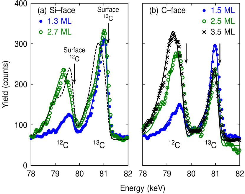
Thicker graphene films were produced using a two-step process. First, 13C-rich graphene monolayers were formed using the method described above: growth of about three bilayers of epitaxial Si13C at 1200C followed by controlled decomposition at 1270C to form the initial graphene layer. Next, additional graphene layers were formed by annealing for 3’ at 1450C. MEIS analysis of these films shows that the graphene film is indeed thicker. For example, for the film shown in (Fig. 3a, open symbols), the graphene thickness was 2.7 layers (with the equivalent of 1.7 layers of 13C and 1.0 layer of 12C). The qualitative result is clear in the raw data shown in Fig. 3a. Compared to the 1.3 ML film, the 12C peak for the 2.7 ML film is larger, and the centroid is shifted to lower energy. The shift to lower energy indicates that the bulk of the 12C graphene is located further from the surface. The 13C peak has roughly the same intensity and is not shifted in energy. These observations suggest that the thicker film contains more 12C graphene, but that the additional graphene is located below the surface. Quantitative analysis supports this conclusion: the top half of the film is 13C-rich () while the lower half is 12C-rich (). This direct measurement shows that the growth mode of graphene on SiC(0001) corresponds to Fig. 2c. New graphene layers form underneath pre-exisiting layers, as proposed by Emtsev et al. Emtsev et al. (2008). In addition, the MEIS analysis shows that there is very little bulk C diffusion during the brief (minutes) annealing at 1450C. Finally, the black dashed line in Fig. 3a shows the simulated spectrum for a graphene film with an inverted isotope depth distribution: 12C-rich in the top half () and 13C-rich in the lower half (). The disagreement with the measured data is striking, indicating the sensitivity of the MEIS analysis to the isotopic composition.
On the SiC(0001̄) surface, graphene growth would appear to be quite different. In contrast to SiC(0001), graphene grown the C-face is not locked azimuthally to the substrate. The domains size measured in our experiments is generally smaller, and both the graphene growth rate and nucleation rate are significantly higher than on SiC(0001). We performed MEIS experiments in order to determine if the growth mode is fundamentally different from that measured for SiC(0001).
Graphene layers of varying thickness were formed on SiC(0001̄) using a similar procedure to that described above for SiC(0001). The only significant difference was that, due to the higher growth rate on SiC(0001̄), thicker graphene films were formed at 1325C rather than 1450C. The MEIS analysis of 1.5, 2.5 and 3.5 ML films is shown in Fig. 3b. In all cases, the thickness of the epitaxial Si13C layer intially grown corresponded to about 1.4 ML of graphene. For the 1.5 ML film, 3/4 of the 13C remained in the graphene layer (), indicating that the intermixing during the initial graphene formation is similar to what was observed for SiC(0001). For the thicker films, several qualitative observations can be made. First, the area of the 12C peak clearly increases with annealing time, indicating more graphene. Conversely, the area of the 13C is essentially constant (within the sample-to-sample variation in the Si13C thickness). Furthermore, the 13C peak does not shift to lower energy, indicating that, in all cases, the 13C graphene is located mainly at the surface. Quantitative modeling confirms this view. For the 2.5 ML film, in the top half of the film, while in the lower half, . Clearly most of the 13C remains at the surface. For the 3.5 ML the results are similar: in the top third of the film, while in the bottom 2/3 of the graphene film. Taken together, these results show that when SiC(0001̄) is annealed at 1325C, additional graphene layers form underneath the initial (13C-rich) graphene layer formed at 1200C. That is, the graphene growth mode is essentially the same on SiC(0001) and SiC(0001̄), despite the stark contrast in the crystal quality of the graphene layers on SiC(0001) and SiC(0001̄).
In summary, we have directly measured the growth mode of graphene on SiC(0001) and SiC(0001̄) during surface decomposition at high-temperature. Ultra-thin Si13C epitaxial ‘marker layers’ were growth on both surfaces. Following graphene formation, MEIS was used to measure the depth distribution of 13C and 12C. At both surfaces (Si-face and C-face), we find that 13C is located primarily in the outmost graphene layers. That is, despite very different graphene crystallography on the (0001) and (0001̄) surfaces, the graphene growth mode is the same: new graphene layers form underneath existing ones.
This work was supported by DARPA under Contract No. FA8650 08-C-7838 through the CERA program.
References
- Novoselov et al. (2005) K. S. Novoselov, A. K. Geim, S. V. Morozov, D. Jiang, M. I. Katsnelson, I. V. Grigorieva, S. V. Dubonos, and A. A. Firsov, Nature 438, 197 (2005).
- Zhang et al. (2005) Y. Zhang, Y.-W. Tan, H. L. Stormer, and P. Kim, Nature 438, 201 (2005).
- Berger et al. (2006) C. Berger, Z. Son, X. Li, X. Wu, N. Brown, C. Naud, D. Mayou, T. Li, J. Hass, A. N. Marchenkov, E. H. Conrad, P. N. First, and W. A. de Heer, Science 312, 1191 (2006).
- Forbeaux et al. (1998) I. Forbeaux, J.-M. Themlin, and J.-M. Debever, Phys. Rev. B 58, 16396 (1998).
- Hass et al. (2006) J. Hass, R. Feng, T. Li, X. Li, Z. Zong, W. A. de Heer, P. N. First, E. H. Conrad, C. A. Jeffrey, and C. Berger, Applied Physics Letters 89, 143106 (2006).
- Hass et al. (2008) J. Hass, F. Varchon, J. E. Millán-Otoya, M. Sprinkle, N. Sharma, W. A. de Heer, C. Berger, P. N. First, L. Magaud, and E. H. Conrad, Phys. Rev. Lett. 100, 125504 (2008).
- Emtsev et al. (2008) K. V. Emtsev, F. Speck, T. Seyller, L. Ley, and J. D. Riley, Phys. Rev. B 77, 155303 (2008).
- van Bommel et al. (1975) A. van Bommel, J. Crombeen, and A. van Tooren, Surf. Sci. 48, 463 (1975).
- van der Veen (1985) J. F. van der Veen, Surf. Sci. Rep. 5, 199 (1985).
- Gusev et al. (1995) E. P. Gusev, H. C. Lu, T. Gustafsson, and E. Garfunkel, Phys. Rev. B 52, 1759 (1995).
- Tromp and Hannon (2009) R. M. Tromp and J. B. Hannon, Phys. Rev. Lett. 102, 106104 (2009).
- Sun et al. (2011) J. Sun, J. Hannon, R. Tromp, and K. Poh., IBM J. Res. Develop. NA, NA (2011).
- Hannon et al. (2009) J. B. Hannon, R. M. Tromp, N. V. Medhekar, and V. B. Shenoy, Phys. Rev. Lett. 103, 256101 (2009).
- Hannon and Tromp (2008) J. B. Hannon and R. M. Tromp, Phys. Rev. B 77, 241404 (2008).
- Copel et al. (2011) M. Copel, S. Oida, A. Kasry, A. A. Bol, J. B. Hannon, and R. M. Tromp, Applied Physics Letters 98, 113103 (2011).