Detecting Majorana Bound States by Nanomechanics
Abstract
We propose a nanomechanical detection scheme for Majorana bound states, which have been predicted to exist at the edges of a one-dimensional topological superconductor, implemented, for instance, using a semiconducting wire placed on top of an -wave superconductor. The detector makes use of an oscillating electrode, which can be realized using a doubly clamped metallic beam, tunnel coupled to one edge of the topological superconductor. We find that a measurement of the nonlinear differential conductance provides the necessary information to uniquely identify Majorana bound states.
pacs:
85.85.+j, 73.23.-b, 74.45.+c, 71.10.PmI Introduction
Over the past few years, nanomechanics and the field of topological condensed matter systems have been pushing limits in their respective area of research. Nanomechanical systems have proven to be exceptional measurement devices for, e.g., mass, force, and position LaHaye et al. (2004); Lassagne et al. (2009); Mamin and Rugar (2001); Steele et al. (2009); Yang et al. (2006), as well as a unique platform for studying fundamental questions concerning the quantum nature of macroscopic objects, theoretically as well as experimentally Marshall et al. (2003); Schmidt et al. (2010); O’Connell et al. (2010); Teufel et al. (2104).
Majorana fermions are among the most intriguing features of topological states of matter. They are their own anti-particles, i.e., , and satisfy fermionic anticommutation relations . A Majorana fermion has half the degrees of freedom of a Dirac fermion. This can be seen, for instance, by expressing two Majorana fermions as and , where and are the annihilation and creation operators, respectively, of a single Dirac fermion and satisfy . Various proposals have been made about how to generate Majorana states Read and Green (2000); Kitaev (2001); Fu and Kane (2008, 2009a); Sau et al. (2010); Lutchyn et al. (2010); Oreg et al. (2010); Alicea (2010). In view of future applications, these states might be particularly useful in the field of topological quantum computation Nayak et al. (2008). Unfortunately, to date no experimental realization of Majorana fermions has been achieved. Proposed detection schemes are based on tunnel setups Bolech and Demler (2007); Nilsson et al. (2008); Law et al. (2009); Flensberg (2010); Leijnse and Flensberg (2010), interferometer setups Akhmerov et al. (2009); Fu and Kane (2009b); Fu (2010); Béri (2011); Liu and Trauzettel (2011) and the Josephson effect Fu and Kane (2008, 2009a); Lutchyn et al. (2010). However it is fair to say that true qualitative experimental signatures of Majorana fermions that persist in realistic systems are rather difficult to predict.
In this paper, we present a novel scheme for detecting Majorana bound states (MBS) at the edges of topological superconductors. Our proposal involves an oscillating electrode tunnel coupled to a topological superconductor (TS) hosting MBS (see Fig. 1). We show that the interplay between the two weakly coupled MBS, located at the edges of the TS, and the oscillating electrode gives rise to unique features in the differential conductance of the setup. We find that in the presence of the resonator, satellite peaks appear in the differential conductance. We identify the underlying transport processes giving rise to the rich structure in the differential conductance. Furthermore, we study the dependence of the differential conductance on the effective temperature of the oscillator and find for an oscillator close to its quantum mechanical ground state a qualitative transport signature which is due to the interplay between the resonator and the Majorana bound states.
The paper is organized as follows. We introduce the setup under investigation and the underlying model in Sec. II, followed by details on the calculation of the current in the setup in Sec. III. In Sec. IV, we present our results with subsections focusing on a setup with and without the resonator. Finally, we conclude in Sec. V.
II Setup and Model
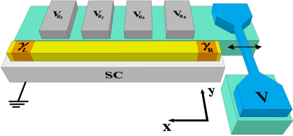
The detection scheme we propose is schematically depicted in Fig. 1. The TS can, for instance, be realized as a semiconducting wire with strong spin-orbit coupling placed on top of an -wave superconductor in the presence of a magnetic field Sau et al. (2010); Lutchyn et al. (2010); Oreg et al. (2010). Its left and right edges host two MBS which we call and . One of the edges, say the right one, is coupled by tunneling to a movable doubly clamped beam. While this setup can be technically challenging to realize, one should note that the fabrication of metallic doubly clamped nanoresonators with very high frequencies and quality factors has been recently reported Flowers-Jacobs et al. (2007); Li et al. (2008). The motion of the beam modulates the tunnel amplitude, such that it depends on the displacement of the beam. The oscillating electrode is held at a bias voltage and the TS is grounded.
We approximate the tunnel amplitude as linear in the displacement of the beam, . This approximation is justified if the oscillation amplitude is small compared to the mean distance between the beam and the edge of the TS. The Hamiltonian of the system is then given by
| (1) |
where describes a spinless electron reservoir in the metallic oscillating electrode. Here, we restrict ourselves to one spin channel only. This is appropriate since the one-dimensional (1D) semiconducting wire on top of an -wave superconductor in the presence of a magnetic field has the same degrees of freedom as a spinless superconductor Fu and Kane (2008); Oreg et al. (2010). In reality, both spins will participate and their signal will add up to the one we calculate below. Furthermore, we assume a linear dispersion . Next, is the usual harmonic oscillator Hamiltonian describing the motion of the beam with an effective mass and resonance frequency . The term characterizes the overlap between the MBS on the left edge and the right edge of the TS Semenoff and Sodano (2007). Describing these two Majorana fermions as one Dirac fermion, we can rewrite . The Hamiltonian is formally identical to that of a single resonant level (RL) at energy . However, due to the nonlocal nature of the MBS, the overlap depends exponentially on the effective length of the TS. This distinguishes the MBS Hamiltonian from a RL. In order to probe the length dependence of , gate electrodes can be installed in proximity to the TS Hassler et al. (2010); Alicea et al. (2011), schematically shown in Fig. 1. Then, by applying gate voltages, the effective length , and thus , can be tuned.
The bare tunnel Hamiltonian has been introduced for a related setup in Ref. Bolech and Demler, 2007 and the -dependent term is new here. Assuming that the tunneling takes place locally at , both are given by
| (2) | ||||
| (3) |
Note that, due to the form of and , the Majorana fermion couples to lead electrons as well as lead holes. We cast Eq. (2) into a form containing Dirac fermions:
and analogously for . We assume that the lead electrons only couple to in and , which is justified if the wire is much longer than the superconducting coherence length of the -wave SC, the characteristic localization length of the MBSFu and Kane (2008).
Since MBS are subgap states, we investigate the regime of a large superconducting gap , i.e., , where is the density of states of the metallic lead.
If the electrode does not oscillate, the system is described by the quadratic Hamiltonian . In this case, all Green’s functions (GF) involving and operators are known exactly. Since does not conserve fermion numbers, the anomalous GF do not vanish, e.g., . Then, nonequilibrium transport properties like the current or the current noise can be determined exactly Bolech and Demler (2007).
III Current calculation
We shall treat the -dependence of the tunneling amplitude as a perturbation to the Hamiltonian . This requires that , where is the amplitude of the zero point fluctuations and the mean phonon number of the resonator. We restrict ourselves to second order perturbation theory in . Our main focus is the calculation of the current. Putting , the current operator is given by , where denotes the number of fermions in the lead. Using the vector notation , we find , where
| (4) | ||||
| (5) |
Here, is a real matrix
| (10) |
We introduce the fermion GF
| (11) |
where and denotes the time ordering operator on the Keldysh contour. Later we will introduce Kelysh indices referring to the lower (time-ordered) and upper (anti-time-ordered) branch of the Keldysh contour, respectively. The average is taken with respect to the ground state of the unperturbed Hamiltonian . For , the time-independent average current can be written as
| (12) |
where
| (13) |
is the Keldysh Green’s function, for which in general we have .
Next, we consider the corrections to this current for small . Using a similar matrix notation allows us to write
| (14) |
with
| (19) |
Introducing the unperturbed oscillator Green’s function
| (20) |
the first order correction to the fermion Green’s function can be expressed as (for )
| (21) |
where and denote the branches of the Keldysh contour.
We express the second-order correction to the GF matrix in terms of the advanced, retarded, and Keldysh components as
| (24) |
where the transformation is given by
| (27) |
This leads to the following compact form of the second-order correction to the GF in the rotated Keldysh space:
| (28) | ||||
where the effects of the oscillator are contained in the self-energy
| (29) | ||||
| (32) |
We will assume that the mechanical oscillator has a very high quality factor, such that the linewidth of the uncoupled oscillator is small compared to the effective linewidth of the fermionic level at . With these assumptions, we can use the following advanced, retarded and Keldysh GF in Fourier space:
| (33) | ||||
| (34) | ||||
| (35) |
with . Finally, the average current including the oscillator can be written as , where is given by Eq. (III) and the two remaining terms are ()
| (36) | ||||
The analytic result for is too long to be displayed here. We demonstrate in the following that the average current contains unique information about the MBS which can be most easily identified in the nonlinear differential conductance .
IV Results
Compared to earlier proposals Bolech and Demler (2007), we have two additional energy scales involved in the detection scheme: the resonance frequency of the oscillator and its effective temperature . Both are to some extent experimentally tunable. Assuming that the oscillator is in a thermal state, one has where is the mean phonon number of the oscillator and where we set . In the following, we will discuss the regime where is small, i.e., comparable to 1. This is challenging to realize experimentally. Note, however, that for the highest resonance frequencies of the doubly clamped beams in Ref. Li et al., 2008 ( MHz), the thermal occupation number could actually become less than 1 at typical dilution refrigerator temperatures. At higher temperatures or lower frequencies, one would have to implement additional cooling schemes to bring the oscillator to the quantum regime. In our model, we make the assumption that the electronic system is at zero temperature, . The side peaks in the differential conductance can be resolved as long as . If the electronic system and the oscillator are in equilibrium with the same heat bath, this translates to the requirement . However, can also be fulfilled for larger if the oscillator is put into an excited state using experimental techniques as, for instance, done in Ref. O’Connell et al., 2010.
IV.1 Reviewing the case without the resonator
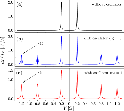
For clarity, let us start with the case without oscillator () and briefly discuss the dependence of the differential conductance on the length of the TS and thus its dependence on . In the case of a finite overlap of the two MBS, the differential conductance shows two peaks at which can be seen in Fig. 2 (a) (see also Ref. Stanescu et al., 2011 for comparison). Both of the peaks have the height Note (1). Importantly, for any finite , at vanishes in our model. This is in stark contrast to the differential conductance in quantum dots coupled to one superconducting and one normal lead Domański and Donabidowicz (2008). Hence, it is rather straightforward to distinguish this situation from the MBS case. As mentioned above, the Hamiltonian is formally equivalent to one describing a spinless resonant level at energy . Therefore, a comparison to a resonant level case is of pedagogical value. Two resonant levels with energies might lead to a similar signal in the differential conductance as in the MBS case. This could, for instance, happen if the magnetic field destroyed the superconductivity in an experimental realization of our proposal. Increasing the effective length of the wire using the gate electrodes, one can tune close to zero, which would yield a single peak at (not shown in Fig. 2). However, this feature in the differential conductance could also be due to a single RL with energy and consequently an ordinary bound state might mistakenly be identified as a MBS. We conclude that tunneling into resonant levels could be hard to distinguish from tunneling into MBS. However, it is fair to say that a measurement of as a function of the variation of the length of the TS could yield a strong signature of MBS, even in the case of static leads. Furthermore, on resonance in the MBS case, which might not be the case for tunneling into a RL. Interestingly, we show below that the oscillating electrode exhibits additional features in the differential conductance, allowing for an unambiguous identification of MBS.
IV.2 Differential conductance including the oscillator
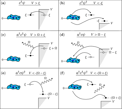
The differential conductance in the presence of the oscillator and its dependence on the oscillator’s temperature is shown in Figs. 2(b) and 2(c) for two temperatures corresponding to and , respectively. Due to the presence of the oscillator, satellite peaks emerge at . In Fig. 3, we depict the energetically allowed tunnel processes for , which explain the emerging satellite peaks in Fig. 2. (Note that for more processes are possible corresponding to the emission of a phonon by the oscillator. These are not shown in Fig. 3.) Evidently, for the conventional processes in Figs. 3(a), 3(c), and 3(e), the superconducting condensate does not play any role. Hence, these processes also matter for tunneling into a RL where the condensate in Fig. 3 would be replaced by a second lead. The processes in Figs. 3(b), 3(d), and 3(f), on the other hand, rely on the presence of the superconducting condensate. Importantly, all processes in Figs. 3(a) to 3(f) contribute together to the rich structure in the shown in Fig. 2. Increasing the oscillator’s temperature leads to an increase in the heights of the satellite peaks and transforms a dip at into a peak. This will be further discussed in Fig. 4.
As mentioned above, one can argue that in a single RL scenario with level energy , the signal in the differential conductance could not be clearly distinguished from the one stemming from MBS. Including the oscillator permits us to unambiguously distinguish the two cases. Figure 4 shows our key result. In that figure, we compare the RL case to the MBS case, both in the presence of an oscillating tunnel contact. For clarity, we focus on a region around the resonant frequency of the oscillator and positive bias voltage . Importantly, an oscillator in its ground state () can only absorb a phonon. In the case of the single RL, the crucial tunnel process near the resonance at (for an oscillator with ) is depicted in the right inset of Fig. 4. We see that this process only sets in for voltages (at zero temperature) since the state in the right lead has to be occupied in order to transfer the energy to the oscillator. As a consequence, the differential conductance is only positive for (shown as a solid black line in Fig. 4). The situation is very different for the MBS case. Here, we have a second crucial tunnel process depicted in the left inset of Fig. 4. Then, the dashed-dotted blue line in Fig. 4 illustrates that, for the oscillator in its ground state and MBS present, the is positive for and . This feature is only due to tunneling through MBS and clearly separates the RL from the MBS scenario. If we gradually increase from zero to one (where only the two extremes are shown in Fig. 4), the dip for in the MBS case transforms smoothly into a peak due to additional processes where the oscillator emits a phonon.
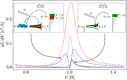
The dip at is due to an interference effect between the two participating tunnel processes which can be understood on the basis of Fermi’s golden rule. To illustrate this, we choose and and write the system Hamiltonian as with
| (37) | ||||
| (38) |
In our initial state, the Fermi sea should be filled up to the chemical potential (measured from ), furthermore the fermionic subgap state is empty and no phonons are present, written as
| (39) |
with energy , being the energy of the filled Fermi sea.
To the lowest order in , the leading contribution to at is generated by a combination of the two tunneling processes and , where one of them is accompanied by the creation of a phonon mode.
The current-carrying transport processes we focus on are mediated by the processes described by in combination with (cf. insets in Fig. 4). For these transport processes the final state lacks two electrons in the Fermi sea (at momenta ), contains one phonon and an unoccupied subgap state , i.e. we have
| (40) |
with energy
| (41) |
where is the single-particle electron energy and the phonon energy is . As usual, the transition amplitude between the states above, up to second order in is given by
| (42) |
and according to Fermi’s golden rule, the rate is given by summing over all final states respecting energy conservation
| (43) |
The rate is proportional to the current, and therefore proportional to the differential conductance. By evaluating the amplitude and the rate , we find that for the above process, the amplitude vanishes for tunneling particles with energy close to . This leads to the conclusion that for the differential conductance vanishes due to an interference effect between the two processes (of order ) generated by the terms and in the tunneling Hamiltonian. This explains the dip in the differential conductance in Fig. 4.
V Conclusion
To conclude, we have presented an idea of coupling Majorana bound states to a sensitive nanoelectromechanical measurement device. We have shown that a setup where an oscillating, doubly clamped beam is tunnel coupled to a topological superconductor gives rise to unique transport signatures based on the interplay between the mechanical excitations and the Majorana bound states. A smoking gun signature of Majorana bound states has been identified for an oscillator close to the quantum ground state which can be achieved by cooling a resonator to . This energy scale is well below the large parameter of our model, i.e. the superconducting gap . When we, for instance, take an wire proximity coupled to an -wave superconductor, the superconducting gap of can induce a superconducting gap of in the wire Lutchyn et al. (2010). Hence, our predictions are in principle observable at dilution refrigerator temperatures.
Acknowledgements.
SW and BT acknowledge financial support from the DFG-JST Research Unit Topological Electronics. TLS acknowledges support from the Swiss National Science Foundation and KB from the Research Council of Norway, FRINAT Grant 191576/V30. We would like to thank Jan Budich, Matthew Gilbert, Taylor Hughes, and Ronny Thomale for interesting discussions.References
- LaHaye et al. (2004) M. LaHaye, O. Buu, B. Camarota, and K. Schwab, Science 304, 74 (2004).
- Lassagne et al. (2009) B. Lassagne, Y. Tarakanov, J. Kinaret, D. Garcia-Sanchez, and A. Bachtold, Science 325, 1107 (2009).
- Mamin and Rugar (2001) H. Mamin and D. Rugar, Appl. Phys. Lett. 79, 3358 (2001).
- Steele et al. (2009) G. A. Steele, A. K. Huttel, B. Witkamp, M. Poot, H. B. Meerwaldt, L. P. Kouwenhoven, and H. S. J. V. D. Zant, Science 325, 1103 (2009).
- Yang et al. (2006) Y. Yang, C. Callegari, X. Feng, K. Ekinci, and M. Roukes, Nano Lett 6, 583 (2006).
- Marshall et al. (2003) W. Marshall, C. Simon, R. Penrose, and D. Bouwmeester, Phys. Rev. Lett. 91, 130401 (2003).
- Schmidt et al. (2010) T. L. Schmidt, K. Børkje, C. Bruder, and B. Trauzettel, Phys. Rev. Lett. 104, 177205 (2010).
- O’Connell et al. (2010) A. D. O’Connell, M. Hofheinz, M. Ansmann, R. C. Bialczak, M. Lenander, E. Lucero, M. Neeley, D. Sank, H. Wang, M. Weides, J. Wenner, J. M. Martinis, and A. N. Cleland, Nature 464, 697 (2010).
- Teufel et al. (2104) J. D. Teufel, T. Donner, D. Li, J. W. Harlow, M. S. Allman, K. Cicak, A. J. Sirois, J. D. Whittaker, K. W. Lehnert, and R. W. Simmonds, Nature 475, 359 (2104).
- Read and Green (2000) N. Read and D. Green, Phys. Rev. B 61, 10267 (2000).
- Kitaev (2001) A. Kitaev, Physics-Uspekhi 44, 131 (2001).
- Fu and Kane (2008) L. Fu and C. Kane, Phys. Rev. Lett. 100, 096407 (2008).
- Fu and Kane (2009a) L. Fu and C. Kane, Phys. Rev. B 79, 161408 (2009a).
- Sau et al. (2010) J. D. Sau, R. M. Lutchyn, S. Tewari, and S. D. Sarma, Phys. Rev. Lett. 104, 040502 (2010).
- Lutchyn et al. (2010) R. Lutchyn, J. Sau, and S. D. Sarma, Phys. Rev. Lett. 105, 077001 (2010).
- Oreg et al. (2010) Y. Oreg, G. Refael, and F. V. Oppen, Phys. Rev. Lett. 105, 177002 (2010).
- Alicea (2010) J. Alicea, Phys. Rev. B 81, 125318 (2010).
- Nayak et al. (2008) C. Nayak, A. Stern, M. Freedman, and S. D. Sarma, Rev. Mod. Phys. 80, 1083 (2008).
- Bolech and Demler (2007) C. Bolech and E. Demler, Phys. Rev. Lett. 98, 237002 (2007).
- Nilsson et al. (2008) J. Nilsson, A. Akhmerov, and C. Beenakker, Phys. Rev. Lett. 101, 120403 (2008).
- Law et al. (2009) K. Law, P. Lee, and T. Ng, Phys. Rev. Lett. 103, 237001 (2009).
- Flensberg (2010) K. Flensberg, Phys. Rev. B 82, 180516 (2010).
- Leijnse and Flensberg (2010) M. Leijnse and K. Flensberg, Phys. Rev. B 84, 140501(R) (2011).
- Akhmerov et al. (2009) A. Akhmerov, J. Nilsson, and C. Beenakker, Phys. Rev. Lett. 102, 216404 (2009).
- Fu and Kane (2009b) L. Fu and C. Kane, Phys. Rev. Lett. 102, 216403 (2009b).
- Fu (2010) L. Fu, Phys. Rev. Lett. 104, 056402 (2010).
- Béri (2011) B. Béri (2011), eprint arXiv:1102.4541.
- Liu and Trauzettel (2011) C.-X. Liu and B. Trauzettel, Phys. Rev. B 83, 220510 (2011).
- Flowers-Jacobs et al. (2007) N. Flowers-Jacobs, D. Schmidt, and K. Lehnert, Phys. Rev. Lett. 98, 096804 (2007).
- Li et al. (2008) T. Li, Y. Pashkin, O. Astafiev, Y. Nakamura, J. Tsai, and H. Im, Appl. Phys. Lett. 92, 043112 (2008).
- Semenoff and Sodano (2007) G. Semenoff and P. Sodano, Journal of Physics B: Atomic, Molecular and Optical Physics 40, 1479 (2007).
- Hassler et al. (2010) F. Hassler, A. Akhmerov, C. Hou, and C. Beenakker, New J. Phys. 12, 125002 (2010).
- Alicea et al. (2011) J. Alicea, Y. Oreg, G. Refael, F. von Oppen, and M. P. A. Fisher, Nature Physics 7, 412 (2011).
- Stanescu et al. (2011) T. Stanescu, R. M. Lutchyn, and S. D. Sarma, Phys. Rev. B 84, 144522 (2011).
- Note (1) Their height will decrease if we couple the lead electrons not only to but also to .
- Domański and Donabidowicz (2008) T. Domański and A. Donabidowicz, Phys. Rev. B 78, 073105 (2008).