Special electronic structures and quantum conduction of B/P co-doping carbon nanotubes under electric field using the first principle
Abstract
Boron (B)/phosphorus (P) doped single wall carbon nanotubes (B-PSWNTs) are studied by using the First-Principle method based on density function theory (DFT). Mayer bond order, band structure, electrons density and density of states are calculated. It concludes that the B-PSWNTs have special band structure which is quite different from BN nanotubes, and that metallic carbon nanotubes will be converted to semiconductor due to boron/phosphorus co-doping which breaks the symmetrical structure. The bonding forms in B-PSWNTs are investigated in detail. Besides, Mulliken charge population and the quantum conductance are also calculated to study the quantum transport characteristics of B-PSWNT hetero-junction. It is found that the position of p-n junction in this hetero-junction will be changed as the applied electric field increase and it performs the characteristics of diode.
Keywords: B/P doped SWNT, Density function of theory (DFT), Hetero-junction, Quantum Conductance
PACS: 73.22-f, 71.15.Mb, 73.63.Fg
Laboratory of Quantum Information Technology, School of Physics and Telecommunication Engineering, South China Normal University, Guangzhou 510006, China
1 INTRODUCTION
Since the carbon nanotubes were discovered [1], they have attracted the attention of numerous research groups because of their outstanding mechanical and electronic properties. A single-wall carbon nanotube (SWNT) can be described as a graphite sheet rolled into a cylindrical shape so that the structure is of one dimension [2] with a diameter of about 0.7-10.0 nm. Its electronic structure can be either metallic or semiconducting depending on its diameter and chirality [3]. At low temperature, a single-wall carbon nanotube is a quantum wire in which the electrons flow in the wire without being scattered by scattering centers [4]. They have been investigated in various fields, especially in carbon nanotubes field-effect transistors [5] based on those outstanding characteristics. What’s more, chemical doping [6] is expected to substantially increase the density of free charge carriers and thereby to enhance the electrical and thermal conductivity. Therefore, there are a lot of works including theoretical and experimental studies for doped carbon nanotubes such as boron and nitrogen doped carbon nanotubes [7], [8], [9], [10]. However, phosphorus doped carbon nanotubes has a more complex energy band structure with the presence of two nondispersive P-related bands, one in the valence band and another in the conduction band [11]. In our previous study [12], we conclude that the position of phosphorus in single carbon nanotubes would affect the electronic structure of SWNTs, which was in agreement with the results of I. O. Maciel etc [11]. Although boron or nitrogen doped carbon nanotubes were synthesized by CVD (chemical vapor deposition) [13], [14], phosphorus doped carbon nanontubes also was synthesized [11], [15] and it has the potential for thermoelectric application. Yong-Ju Kang’s calculations [16] show that defects such as vacancies severely modify the electronic structure of carbon nanotubes, resulting in a metal-to-semiconductor transition. Chemical doping also can convert the metallic SWTN to semiconductor, which has been discussed by Zhi Xu [17] whose study showed that those boron/nitrogen co-doping metallic single wall carbon nanotubes will be converted to semiconductors. In contrast to the study of W. L. WANG et al [18], our results demonstrated substitutional P dopants within the nanotube C lattices is sp3 coordinated rather than sp2 coordinated. The constituting B, C and N elements are homogenously distributed within the SWNTs tube shells with no appreciable phase-separated B N and C domains, which have been synthesized by using the Bias-Assisted Hot filament chemical vapor deposition [19]. The main difference from the case of W. L. WANG et al is that B and P elements are implanted in the C lattices with unhomogeneous distribution in current case. What’s more, the novel feature of such heterojucntion formed by B/P co-doping is that the position of p-n junction varies as a function of the electrical field strength. Both Yong-Ju Kang’s calculations and Z. Xu studies didn’t explain the reason for the transition in detail, but the common characteristic in their works is that both symmetry of the SWNT structures is broken. In addition, SWNTs are often synthesized with the mixture of metallic and semiconducting SWNTs. It is always difficult to separate the semiconductor SWNTs from metallic ones, which hold back the development of application of SWNTs. Therefore, the B-P co-doping not only can covert the metallic to semiconducting SWNTs, but also the B-P doped SWNTs have more complex electronic structure than B-N doped SWNTs for their special application. So, it is of a great significance to study the electronic characteristic of B-P doped carbon nanotubes. So far as we know, however, the characteristics are not explained in theory in detail. In this paper, we calculate boron/phosphorus doped carbon nanotubes to explore the reasons for such a characteristics of metal-to-semiconductor transition deeply and conclude that symmetric structure broken and sp3 hybridization are responsible for metal-to-semiconductor transition. Another important characteristic of the B-P co-doped SWNT found in this study is that both B impurity level and one of P impurity levels are located between the Fermi energy level and the conduction band but another P impurity level is located between the Fermi energy level and the valence band, which is quite different from the band structure of B-N tubes. Besides, Mulliken charge population and quantum conductance are calculated to characterize quantum transport. It is found that this hetero-junction displays the structure of n-p-n junction if extra electrical field is not applied. However, it turns to diode gradually as the electric field increasing. Besides, the position of p-n junction shifts to the two layers which are between the two layers of P and B atoms when the electric field is applied along the tube axis and increases gradually. Therefore, this study is very useful for solving the problem of separating the semiconducting carbon nanotubes from the metallic ones in nano-electronic field. So we consider (9, 0) and (6, 6) type single carbon nanotubes with 72 and 96 atoms, respectively. C atoms are substituted with borons and phosphorus in a SWNT. Band structure, Mayer bond order, density of states Mulliken charge population and quantum conductance are calculated. Corresponding characteristics are analyzed to study the characteristics of the hetero-junction further after a uniform external electric field is applied along the tubes direction.
2 MODEL AND THEORETIC APPROACHES
In this research, a (9, 0) and a (6, 6) type single carbon nanotubes with 72 and 96 atoms, respectively, are chosen for representing general metallic tubes to study the characteristic of metallic SWNTs with different chirality. We substitute four C atoms in carbon framework with two B atoms two P atoms for (9, 0) type SWNTs, and substitute two C atoms with a B atom and a P atom for (6, 6) type, respectively, just as Fig. 1 shows. The chosen tubes are the periodic supercell, whose band structure is independent of the length of SWNTs representing the common band structure of doped SWNTs. This consequence can be proved by comparing Maciel’s study [11] with our previous work [12]. We use the first principle based on density functional theory (DFT) which is provided by DMOL3 code [20], [21] available from Accelrys Inc to calculate the characteristics for showing the feasibility of this hetero-junction. In order to make the results of calculation reliable and make the characteristics of such hetero-junction correct, two exchange-correlation function (the generalized gradient approximation (GGA) for (9, 0) type and LDA for (6, 6) type) are employed to optimize geometrical structures and calculate the properties of B-PSWNT with the Perdew-Burke-Ernzerh [22] and PWC [23] of correlation gradient correction, respectively, which accompanies the convergence tolerance of energy of 1.010-5Ha (1Ha=27.2114eV), the maximum force of 0.002Ha/Å, and the maximum displacement of 0.005Å. The electronic wave functions are expanded in double-numeric polarized basis set with an orbital cutoff of 5.0Å. The type of treatments of core electrons is All Electron forms because there are not heavy atoms in the whole system. The k-points is set 116 for all structures.
3 RESULTS
3.1 Optimized geometry structure and total energy
Fig.1 shows the geometry structure of B/P doped SWNTs. It can be seen that the structure of (6, 6) type is similar to one of (9, 0) type as Fig. 1 describes. For the geometry structure of (9, 0), two B atoms and two P atoms substitute for four C atoms located at the corner of hexagon, respectively. The B atoms are faced to the P atoms directly with the distance of 2.767Å. P atoms are pulled out of the graphite sheet. Two reasons can account for that formed structure. One reason is that the radius of P atom is
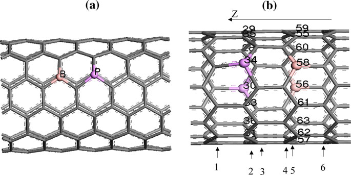
larger than that of C atom and another one is that there is more sp3 hybridization in C-P chemical bonding. The bond angles of C-P-C are in the range 99~103° and bond lengths are in the range 1.705 ~1.798Å. The can be used to illustrate the stability of B-PSWNTs under electric field, which is defined as follows:
| (1) |
where is the total energy of B-PSWNT under different electric field and is the total energy of B-PSWNT without field. Table I lists the difference between total energy of B-PSWNT without electric field and that under different electric fields. It can be seen that the difference of total energies becomes bigger as the electric field increase. These results suggest that that B-PSWNT may get more stable under an extra electric field.
| Type | ( Ha ) |
|---|---|
| B-PSWNT (-0.5V/ Å) | -0.11 |
| B-PSWNT (-1V/ Å) | -0.37 |
| B-PSWNT (0.50V/ Å) | -0.05 |
| B-PSWNT(1V/ Å) | -0.24 |
3.2 energy band structure, density of states and bonding form
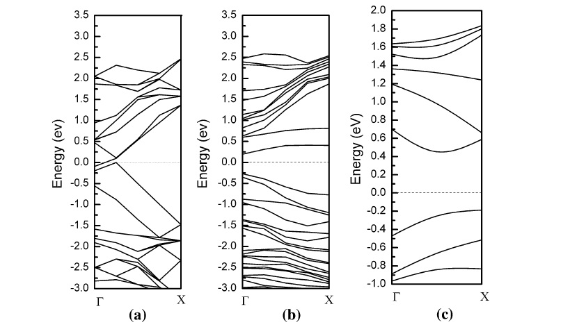
Fig. 2 shows the band structure of intrinsic SWNTs and B-PSWNTs, where (a) and (b) are band structure of the intrinsic and doped (9, 0) type SWNTs. A gap about 0.4626 eV appears in Fig. 2 (b). However, Fig. 2 (a) shows that there is no energy gap in intrinsic (9, 0) type SWNT but an energy level crosses the Fermi energy level. The band structure of another metallic (6, 6) type SWNTs, just as Fig. 2 (c) shows, is also calculated in order to illustrate the common phenomenon that the metallic SWNTs will be converted to semiconductor resulted from the presence of B and P atoms.There is also a band gap about 0.6 eV in the band structure of (6, 6) type B-PSWNTs. Therefore, it is concluded that the metallic SWNT is converted to semiconductor after B/P co-doping, which agrees well with the results of Zhi Xu, Wengang Lu [17]. As far as we know, there is no exact theory to account for such a characteristic. However, we think the main reasons are that the presence of impurities destroys the symmetry of geometry structure, which is viewed as Jahn-Teller effects [24], [25], [26], [27], [28] and that the chemical bonding becomes stronger because of sp3 hybridization.
According to some theories [29], [30](Satio et al 2003; Datta 2005), the (9, 0) type SWNT has D9d symmetry which causes a degeneracy of the energy bands at the boundary of the Brillouin zone. The energy levels of SWNTs are symmetrically disposed about E=0 which locate at the six corners of the Brillouin zone. That is to say that Fermi energy is located at . The requirement of periodic boundary conditions for SWNTs is expressed as follows:
| (2) |
where is the circumferential vector, which defines a series of parallel lines, each corresponding to a different integer value line, giving rise to a set of dispersion relations , one for each subband . The existence of gap depends on whether there exist subbands passing though the corners of the Brillouin zone or not. There exist such subbands for metallic SWNTs, but no such subbands for semiconductors. Therefore, when B atoms and P atoms are injected into the structure of (9, 0) type SWNT, the symmetry of SWNT will be broken. So the symmetry of Brillouin zone also is broken. Therefore, there may be no subbands passing through the corners of the Brillouin zone and a gap arises as Fig. 2 (b) and (c) show. There is always an energy gap at the Fermi energy level in one dimension case whenever the symmetry is broken, which can be concluded from the Jahn-Teller effects.
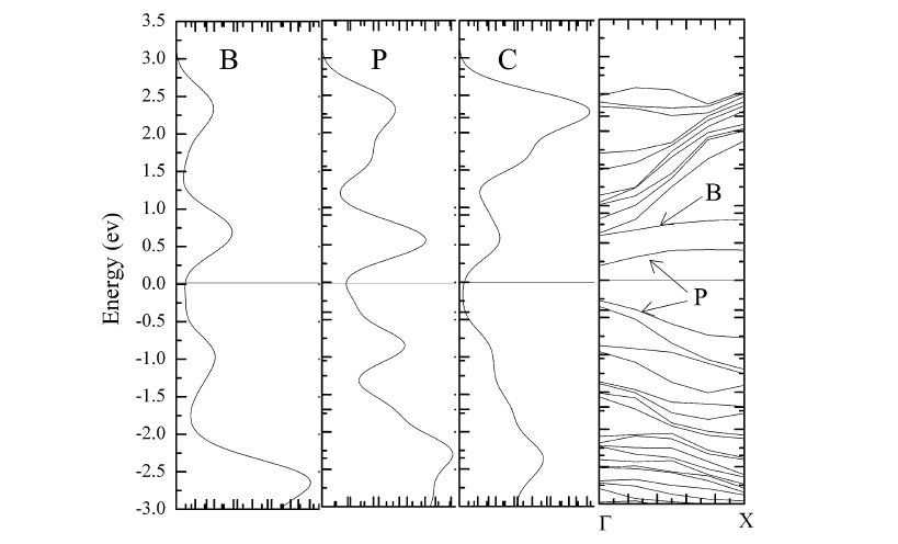
In order to understand the complex electronic structure of B-PSWNTs, the PDOS of (9, 0) B-PSWNT are calculated just as been shown in Fig. 3. There are two impurity levels due to the presence of P atoms at ~ 0.4 eV and ~ -0.75 eV and another impurity level due to the presence of B atoms at ~ 0.7 eV, respectively, by comparing the PDOS of P and B atoms with the energy band structure in Fig. 3. That is quite different from the B/N doped SWNTs. The reason for P impurity level dispersion was explained in our previous study [12]. Fig. 3 also shows that the values of DOS of C atoms are zero near Fermi energy level from the LDOS of C atoms. It suggests that there are no energy levels of C atoms near the Fermi energy level but energy gap comes out. Another reason considered is that the B/P doped SWNT form a hetero-junction because of electrons diffusion owing to the difference from electrons concentrations, which leads to depletion region. It makes the energy gap get wider.
Mulliken population and Mayer bond order [31], [32] were calculated to understand the bonding form. The result data are listed in Tab II. The form Am is used to indicate the atoms, where subscript m is the ordinal of atoms. The Mayer total valences of atoms from the second layer to the fifth layer are listed in the Table II. The second to fifth layer is corresponding to 2st~5th layer of the structure (see Fig. 1), respectively.
Both the valences of P30 and of P34 are 3.2, while the valence of B56 is 3.1 as the same as that of B58. The total valence indicates how many single bonds are associated with the atom [32]. Therefore, both P atom and B atom form about 3 bonds. The values of bond orders of P atoms forming bonding with three C atoms are 0.99, 0.99 and 0.90, while those of B atoms forming bonding with three C atoms are 1.03, 1.04 and 0.94. Being different with above cases, those of C atoms forming bonding each other are in the range 1.11~1.35. The sp3 hybridization mainly forms a single bond. Therefore, there is more sp3 hybridization in P atom than that in B atoms, which is the same as that in C atoms. Therefore, it can be concluded that there is more sp3 hybridization in B/P doped SWNT than that in intrinsic SWNT, which may be another important cause of presence of an energy gap. The Mayer total valence of each C atom in the 2nd, 3rd, 4th and 5th layer is closed to four indicating each C atom with four bonds.
| No.2 layer Mayer | No.3 layer Mayer | No.4 layer Mayer | No.5 layer Mayer |
|---|---|---|---|
| total valence | total valence | total valence | total valence |
| C 28 3.5 | C 1 3.6 | C 46 3.6 | C 55 3.5 |
| C 29 3.5 | C 2 3.7 | C 47 3.6 | B 56 3.1 |
| P 30 3.2 | C 3 3.7 | C 48 3.7 | C 57 3.5 |
| C 31 3.5 | C 4 3.7 | C 49 3.6 | B 58 3.1 |
| C 32 3.5 | C 5 3.6 | C 50 3.6 | C 59 3.6 |
| C 33 3.5 | C 6 3.6 | C 51 3.6 | C 60 3.5 |
| P 34 3.2 | C 7 3.6 | C 52 3.6 | C 61 3.6 |
| C 35 3.5 | C 8 3.7 | C 53 3.7 | C 62 3.6 |
| C 36 3.5 | C 9 3.6 | C 54 3.6 | C 63 3.6 |
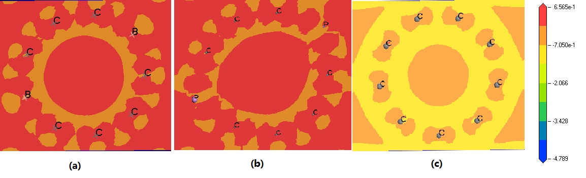
The deformation density is calculated to analyze the bonding forms further. Fig. 4 shows the deformation density of intrinsic (9, 0) type SWNT and that of B/P doped SWNT. Deformation density of the layers B and P atoms locate at are Fig. 4 (a) and (b), respectively. Fig. 4 (c) displays the deformation density of the layer which C atoms locate at in intrinsic SWNT. It is observed that the deformation density is homogeneous in Fig. 4 (c). However, the deformation density is homogeneous inside of annulus but not well-proportioned outside for B-PSWNTs as been shown in Fig. 4 (a). There are fewer electrons in the red area called bonding area, which gets wider after boron and phosphorous are injected. It indicates that there is more sp3 hybridization in that area. It also can be seen that the deformation density is not homogeneous inside and outside of the annulus in Fig. 4 (b). It suggests that there is more sp3 hybridization in the bonding formed by P atoms and C atoms than that formed by B atom and C atom, which agrees well with the analysis of Mayer bond order. The bonds of B-PSWNT become stronger in comparison to the similar bonds of intrinsic SWNT. According to the distribution of deformation density in Fig. 4 (a) and (b), there are lots of delocalized orbitals. Therefore, the electron transfer will happen in B/P doped SWNT. The space charge region is produced when the electron transfer happens.
4 Quantum conductance
Quantum conductance is calculated to study the quantum transport of this hetero-junction. Carbon nanotubes are the quasi one dimensional nano-wire. The electrons are transported in the form of ballistic transports when the length of nano-wire is shorter than the mean free path of an electron under low temperature. Ballistic transport consists of single electron conduction with no phase and momentum relaxation. When chemical dopants are introduced into the C lattice, the impurity-induced backscattering becomes severely strong [33], yielding a very small mean free path so that electrons are strongly backscattered on the impurity level. However, quasiballistic behavior is restored under the proper condition according to work R. Avriller’s work [34] which mainly studied the effect of tube length and the magnetic field on the quantum conductance of CNTs. Doping by physisorption or chemical substitutions made great impact on the quantum transport of CNTs. Ch. Adessi’s study [35] which demonstrated that doping by physisorption will decrease charge-carrier mobilities much less than chemical substitution introducing strong backscattering at the resonance energies of the“quasibound” states associated with the defect potential well. Three type transport regimes including quasi-ballistic, intermediate and localized regime have been studied by R. Avriller et al [36]. The case of (9, 0) considered in this study is quite different from the case R. Avriller group studied. Comparing R. Avriller’s work in which characteristic transport length scales like the elastic mean free path and the localization length were studied, the length of this tube is about 7.032 Å which is great shorter than the mean free path or the elastic mean free path (about 17.8 nm in this case). Therefore, our study focus on the ballistic transport of B-P doped SWNTs. The feature of quantum transport of the p-n junction region is main study in this section. The quantum conductance can be attained by Landauer formula [30], [37] which demonstrates that quantum conductance is determined by the number of the energy level across the Fermi energy level. The Landauer formula is written as follows:
| (3) |
| (4) |
where is the number of energy level across the Fermi energy level. Since the number of sub-energy band equal to the integral value of the density of states, the distribution of under various electric fields as a function of energy range can be described as Fig. 5.
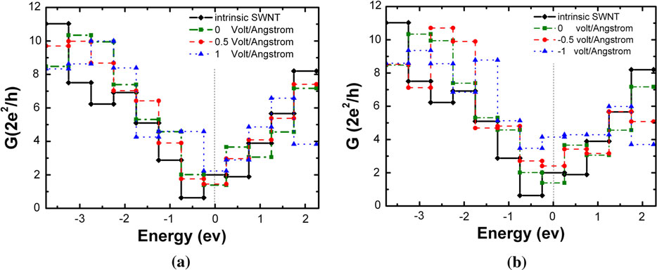
A uniform extra electric field is applied along the direction of the tubes and the positive direction is defined as Z direction (see Fig. 1) to calculate the characteristic of electron transport. The range of electric field strength varies from -1.0 to1.0 V/Å. The quantum conductance is shown in Fig. 5. We define that the electric field is positive along the Z direction (see Fig. 1). Therefore, Fig. 5 (a) and (b) show the quantum conductance of (9, 0) case under the positive and negative electric field, respectively. Fig. 5 (a) shows that the quantum conductance of intrinsic (9, 0) type SWNT is 2 and that of B/P doped SWNT is about 1.3 when electric field strength is 0V/Å. Substitutional doping in CNTs will induce backscattering efficiency which reduced charge mobility and will strongly impact on the on-current capability of CNTs [35]. But the main reason for the decrease of the conductance is effects of the build-in field formed by B/P co-doping. The blow phenomenon can well interpret such reason. When electric field strength increases up to 0.5V/Å, there are not few changes of . As electric field increases to 1V/Å, the quantum conductance is up to 2. Therefore, figure 5 (a) suggests that the hetero-junction of B/P SWNTs may be broken down under the electric field with 1 V/Å according to varied value of quantum conductance as a function of electrical field. This can be explained by the Tunneling Effect because the junction described in Fig. 6 becomes narrow under the electric field with 1 V/Å. Just as Fig. 5 (b) described, when the electric field strength is -0.5 V/Å, the quantum conductance is closed to 3. What’s more, the quantum conductance will increase to 5 under the electric field with -1 V/Å. The potential barrier weakens as the electrical field is increased positively so that the quantum conductance increases. While the electrical field becomes negative the carries can be transported under the electrical field. It is therefore concluded that the B/P doped SWNT behaves like p-n junction.
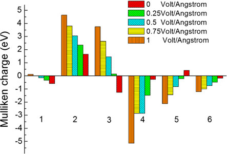
The electronic distribution in the B-PSWNTs is determined by Mulliken charge population as the Fig. 6 shows. The electronegative of C atom is larger than that of B atom resulting in the fact that the fifth layer B atoms locate in are positive and that the nearest neighbor layers are in reverse. However, the second layer P atoms locate in is positive because P atoms give electronics to the C atoms to take part in sp3 hybridization, which is quiet different from the fifth layer. It can be seem that the p-n junction main locates between the second and the third layer without applying extra electric field while the position of p-n junction shift to the interface between the third and the fourth layer gradually as electric field increase. Therefore, the p-n junction has the tendency to be formed in the layers between the layers in which P and B atoms locate. It is important to note that the length of p-n junction get longer when the electric field is 0.25 V/ Å. Since the charge of the second layer is nearly zero, which may leads to decrease of the conduction. But the length will become shorter with the electric field increase resulting in the increase of conduction. The above results agree well with what the Fig. 5 demonstrates.
5 CONCLUSION
By calculating the characteristics of B-P doped (9, 0) and (6, 6) type SWNT using the first principle based on DFT, it concludes that the metallic SWNT will convert to semiconductor because of the B/P co-doping. The main reasons are that the symmetry is broken and that there are more sp3 hybridizations in B/P doped SWNT than those in intrinsic SWNT. It is also seen that the band structure of B-PSWNTs is special owing to the special band structure of P doped SWNTs. Lastly, Mulliken charge population and the quantum conductance of that hetero-junction are calculated to study the electrons transport. The study of quantum conductance suggests that this hetero-junction has the characteristics of p-n junction. Finally, it found that the position of p-n junction of B-PSWNTs will be changed under the electric field by the Mulliken charge population analysis, which will be significance for SWNTs application in nano-device in the future.
References
- [1] S. Iijima et al. Helical microtubules of graphitic carbon. nature, 354(6348):56–58, 1991.
- [2] M. Jose-Yacaman, M. Miki-Yoshida, L. Rendon, and J. G Santiesteban. Catalytic growth of carbon microtubules with fullerene structure. Applied physics letters, 62(2):202–204, 1993.
- [3] M. S Dresselhaus, G. Dresselhaus, and R. Saito. Physics of carbon nanotubes. Carbon, 33(7):883–891, 1995.
- [4] J. C Charlier, X. Blase, and S. Roche. Electronic and transport properties of nanotubes. Reviews of modern physics, 79(2):677, 2007.
- [5] S. J Tans, A. R. M Verschueren, and C. Dekker. Room-temperature transistor based on a single carbon nanotube. Nature, 393(6680):49–52, 1998.
- [6] R. S Lee, H. J Kim, J. E Fischer, A. Thess, and R. E Smalley. Conductivity enhancement in single-walled carbon nanotube bundles doped with k and br. Nature, 388(6639):255–256, 1997.
- [7] Q. L Williams, X. Liu, W. Walters Jr, J. G Zhou, T. Y Edwards, F. L Smith, G. E Williams, and B. L Mosley. Boron-doped carbon nanotube coating for transparent, conducting, flexible photonic devices. Applied Physics Letters, 91:143116, 2007.
- [8] S. H. Lim, R. Li, W. Ji, and J. Lin. Effects of nitrogenation on single-walled carbon nanotubes within density functional theory. Physical Review B, 76(19):195406, 2007.
- [9] S. Ishii, T. Watanabe, S. Ueda, S. Tsuda, T. Yamaguchi, and Y. Takano. Resistivity reduction of boron-doped multiwalled carbon nanotubes synthesized from a methanol solution containing boric acid. Applied Physics Letters, 92(20):202116–202116, 2008.
- [10] Y. S Min, E. J Bae, U. J Kim, E. H Lee, N. Park, C. S Hwang, and W. Park. Unusual transport characteristics of nitrogen-doped single-walled carbon nanotubes. Applied Physics Letters, 93:043113, 2008.
- [11] I. O Maciel, J. Campos-Delgado, E. Cruz-Silva, M. A Pimenta, B. G Sumpter, V. Meunier, F. Lopez-Urias, E. Munoz-Sandoval, H. Terrones, M. Terrones, et al. Synthesis, electronic structure, and raman scattering of phosphorus-doped single-wall carbon nanotubes. Nano letters, 9(6):2267–2272, 2009.
- [12] A. Q Chen, Q. Y Shao, and Z. C Lin. Effects of phosphorus-doping upon the electronic structures of single wall carbon nanotubes. Science in China Series G: Physics Mechanics and Astronomy, 52(8):1139–1145, 2009.
- [13] P. Ayala, M. H R\textbackslashÃŒmmeli, T. Gemming, E. Kauppinen, H. Kuzmany, and T. Pichler. CVD growth of single-walled b-doped carbon nanotubes. physica status solidi (b), 245(10):1935–1938, 2008.
- [14] A. Caillard, C. Charles, R. W Boswell, and P. Brault. Synthesis of carbon nanofibers and pt-nanocluster-based electrochemical microsystems by combining low-pressure helicon plasma techniques. Plasma Science, IEEE Transactions on, 36(4):882–883, 2008.
- [15] E. Cruz-Silva, D. A Cullen, L. Gu, and J. M Romo-Herrera. Heterodoped nanotubes: Theory, synthesis, and characterization of phosphorus- nitrogen doped multiwalled carbon nanotubes. ACS nano, 2(3):441–448, 2008.
- [16] Y. J Kang, Y. H Kim, and K. J Chang. Electrical transport properties of nanoscale devices based on carbon nanotubes. Current Applied Physics, 9(1):S7–S11, 2009.
- [17] Z. Xu, W. Lu, W. Wang, C. Gu, K. Liu, X. Bai, E. Wang, and H. Dai. Converting metallic Single-Walled carbon nanotubes into semiconductors by Boron/Nitrogen Co-Doping. Advanced Materials, 20(19):3615–3619, 2008.
- [18] W. L. Wang, X. D. Bai, and E. G. Wang. Towards the single-walled b-and/or n-doped carbon nanotubes. International Journal of Nanoscience, 6(6):431–442, 2007.
- [19] W. L Wang, X. D Bai, K. H Liu, Z. Xu, D. Golberg, Y. Bando, and E. G Wang. Direct synthesis of BCN single-walled nanotubes by bias-assisted hot filament chemical vapor deposition. Journal of the American Chemical Society, 128(20):6530–6531, 2006.
- [20] B. Delley. An all-electron numerical method for solving the local density functional for polyatomic molecules. The Journal of chemical physics, 92:508, 1990.
- [21] B. Delley. From molecules to solids with the DMol approach. The Journal of Chemical Physics, 113:7756, 2000.
- [22] J. P Perdew, K. Burke, and M. Ernzerhof. Generalized gradient approximation made simple. Physical Review Letters, 77(18):3865–3868, 1996.
- [23] J. P Perdew and Y. Wang. Accurate and simple analytic representation of the electron-gas correlation energy. Physical Review B, 45(23):13244, 1992.
- [24] H. A Jahn and E. Teller. Stability of polyatomic molecules in degenerate electronic states. i. orbital degeneracy. Proceedings of the Royal Society of London. Series A, Mathematical and Physical Sciences, 161(905):220–235, 1937.
- [25] R. Janes and E. A Moore. Metal-ligand bonding. Open University Press, 2004.
- [26] F. G Klärner. About the antiaromaticity of planar cyclooctatetraene. Angewandte Chemie International Edition, 40(21):3977–3981, 2001.
- [27] C. D Stevenson and Y. S Kim. Observation of both Jahn-Teller distorted forms (b1g and b2g) of the cyclooctatetraene anion radical in a 1, 2-Disubstituted system. Journal of the American Chemical Society, 122(13):3211–3215, 2000.
- [28] M. J Bearpark, L. Blancafort, and M. A Robb. The pseudo-Jahn-Teller effect: a CASSCF diagnostic. Molecular Physics, 100(11):1735–1739, 2002.
- [29] R. Saito, G. Dresselhaus, M. S Dresselhaus, et al. Physical properties of carbon nanotubes, volume 3. Imperial College Press London, 2003.
- [30] S. Datta. Quantum transport: atom to transistor. Cambridge Univ Pr, 2005.
- [31] R. S Mulliken. Electronic population analysis on LCAO [Single bond] MO molecular wave functions. II. overlap populations, bond orders, and covalent bond energies. The Journal of Chemical Physics, 23:1841, 1955.
- [32] I. Mayer. Bond orders and valences from ab initio wave functions. International Journal of Quantum Chemistry, 29(3):477–483, 1986.
- [33] B. Biel, X. Blase, F. Triozon, and S. Roche. Anomalous doping effects on charge transport in graphene nanoribbons. Physical review letters, 102(9):96803, 2009.
- [34] R. Avriller, S. Latil, F. Triozon, X. Blase, and S. Roche. Chemical disorder strength in carbon nanotubes: Magnetic tuning of quantum transport regimes. Physical Review B, 74(12):121406, 2006.
- [35] C. Adessi, S. Roche, and X. Blase. Reduced backscattering in potassium-doped nanotubes: Ab initio and semiempirical simulations. Physical Review B, 73(12):125414, 2006.
- [36] R. Avriller, S. Roche, F. Triozon, X. Blase, and S. Latil. Low-dimensional quantum transport properties of chemically-disordered carbon nanotubes: from weak to strong localization regimes. Modern Physics Letters B, 21(29):1955–1982, 2007.
- [37] B. J Van Wees, H. Van Houten, C. W. J Beenakker, J. G Williamson, L. P Kouwenhoven, D. Van der Marel, and C. T Foxon. Quantized conductance of point contacts in a two-dimensional electron gas. Physical Review Letters, 60(9):848–850, 1988.