Electrochemical ferroelectric switching: The origin of polarization reversal in ultrathin films
Abstract
Against expectations, robust switchable ferroelectricity has been recently observed in ultrathin (1 nm) ferroelectric films exposed to air [V. Garcia , Nature (London) 460, 81 (2009)]. Based on first-principles calculations, we show that the system does not polarize unless charged defects or adsorbates form at the surface. We propose electrochemical processes as the most likely origin of this charge. The ferroelectric polarization of the film adapts to the external ionic charge generated on its surface by redox processes when poling the film. This, in turn, alters the band alignment at the bottom electrode interface, explaining the observed tunneling electroresistance. Our conclusions are supported by energetics calculated for varied electrochemical scenarios.
I Introduction
Complex oxides have long been viewed as possible candidates for the next generation of electronic devices, which require reduced feature sizes, enhanced operating speeds and low consumption. Amongst oxides, ferroelectrics offer the ability to store information in a non-volatile manner via fast reversible polarization switching in ferroelectric random-access memory (FeRAM). The observation of giant tunneling electroresistance (TER) Garcia et al. (2009) in ultrathin (3 unit cells) ferroelectric films has recently opened a novel paradigm for device design based on these materials Zubko and Triscone (2009); Segal (2009).
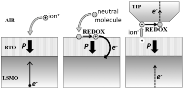
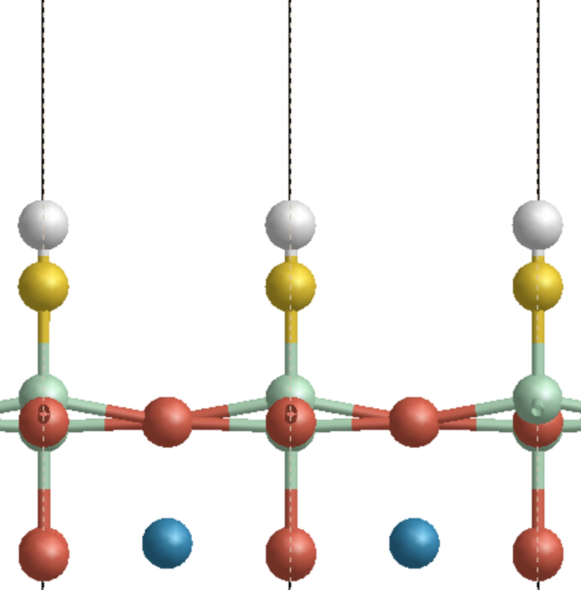
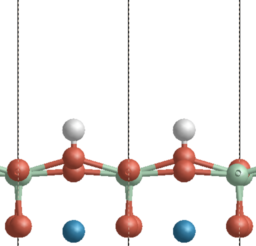
Although the experiments Garcia et al. (2009) ascribed TER to ferroelectricity, which appeared robust and switchable, how the polar state is stabilized in such thin films is by no means established. In principle, a ferroelectric film with an exposed surface cannot sustain a monodomain polarization perpendicular to the surface, because of the strong depolarizing field that would inevitably arise 111 The polarization is clearly observed to be perpendicular to the interface, consistent with the expected behavior of compressively strained films Schlom et al. (2007). . Charged particles from the environment could in principle cancel the depolarizing field Fridkin (1980) (Fig. 1 left). So far, however, the only chemical control of switching in air relates to neutral species, O2 Wang et al. (2009); Fong et al. (2006); Spanier et al. (2006) (Fig. 1 center). It is then not clear how neutral gas-phase molecules could interact with a biased atomic force microscopy (AFM) tip to produce the polar state.
Here we argue that the voltage applied with the AFM tip induces electrochemical switching (Fig. 1 right), i.e. redox processes that are essential to liberate free charge and therefore screen the depolarizing field. This process would act as a nanobattery, rather than a nanocapacitor. Note that the same mechanism could explain other effects at oxide interfaces, such as the switchable two-dimensional electron gas (2DEG) at the LaAlO3/SrTiO3 interface Cen et al. (2008); Bristowe et al. (2011), where the switching appears to be mediated by surface charge Xie et al. (2010).
To explore this mechanism we consider the system studied experimentally in Ref. Garcia et al., 2009, consisting of a compressively strained nanometer-thick BaTiO3 (BTO) film on a La0.7Sr0.3MnO3 (LSMO) bottom electrode. Here we show, using first principles calculations, that (i) the pristine system (clean BTO surface with an ideal TiO2 termination) does not allow for a ferroelectric polarization, , normal to the surface despite the large compressive strain; (ii) a non-zero is crucially dependent on the presence of a surface external ionic charge, in the form of defects or adsorbates; and (iii) the energetics for the formation of oxidized or reduced surface defects support the electrochemical switching model. We also find (iv) a systematic change in band offset with screening charge density, which we identify as the microscopic mechanism behind the experimentally observed TER Garcia et al. (2009), and (v) a large magnetoelectric coupling, due to the accumulation or depletion of spin-polarized carriers at the interface with ferromagnetic LSMO. The connection between these effects can be summarized as follows: under open-circuit boundary conditions the electric displacement field within the film, the change in magnetization at the interface and the interface dipole, are all proportional (or equal) to the external ionic charge density, per unit surface , produced by the redox processes.
II Methods
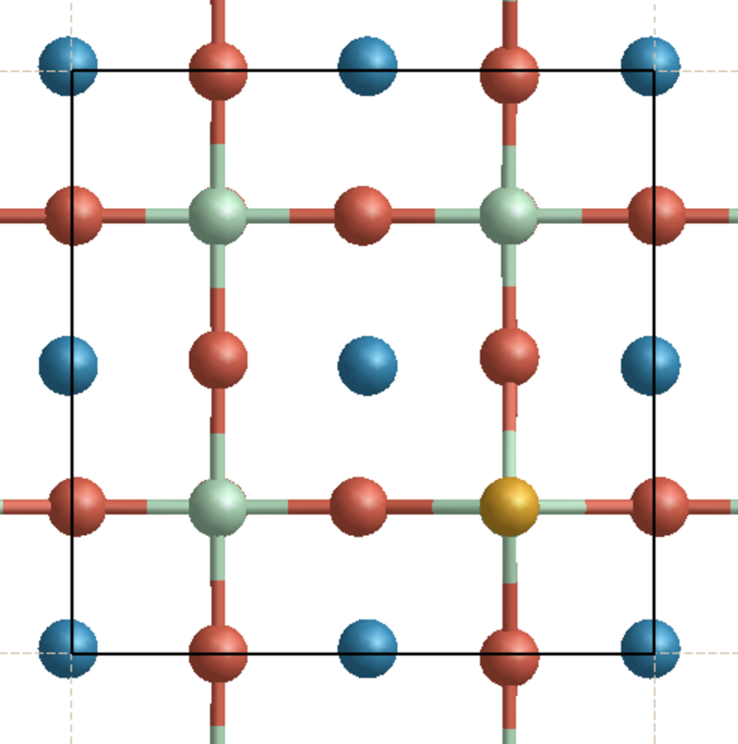
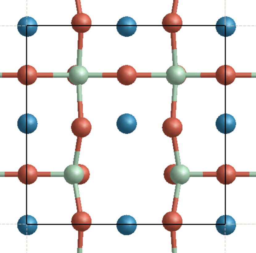
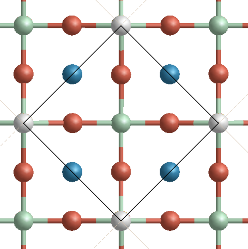
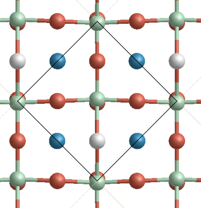
The density-functional theory (DFT) calculations are performed using the spin-polarized Wu-Cohen (WC) exchange-correlation functional Wu and Cohen (2006), as implemented in the Siesta code Ordejon et al. (1996); Soler et al. (2002) 222 Details of the pseudopotentials, numerical atomic orbitals and LSMO doping are given in Ref. Ferrari et al., 2006 and Junquera et al., 2003.. We find GGA-WC to reproduce bulk Ferrari et al. (2006) and surface Ferrari et al. (2006); Pruneda et al. (2007) properties of LSMO that were calculated using the Perdew-Burke-Ernzerhof (PBE) scheme Perdew et al. (1996); at the same time, GGA-WC is more appropriate for ferroelectric oxides. The LSMO/BTO system consists of 5.5 unit cells of LSMO (MnO2-terminated) stacked with 3 unit cells of BTO along the direction in a slab geometry. The supercell contains a 15 Å thick vacuum layer and has either 22 or in-plane periodicity (see Fig. 2). The 5.5 unit cells of LSMO are thick enough to show bulk-like features in the center, and 3 unit cells of BTO was experimentally shown to be thick enough for ferroelectricity Garcia et al. (2009). We use a dipole correction to simulate open-circuit boundary conditions, enforcing zero macroscopic electric field in the vacuum layer. We constrain the in-plane lattice parameter to experimental bulk NdGaO3 (NGO) to reproduce the experimental conditions of Ref. Garcia et al. (2009); this imposes a large (3%) compressive strain on BTO. Based on this slab geometry, we perform a number of calculations where we vary the surface composition by introducing defects or adsorbates. In particular, we simulate the clean TiO2-terminated surface (we shall refer to this structure as “pristine” henceforth); one O vacancy (“O-vac”) or adatom (“O-ads”) per 22 surface cell; one H adatom (“H”) or OH group (“OH”) per cell 333Atomic forces were relaxed to less than 40 meV/Å.. Hereafter we shall discuss the results with special regard for the presence or absence of ferroelectric polarization in each case.
III Discussion
III.1 The pristine system
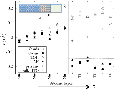
Fig. 2 shows the relaxed out-of-plane structural distortions as a function of the surface chemical environment. The pristine system is characterized by negligible distortions in the interior of the BTO film, suggesting the absence of macroscopic in this system. Only a surface rumpling is present, resulting in a small net inwards dipole (non-switchable) that decays rapidly towards the bulk (a surface rumpling is a known general feature of oxide surfaces, in particular the TiO2 termination of BTO Padilla and Vanderbilt (1997); Heifets et al. (1997)). A vanishing is consistent with the open-circuit boundary conditions, despite the large compressive strain. In absence of a top electrode the macroscopic electric displacement field in BTO is equal and opposite to the density of external surface charge. As this charge is zero at the clean TiO2 surface, the film is constrained to a paraelectric state.
III.2 Chemical switching
To illustrate possible screening scenarios, we now include representative surface defects 444 Sampling the entire phase space (redox species and density, temperature, partial pressure, polarization) is beyond the scope of this work, but can be done within thermodynamic theory (see Ref. Stephenson and Highland, 2011).. The O-vac and O-ads systems are both characterized by large ferroelectric distortions (Fig. 2). These are comparable to the strained bulk, where we calculate a spontaneous polarization =0.369 C/m2 (0.35 ). This result is again consistent with the constraint that . In fact, one oxygen defect for every 22 unit cells (0.5 ) yields a larger surface charge than what would be sufficient to screen . This justifies the larger cation-anion rumplings that we obtain in the film compared with the bulk (Fig. 2). OH and H adatoms (with coverage to maintain ) produce distortions of similar magnitude (Fig. 2). This confirms the generality of the ferroelectric switching mechanism: the ferroelectric state really depends on the net surface charge, and not on the chemical identity of the adsorbed species.
In order to study the electrochemical switching (Fig. 1 right), we commence by analyzing switching (Fig. 1 center). Both are controlled by redox processes that transform bound charge into free charge, allowing for an electronic transfer between the surface defect and the metal substrate, but have different associated chemical sources/drains and energetics. Chemical switching was recently shown in a system consisting of PbTiO3 on SrRuO3 Fong et al. (2006); Wang et al. (2009) and BTO films on Au or vacuum Spanier et al. (2006).
To assess whether these redox reactions are thermodynamically accessible in typical experimental conditions, we estimate the formation energy of the defective systems taking the reactions: 1) Slab(pristine) Slab(O-vac)+1/2O2 and equivalent for O-ads, 2) 1/2H2O+1/4O2+Slab(pristine) Slab(OH) and 3) 1/2H2O+Slab(pristine) Slab(H)+1/4O2. The chemical potential of the relevant molecular species is set to the calculated total energy of the spin-polarized molecule in a large cubic box. The results are summarized in Table 1. They suggests that, whilst the oxygen adatom is likely to form under oxygen-rich conditions, the formation energy for the oxygen vacancy is possibly too high to form even in oxygen-poor conditions. The calculated OH and H formation energies suggest that water is a very likely redox intermediate. Note that H2O is ubiquitous in most experiments performed in air, and was recently found to play a crucial role in AFM experiments performed on LaAlO3/SrTiO3 Bi et al. (2010). Since both sets of reactions involve oxygen, we therefore expect that altering the surrounding oxygen partial pressure would affect the stability of reduction or oxidation processes, consistent with the recently observed chemical switching Wang et al. (2009).
| O-vac | O-ads | OH | H | |
| (eV) | +3.6 | -0.4 | -1.5 | +0.9 |
III.3 Electrochemical switching
Now we discuss how the electrochemical processes could proceed in practice during the AFM switching experiments of Ref. Garcia et al., 2009 (general electrochemical processes on oxide surfaces are reviewed in Ref. Kalinin et al., 2011; Waser et al., 2009). As schematically shown in Fig. 1 (right), a biased tip close to contact can remove surface ions. These would then undergo a redox reaction at the tip surface. This process is favored by the energy associated with the biased external circuit, , but costs an energy equal to the change in binding energy of the ion to the ferroelectric surface and to the tip surface, (this effectively redefines the relevant chemical potential). By minimizing the Gibbs free energy of the system (see e.g. Ref. Stephenson and Highland, 2011 or Morozovska et al., 2010) it can be shown that poling can stabilize redox defects if , after which the equilibrium redox charge density, , and polarization both grow with . This electrochemical process would then act as a nanobattery, rather than a nanocapacitor. By controlling the environment (species and chemical potential) and , one may be also able to selectively control the active redox reaction, potentially opening new routes to surface redox catalysis. After removal of the tip, the surface redox density from poling can remain, since the reverse reaction is now blocked by key reactants being removed with the tip. This would explain the observation of Ref. Garcia et al., 2009 that the domains are stable for a very long time after “writing”. Of course, lateral charge diffusion across domain boundaries Kalinin and Bonnell (2004) may still occur in principle, but kinetic barriers are likely to hinder such processes. Therefore the bulk polarization, , is expected to be an estimate of the equilibrium polarization after poling. We note that unlike in the LaAlO3/SrTiO3 system where the polarization is driving the surface chemistry Bristowe et al. (2011), in ferroelectric films we expect it is the surface chemistry (and poling) that is driving the polarization. This is because the energy scale for changing the polarization is much larger in LaAlO3 than in the ferroelectric.
III.4 Magnetoelectric coupling
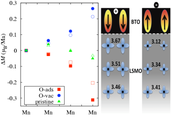
The electronic transfer mechanism can be quantitively estimated through the change in magnetization of LSMO. LSMO is a half-metal with only Mn 3 majority spin levels around the Fermi level. As the screening carriers are fully spin-polarized, an electronic transfer between LMSO and the BTO surface results in a systematic change of the magnetization near the interface. We calculate the change in magnetization from the pristine to the O-vac and O-ads systems and to the 2OH and 2H systems, , as 1.7 and 1.5 in the supercell, equivalent to 0.42 and 0.37 respectively (the remaining 0.1 electrons/holes stay in BTO, see Appendix). This extra electron density (which corresponds to the electric displacement, , because of the half-metallic nature of LSMO) resides in the interface region, decaying into the electrode with an associated Thomas-Fermi screening length (see Fig. 3). This situation is similar to the carrier-mediated magnetoelectricity already predicted at SrTiO3/SrRuO3 interfaces Rondinelli et al. (2007) and in LSMO/BTO superlattices Burton and Tsymbal (2009). In agreement with Ref. Burton and Tsymbal, 2009 a competing interface antiferromagnetic type phase (called A1 in Table 1 of Ref. Burton and Tsymbal, 2009) was found for the outwards BTO polarization. A similar magnetoelectric effect has recently been experimentally realized Vaz et al. (2010); Molegraaf et al. (2009).
III.5 Tunneling Electroresistance
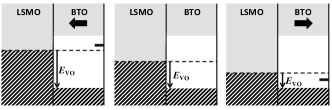
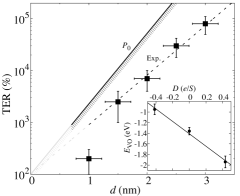
We now discuss how the electrochemical switching process may lead to the giant TER observed in the LSMO/BTO system Garcia et al. (2009). In the simplest semiclassical approximation, TER has an exponential dependence on the tunneling barrier shape Gruverman et al. (2009). The interface dipole, and hence band offset (), at a metal/ferroelectric interface depends linearly on the electric displacement field, , in a way that can be expressed with an effective screening length Junquera and Ghosez (2003); Zhuravlev et al. (2005); Kohlstedt et al. (2005), . For LSMO-BTO we calculate Å. Using the calculated values of the band offset (Fig. 4 inset) and the experimental band gap of BTO, we obtain the change in barrier height upon complete polarization reversal (for the potential in BTO is flat, i.e. the tunneling barrier shape is rectangular), , and the average barrier height, . These values then yield an estimate of the TER using the exponential dependence Gruverman et al. (2009) on the barrier thickness, , for large TER,
| (1) |
Fig. 4 compares this estimate with the experimental data Garcia et al. (2009) showing that this simple model captures remarkably well the essential physics of TER in this system. We note a recent study reported comparable shifts in (measured using photoelectron spectroscopy) on a similar ferroelectric/LSMO system upon polarization reversal Wu et al. (2011). The origin of electroresistance effects in oxide nanotubes has also recently been suggested as redox reactions Nonnenmann et al. (2010). However the redox arguments there are fundamentally different - it is proposed that the electrons yielded by oxygen vacancies are directly available for conduction.
IV Conclusions
In conclusion we have studied an electrochemical mechanism for ferroelectric switching in thin films and proposed it as the origin of switchable ferroelectricity, TER and magnetoelectricity in a prototypical system. This work opens several avenues for future research. From the experimental point of view, it would be interesting to investigate the composition of a ferroelectric surface before and after switching (e.g. via the AFM tip), to verify whether reduced or oxidized gas-phase species are present (as suggested by our results). Also, this point could be indirectly checked by performing the AFM-mediated switching experiments in a controlled atmosphere, in analogy to the experiments of Bi et al. [19] on LAO/STO. From the theoretical point of view, a natural next step would be to perform a more detailed thermodynamic analysis of the stability of a ferroelectric surface (either pristine or decorated with adsorbates). This would involve exploring different coverages, possible inhomogeneous polarization states, and the effect of temperature and other external perturbations. We hope that our results will stimulate further investigations along these (and possibly other) directions.
Acknowledgements.
We acknowledge G Catalan, J Íñiguez, M Bibes, V Garcia, N Mathur, X Moya, J Junquera, C Ocal and S Streiffer for valuable discussions, the support of EPSRC, NANOSELECT and MCINN FIS2009-12721-C04-01 and computing resources of CamGRID at Cambridge, the Spanish Supercomputer Network and HPC Europa. PBL acknowledges DOE support under FWP 70069.


*
Appendix A
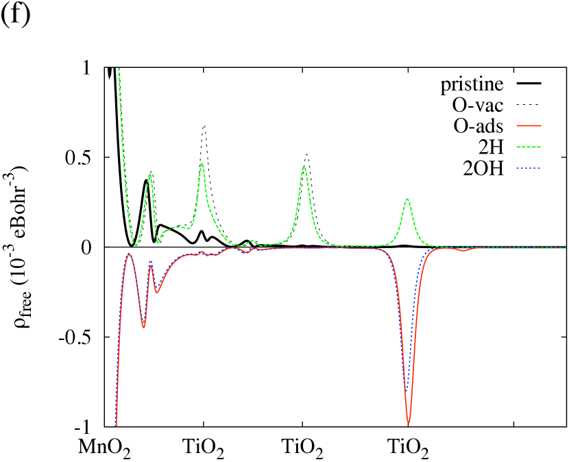
Here we provide details of the electronic structure of the various LSMO/BTO systems. Figure 5 (a)-(e) shows the spin-resolved layer-by-layer density of states for the pristine, O-ads, O-vac, 2OH and 2H systems. As discussed in the main text, the electric displacement and polarization within BTO, and , and hence the valence band offset, , depend only on , the surface defect charge density, and not the surface chemistry. However, as discussed in Ref. Stengel et al., 2011, this is not strictly the case once becomes negative or reaches the band gap of BTO. At this point electrons or holes “spill out” in to the BTO layer. This “charge spill out” regime is favored by DFT, which often underestimates the band gap, and therefore can be an artifact of the calculation.
In our case, due to the presence of a free surface, there is a further issue that was not explicitly considered in Ref. 35, i.e. the effect of surface states. In many cases, these fall within the bulk band gap of the ferroelectric film, and might cross the Fermi level of the metal, thus causing a significant spill-out of charge even when the bulk electronic bands are not directly affected. Note that surface states in ferroelectrics typically have a marked localized orbital character (either the atomic orbital of an adsorbate, or the 3 orbitals of the transition metal cation). Therefore, it is reasonable to suspect that DFT might introduce systematic errors in their ionization energies (similarly to the energy location of the bulk band edges discussed in Ref. 35), and the metallization of a surface state should be regarded with analogous caution (for a detailed discussion of charge transfers at surfaces see, e.g., Ref. Stengel, 2011).
Refs. Stengel et al., 2011 and Stengel, 2011 prescribe an analysis of the hole- and electron-like charge spill out. Following this prescription, we determine the free electron density profile, , within BTO in Fig. 5(f) (using Eq. 25 and 26 of Ref. Stengel et al., 2011 and Eq. 19 of Ref. Stengel, 2011 for hole spill out). Out of all the five systems, the pristine one is unaffected, the negatively polarized (O-vac and 2H) systems are affected by electron spill out into the conduction band, and the two positively polarized (O-ads and 2OH) ones are affected by hole spill out into surface states (see Fig. 5). In both O-vac and 2H amounts to approximately 0.03 electrons per unit cell of BTO , which is a fairly mild effect (compare with approximately 0.15 electrons per unit cell in the KNO/SRO system of Ref. Stengel et al., 2011). In the case of O-ads and 2OH, the surface O(2) states accommodate a total of approximately 0.1 holes per surface perovskite unit (Fig. 5(f)). Of course, estimating to what degree this charge spill is problematic, depends not only on the magnitude but also the purpose of the calculation. The charge spill out induces an error in two quantities that are discussed in this work: the total injected charge into the LSMO electrode, and the band alignment. Considering the total injected charge, the impact of this error is trivial to estimate. In fact, 0.03 electrons per cell times , number of BTO cells, corresponds exactly to the difference between the actual induced spin in LSMO and the “ideal” limit of 2 Bohr magnetons per cell. This observation can be directly used to estimate the error in the calculated band offset. In fact, we can assume in a first approximation that the band offset is linear in the electric displacement of the BTO cell adjacent to the interface, . Using the above numbers for the O-vac system,
| (2) |
where is the induced spin, and is the supercell surface area (or reciprocal of the defect density). This provides an accurate estimate of the actual electric displacement “felt” by LSMO. Using this information, therefore, we can make a very accurate estimation of the linear band offset dependence with . We used this analysis to make the plot shown in Fig. 4 inset of the main text. Therefore, whilst we understand the limitations of DFT, in this case they do not affect significantly our conclusions.
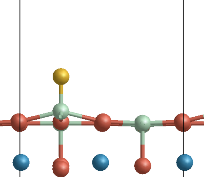
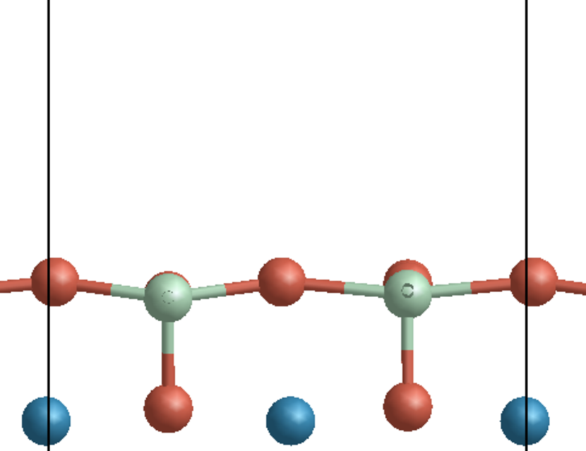
Figure 6 displays the relaxed atomic structures of the BTO surface with O-ads, O-vac, 2OH and 2H.
References
- Garcia et al. (2009) V. Garcia, S. Fusil, K. Bouzehouane, S. Enouz-Vedrenne, N. Mathur, A. Barthélémy, and M. Bibes, Nature 460, 81 (2009).
- Zubko and Triscone (2009) P. Zubko and J. Triscone, Nature 460, 45 (2009).
- Segal (2009) M. Segal, Nature Nanotechnology (2009).
- Fridkin (1980) V. Fridkin, Ferroelectric semiconductors (Consultants Bureau, 1980), ISBN 0306109573.
- Wang et al. (2009) R. Wang, D. Fong, F. Jiang, M. Highland, P. Fuoss, C. Thompson, A. Kolpak, J. Eastman, S. Streiffer, A. Rappe, et al., Phys. Rev. Lett. 102, 47601 (2009).
- Fong et al. (2006) D. Fong, A. Kolpak, J. Eastman, S. Streiffer, P. Fuoss, G. Stephenson, C. Thompson, D. Kim, K. Choi, C. Eom, et al., Phys. Rev. Lett. 96, 127601 (2006).
- Spanier et al. (2006) J. Spanier, A. Kolpak, J. Urban, I. Grinberg, L. Ouyang, W. Yun, A. Rappe, and H. Park, Nano Lett. 6, 735 (2006).
- Cen et al. (2008) C. Cen, S. Thiel, G. Hammerl, C. W. Schneider, K. E. Andersen, C. S. Hellberg, J. Mannhart, and J. Levy, Nat. Mater. 7, 298 (2008).
- Bristowe et al. (2011) N. C. Bristowe, P. B. Littlewood, and E. Artacho, Phys. Rev. B 83, 205405 (2011).
- Xie et al. (2010) Y. Xie, C. Bell, T. Yajima, Y. Hikita, and H. Hwang, Nano Lett. (2010).
- Wu and Cohen (2006) Z. Wu and R. Cohen, Phys. Rev. B 73, 235116 (2006).
- Ordejon et al. (1996) P. Ordejon, E. Artacho, and J. M. Soler, Phys. Rev. B 53, 10441 (1996).
- Soler et al. (2002) J. Soler, E. Artacho, J. Gale, A. Garcia, J. Junquera, P. Ordejon, and D. Sanchez-Portal, J. Phys.: Condens. Matter 14, 2745 (2002).
- Ferrari et al. (2006) V. Ferrari, J. Pruneda, and E. Artacho, Physica Status Solidi (a) 203, 1437 (2006).
- Pruneda et al. (2007) J. Pruneda, V. Ferrari, R. Rurali, P. Littlewood, N. Spaldin, and E. Artacho, Phys. Rev. Lett. 99, 226101 (2007).
- Perdew et al. (1996) J. Perdew, K. Burke, and M. Ernzerhof, Phys. Rev. Lett. 77, 3865 (1996).
- Padilla and Vanderbilt (1997) J. Padilla and D. Vanderbilt, Phys. Rev. B 56, 1625 (1997).
- Heifets et al. (1997) E. Heifets, S. Dorfman, D. Fuks, and E. Kotomin, Thin Solid Films 296, 76 (1997).
- Bi et al. (2010) F. Bi, D. Bogorin, C. Cen, C. Bark, J. Park, C. Eom, and J. Levy, Appl. Phys. Lett. 97, 173110 (2010).
- Kalinin et al. (2011) S. Kalinin, S. Jesse, A. Tselev, A. Baddorf, and N. Balke, ACS nano 5, 5683 (2011).
- Waser et al. (2009) R. Waser, R. Dittmann, G. Staikov, and K. Szot, Advanced Materials 21, 2632 (2009).
- Stephenson and Highland (2011) G. B. Stephenson and M. J. Highland, Phys. Rev. B 84, 064107 (2011).
- Morozovska et al. (2010) A. Morozovska, E. Eliseev, S. Svechnikov, A. Krutov, V. Shur, A. Borisevich, P. Maksymovych, and S. Kalinin, Phys. Rev. B 81, 205308 (2010).
- Kalinin and Bonnell (2004) S. Kalinin and D. Bonnell, Nano Lett. 4, 555 (2004).
- Gruverman et al. (2009) A. Gruverman, D. Wu, H. Lu, Y. Wang, H. Jang, C. Folkman, M. Zhuravlev, D. Felker, M. Rzchowski, C. Eom, et al., Nano Lett. 9, 3539 (2009).
- Rondinelli et al. (2007) J. Rondinelli, M. Stengel, and N. Spaldin, Nature Nanotechnology 3, 46 (2007).
- Burton and Tsymbal (2009) J. D. Burton and E. Y. Tsymbal, Phys. Rev. B 80, 174406 (2009).
- Vaz et al. (2010) C. A. F. Vaz, J. Hoffman, Y. Segal, J. W. Reiner, R. D. Grober, Z. Zhang, C. H. Ahn, and F. J. Walker, Phys. Rev. Lett. 104, 127202 (2010).
- Molegraaf et al. (2009) H. Molegraaf, J. Hoffman, C. Vaz, S. Gariglio, D. van der Marel, C. Ahn, and J. Triscone, Advanced Materials 21, 3470 (2009).
- Junquera and Ghosez (2003) J. Junquera and P. Ghosez, Nature 422, 506 (2003).
- Zhuravlev et al. (2005) M. Zhuravlev, R. Sabirianov, S. Jaswal, and E. Tsymbal, Phys. Rev. Lett. 94, 246802 (2005).
- Kohlstedt et al. (2005) H. Kohlstedt, N. Pertsev, J. Rodríguez Contreras, and R. Waser, Phys. Rev. B 72, 125341 (2005).
- Wu et al. (2011) C.-L. Wu, P.-W. Lee, Y.-C. Chen, L.-Y. Chang, C.-H. Chen, C.-W. Liang, P. Yu, Q. He, R. Ramesh, and Y.-H. Chu, Phys. Rev. B 83, 020103 (2011).
- Nonnenmann et al. (2010) S. Nonnenmann, E. Gallo, and J. Spanier, Appl. Phys. Lett. 97, 102904 (2010).
- Stengel et al. (2011) M. Stengel, P. Aguado-Puente, N. A. Spaldin, and J. Junquera, Phys. Rev. B 83, 235112 (2011).
- Stengel (2011) M. Stengel, Phys. Rev. B 84, 205432 (2011).
- Schlom et al. (2007) D. Schlom, L. Chen, C. Eom, K. Rabe, S. Streiffer, and J. Triscone, Annu. Rev. Mater. Res. 37, 589 (2007).
- Junquera et al. (2003) J. Junquera, M. Zimmer, P. Ordejon, and P. Ghosez, Phys. Rev. B 67 (2003).