Semi-analytical design of antireflection gratings for photonic crystals
Abstract
This article concerns the design of antireflection structures which, placed on a photonic crystal surface, significantly diminish the fraction of energy lost to reflected waves. After a review of the classes of these structures proposed to date, a new method is presented in detail for the design of antireflection gratings operating in a wide range of angles of incidence. The proposed algorithm is illustrated by means of several examples, showing the advantages and limitations.
I Introduction
Photonic-crystal (PC) devices may become vital ingredients of integrated optical circuits. For instance, they open new possibilities and functionalities like negative refraction Notomi (2000); Pendry (2000); Gralak et al. (2000), supercollimation Enoch et al. (2003); Gralak et al. (2006), compact isolators Wang and Fan (2005); Śmigaj et al. (2010), et c. On the other hand, PCs generally present significant reflectivity at their surface while, in many applications, one strives after a perfect energy transfer between the incident plane wave and the propagative PC eigenmode (or, more rarely, several such modes). An important issue is then to eliminate propagative reflected waves. In this paper we propose a semi-analytical algorithm for the design of gratings acting as wide-angle antireflection (AR) structures for two-dimensional PCs.
The article is organized as follows. In the next section we review existing AR structures for homogeneous media and PCs. Subsequently, in section III, the three steps of the new design procedure are presented in detail. This algorithm is then tested on several particular cases: a PC flat lens (section IV), a supercollimating PC (section V), and a non-reciprocal PC mirror (section VI). Finally, in section VII we discuss briefly the influence of AR gratings in the evanescent-wave regime.
II Background
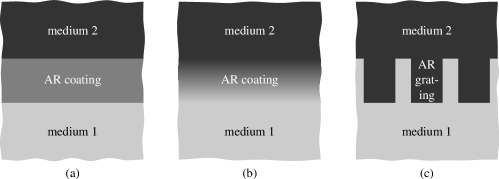
In this section we shall review existing methods of eliminating reflections from interfaces which separate different media. We start with the simpler case of interfaces separating homogeneous media, since the basic tools used to deal with this class of systems turn out to be valuable also when more complex media, such as PCs, are involved. The existing AR solutions can be divided into three broad classes. The refractive index of AR coatings depends only on the coordinate perpendicular to the interface; depending on whether is piecewise-constant or not, we speak of homogeneous-layer or inhomogeneous-layer AR coatings Dobrowolski et al. (2002). In turn, the refractive index of AR gratings is also a function of the coordinates parallel to the interface. Figure 1 shows example AR structures belonging to these three classes.
The simplest homogeneous-layer AR coating consists of a single thin film with refractive index and thickness chosen so as to ensure destructive interference of waves reflected from its top and bottom surfaces, excited by a plane wave with a certain frequency and angle of incidence . The values of and can be obtained analytically. In order to improve the angular and frequency tolerance of the coating, one can increase the number of layers to make the transition between the refractive index of the super- and substrate more gradual Dobrowolski et al. (2002), thus reducing the amplitude of waves reflected on the individual discontinuities of . In the limit of an infinite number of layers, one arrives at an inhomogeneous-layer coating with a continuous monotonic profile . Several specific profiles have been proposed in the literature (see ref. Grann and Moharam, 1996 for a review). Unfortunately, these “ideal” AR coatings, even the single-layer one, cannot usually be realized because of the lack of suitable materials with the required values of . This is the case, in particular, for air-solid interfaces, where thin films with refractive index close to unity are needed.
Short of using special ultra-low-index media, such as so-called Reststrahlen materials Dobrowolski et al. (2002), there are two basic ways of circumventing this problem. One consists in abandoning completely the structures based on a “continuous transition” between the super- and substrate refractive indices in favor of interference-based coatings Dobrowolski et al. (2002). In these systems, the total reflected wave vanishes thanks to the destructive interference of partial waves generated at interfaces between layers with contrasting values of . For instance, so-called -coatings consist of two layers with prescribed refractive indices and (corresponding to realistic materials) and thicknesses and adjusted so as to eliminate reflection at the desired values of and . Note that and must satisfy certain conditions in order that appropriate and can be found (ref. Macleod, 2001, p. 96). A disadvantage of -type AR coatings is that their angular and frequency tolerance are usually inferior even to those of the corresponding ideal single-layer coatings (ref. Macleod, 2001, p. 97; ref. Orfanidis, 2008, p. 188).
The other solution consists in using subwavelength gratings to simulate AR coatings with arbitrary profiles. In many cases, the effective-medium theory of gratings can be employed to calculate the grating profile mimicking the desired dependence Grann and Moharam (1996). Several types of gratings, such as the lamellar, trapezoidal, sinusoidal, triangular and pyramidal ones, have been studied in the literature and shown to have good AR properties Grann and Moharam (1996); Bräuer and Bryngdahl (1994); Raguin and Morris (1993, 1993). A review of the experimental methods used to fabricate such AR structures can be found in ref. Kikuta et al., 2003.
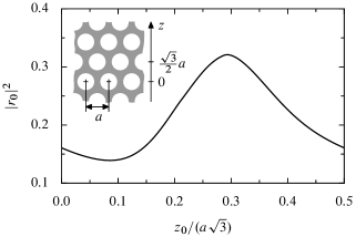
Let us now turn to the case of PCs. One of their distinguishing features is the dependence of their reflection coefficient on the position of their truncation plane. One could hope then that a significant reduction of a PC’s reflectance could be achieved without adding any AR structure, but simply by choosing an appropriate cut. For some crystals, this has indeed proved to be possible Xiao et al. (2004); Botten et al. (2006). In particular, Botten et al. Botten et al. (2006) have shown that very low reflectance is a rather general feature of rod-type PCs truncated midway between successive layers of rods. For many crystals, however, no truncation plane provides a sufficiently small value of reflectance (see fig. 2). This method of reducing reflection is therefore not general enough, and one often has to resort to introducing some AR structure. Several types of them have been proposed in the literature. More often than not, they have much in common with one of the solutions developed with homogeneous materials in mind, reviewed in the previous subsection.
The simplest approach has been proposed by Li et al. Li et al. (2007). It consists in placing in front of the crystal a -type AR coating composed of two layers made of constituent materials of the crystal, usually air and a dielectric. Their thicknesses can be determined analytically or graphically as soon as the reflection coefficient of the semi-infinite uncoated PC at the selected operation frequency is known. This frequency is assumed to be low enough that only the zeroth diffraction order be propagative in the layer closest to the PC surface, so that all higher orders reflected by the crystal decay before reaching the boundary between the two layers. If it is not the case, the structure may still work, but the optimum layer thicknesses will not in general be given by the analytical formulas derived from the thin-film theory. The basic disadvantage of this otherwise very attractive approach is the relatively low angular and frequency tolerance of -type AR coatings.
Another group has studied a similar approach, in which one of the homogeneous layers is replaced by a grating of rods or holes Lee et al. (2008); Park et al. (2009). The performance of the resulting AR gratings was shown to be similar to that of -type coatings Park et al. (2009). Related structures, albeit with only a single degree of freedom (the radius of the outermost rods of a rod-type PC), were also analyzed by Jin and He Jin and He (2007). In turn, Zhang and Li Zhang and Li (2007) proposed a more complex wide-angle AR grating for the interface between air and a PC flat lens, whose fabrication would be seriously hindered, though, by the presence of extremely thin air slits and dielectric veins.
In contrast to the above works, which concentrated on the low-frequency regime, the authors of refs. Baba and Ohsaki, 2001; Baba et al., 2004; Matsumoto et al., 2005 endeavored to eliminate the reflection from an interface between a PC and a semiconductor at a frequency where multiple propagative diffraction orders existed in the latter medium. They proposed an AR grating consisting of elongated drop-shaped air holes, this nonstandard form being motivated by the desire of ensuring a gradual transition between the two media. In fact, the shape of the resulting structure resembles closely the classical trapezoidal AR gratings studied, e.g., by Raguin and Morris Raguin and Morris (1993). The improvement brought about by these gratings has subsequently been demonstrated experimentally Matsumoto et al. (2006). Unfortunately, Baba et al. did not provide any analytical guidelines regarding the choice of the geometrical parameters of the gratings, resorting instead to a time-consuming scan of the parameter space in order to find the optimum structure Baba and Ohsaki (2001); Baba et al. (2004).
A very important contribution was made by Lawrence et al. Lawrence et al. (2008, 2009), who introduced the concept of generalized matrix-valued effective immittance of gratings and showed that their effective-medium description can be made arbitrarily accurate by allowing to have sufficiently large dimensions. Such matrix-valued immittance cannot serve as a drop-in replacement of the corresponding scalar quantity in standard formulas derived for homogeneous media Lawrence et al. (2009). Therefore, for instance, analytical determination of the optimum parameters of an AR structure for a given PC composed of layers described by a matrix is not possible. However, Lawrence et al. Lawrence et al. (2009) derived equations similar to the classical Fresnel formulas, but involving generalized immittances, and showed that accurate values of the scattering coefficients of typical PCs could be obtained already using immittance matrices truncated to elements or less. Since numerical calculations involving such small matrices are very fast, it becomes feasible to design optimum AR gratings by performing a full scan of the available parameter space. Example AR structures presented in ref. Lawrence et al., 2009 include, for instance, a relatively wide-band AR coating of a superprism-type PC at a frequency where multiple propagative diffraction orders exist in the adjacent dielectric. A slight limitation of the approach of Lawrence et al. Lawrence et al. (2009) is that the generalized immittance has only been defined for 2D gratings symmetrical with respect to a two-fold rotation axis parallel to the direction of invariance. Therefore, it does not cover, for instance, triangular or trapezoidal gratings.
All the AR structures discussed so far are relatively compact, with thickness rarely exceeding one or two lattice constants of the underlying PC. Some authors have advocated sacrificing compactness in favor of potentially larger frequency and angular tolerance offered by thick stacks of gratings, whose geometry changes gradually so as to ensure a smooth (“adiabatic”) transition of the electromagnetic field of the incident plane wave towards the Bloch mode of the semi-infinite PC. Several design principles for such gratings have been proposed Witzens et al. (2004); Momeni and Adibi (2005). In this work, we shall focus on compact AR structures, and therefore we omit a detailed discussion of adiabatic AR gratings.
III Design procedure
In this section we shall present an alternative method of designing AR gratings for PCs. Compared to the approaches reviewed in section II, it has the following distinguishing features. First, instead of performing a potentially time-consuming global scan of possible geometries, we use an effective-medium model of PCs to calculate analytically the geometrical parameters of a “tentative” AR grating; then, if necessary, we refine these parameters with a numerical local-minimization algorithm. The final result is a trapezoidal AR grating. Second, the AR structures obtained in the proposed way have good angular tolerance, which in some important applications of PCs is more significant than the frequency tolerance. For instance, the quality of the image produced by a PC flat lens with effective refractive index depends in the first place on the angular range of incident plane waves which are transmitted through the lens with little or no energy loss. On the other hand, frequency tolerance is not vital since can be close to only in a narrow frequency band. In our developments we draw on the results of Raguin and Morris Raguin and Morris (1993), who demonstrated that triangular and trapezoidal gratings allow a significant reduction of reflectance at interfaces between homogeneous media in a wide range of incidence angles.
The proposed design algorithm consists of three basic steps. In step 1 we use the value of the reflection coefficient of the PC at a particular frequency and incidence angle to calculate analytically the parameters of a homogeneous AR coating appropriate for the PC. In step 2 we convert the coating into a lamellar AR grating composed of the same materials as the PC itself. If necessary, in step 3 we adjust the shape of the grating using a numerical optimisation procedure, obtaining finally a trapezoidal AR grating. We shall now proceed to detailing these three constituent steps of the algorithm. They are summarised in the flowchart in fig. 3.

Step 1
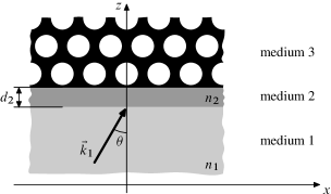
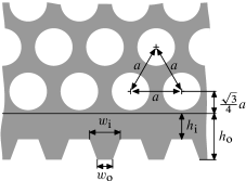
We begin by using the classical theory of AR coatings to calculate the refractive index and thickness of a single-layer coating that should minimize the reflection from the PC surface at a fixed angle of incidence and frequency . The value of should lie approximately midway the desired angular operation range of the final AR structure. Consider the system shown in fig. 4, in which a propagative plane wave with frequency and wave vector impinges from the dielectric 1 with refractive index on the surface of the homogeneous film 2 with thickness and refractive index coating the PC 3. Let us assume that medium 2 supports exactly one propagative diffraction order and is sufficiently thick for all the evanescent orders reflected from the PC surface to vanish at the interface between media 1 and 2. We can calculate the total amplitude of the reflected plane wave, , by summing up all the multiple reflections occurring in the system:
| (1) |
where and denote the amplitudes of the waves reflected from the interface between media and and transmitted through it, respectively, and with . The coefficients and are given by the Fresnel’s formulas,
| (2) |
with denoting the transverse immitance of medium normalised to the immitance of free space. For polarisation is defined as the transverse impedance of medium : . For polarisation, it is defined as the transverse admittance of the medium: . From eqs. (2) it immediately follows that and , hence
| (3) |
The parameters of the antireflection coating, and , can now be obtained by requiring the numerator of the fraction in the above equation to vanish. If the coating is lossless, so that , the numerator vanishes if and only if (i) the moduli of and are equal and (ii) the thickness is such that
| (4) |
where is an integer and stands for the argument of the complex number . Solving for , we get
| (5) |
It is usually best to choose the value of corresponding to the smallest positive admissible value of ; otherwise, internal resonances in the coating layer can spoil its antireflective properties for some angles of incidence.
We shall now use condition (i) to determine the refractive index of the AR coating. Substituting the Fresnel’s formulas (2) into the condition , we obtain
| (6) |
Straightforward algebra leads to
| (7) |
The - and -polarization cases need now to be considered separately. Assuming materials 1 and 2 to be nonmagnetic (), in the -polarization case we have
| (8) |
hence
| (9) |
It is easily seen that must be non-negative in order that be real, as we have assumed. For polarization,
| (10) |
This leads to the quadratic equation for ,
| (11) |
which has real solutions
| (12) |
provided that . It can be shown that this condition, together with the condition of real-valuedness of [for both solutions of eq. (12)], is fulfilled if and only if
| (13) |
In practice, there are further constraints on the choice of the constituent material of the coating. Other experimental issues aside, is bounded from below by the refractive index of air, and from above, by the index at which a second propagative diffraction order appears at the given value of . In appendix A it is shown how such constraints of the general form
| (14) |
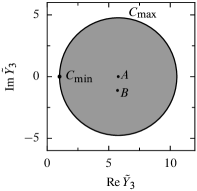
can be transformed into equivalent constraints on the immittance of the PC, . Let us denote by (, , ) the reduced immittances . It follows then that (14) holds if and only if one of the two following sets of conditions on is satisfied:
| (15) |
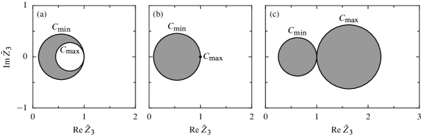
where stands for the half-plane and (, ) are the circles of radius centered at . The symbols and denote the interior and exterior of a region . To illustrate various possible geometries of the region of the complex plane determined by the constraints (14) transformed into the form (15), fig. 5 shows the shape of this region for polarization and three distinct choices of the parameters , , and .
Step 2
The coating obtained in step 1 is not practical, since its fabrication would call for integration of the PC with a completely different solid; moreover, a suitable material with the required value of refractive index might not be easily available. However, as noted in section II, a homogeneous thin film can often be replaced without adverse effects by a subwavelength grating: this is step 2. Such a grating could be easily etched in the same process as the underlying PC; it would then naturally be composed of the same materials as the PC, with permittivities, say, and ().
In order to calculate the fill factor of a binary lamellar grating mimicking a layer with refractive index obtained in the previous step, one can resort to the classical second-order effective-medium theory of gratings due to Rytov, described in ref. Raguin and Morris, 1993. According to this theory, the effective permittivity of a binary grating with period and fill factor (), composed of materials with permittivities and , and operating in the polarization is
| (16) |
where
| (17) |
For polarization, the effective permittivity is
| (18) |
where
| (19) |
and is given by eq. (17). Thus, the required fill factor can be obtained by setting or to in eq. (16) or (18) and solving it numerically for .
It should be noted that in the domain of validity of Rytov’s theory (small ) the functions and are monotonically increasing from to . Thus, a binary grating cannot simulate a material with permittivity outside the range delimited by the permittivities of the grating’s constituent materials. As a result, the bounds and mentioned in step 1 must fulfill and , respectively.
Step 3
The structure obtained at this stage should, in principle, ensure low reflectance for incidence angles close to . Nevertheless, owing to the applied approximations—neglect of higher diffraction orders excited by the PC and the AR grating—its geometrical parameters might not be precisely optimal. In addition, it is well known Raguin and Morris (1993, 1993) that trapezoidal and triangular AR gratings have larger angular and frequency tolerance than lamellar ones. Therefore, as step 3, it is advisable to apply a numerical optimization procedure to adjust the geometry of the grating, described by some small number of parameters, so as to minimize a given objective function . The geometry obtained in step 2 can be expected to provide a good starting point for a local search algorithm, such as the Nelder-Mead simplex method (ref. Press et al., 1992, section 10.4).
IV Application to a photonic crystal flat lens

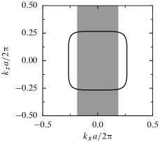
The first PC we shall consider is a hexagonal lattice of air holes of radius , where is the lattice constant, etched in a dielectric matrix of permittivity . These parameters correspond to the structure whose fabrication was reported in ref. Fabre et al., 2008. For polarization, at frequency , the effective refractive index can be attributed to the crystal, since its equifrequency contour (EFC) takes an approximately circular shape (fig. 6) with radius and group velocity directed inwards. (Information about the techniques used to obtain the numerical results discussed in this paper can be found in appendix B.)
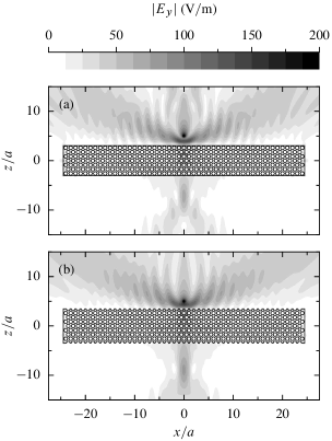
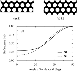
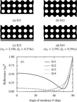
Veselago Veselago (1968) predicted that a slab of material with should act as a flat lens: an image of an object placed near one of the surfaces of the slab should be produced on the other side of the slab. Figure 7 shows the map of the modulus of the electric field generated by a wire source with current 1 A located above a slab of the PC in question. The parts (a) and (b) refer to slabs truncated in the ways shown in figs. 8(a) and (b), respectively; from now on, these two structures will be referred to as Semi-analytical design of antireflection gratings for photonic crystals and Semi-analytical design of antireflection gratings for photonic crystals. In accordance with the theoretical predictions, images are formed below the slabs. However, their amplitude is low (67 and 79 Vm for structures Semi-analytical design of antireflection gratings for photonic crystals and Semi-analytical design of antireflection gratings for photonic crystals, respectively) and intense beams reflected from the top of the lenses are visible in the upper part of the plots. This suggests that only a small fraction of energy is transmitted through the lenses. Indeed, as shown in fig. 8(a), the reflectance of structure Semi-analytical design of antireflection gratings for photonic crystals, , where is the specular reflection coefficient, exceeds 29% for all angles of incidence. Structure Semi-analytical design of antireflection gratings for photonic crystals performs better for low incidence angles, but degrades quickly with increasing . We shall now apply the algorithm presented in section III to design an AR grating for this PC, which ideally should function regardless of the angle of incidence.
As discussed in refs. Śmigaj and Gralak, 2008a and Śmigaj and Gralak, 2008b, the effective-medium model of PCs tends to be more accurate for crystals truncated along a plane with constant permittivity profile, as is the case, for instance, for structure Semi-analytical design of antireflection gratings for photonic crystals. Therefore in the first step of the design procedure we shall calculate the effective transverse impedance of this structure. We consider two ways of obtaining this quantity. First, we calculate it in the framework of the model presented in ref. Śmigaj and Gralak, 2008a using eq. (18) derived there. At frequency and angle of incidence (corresponding to ) we get and . We should now check whether lies within the region determined by the conditions (15) equivalent to the constraints (14) with and (the maximum index of a medium in which only a single propagative diffraction order exists). Figure 9, in which the value of cited above is marked with point , shows that this is indeed the case. Therefore eqs. (5) and (9) can be used to calculate the parameters of the AR coating of the crystal: refractive index and thickness . The geometry of this structure, called Semi-analytical design of antireflection gratings for photonic crystals from now on, is shown in fig. 10(a) and its reflectance is plotted in fig. 10(e) with a solid black line. It can be seen that the application of the coating reduces significantly the reflectance of the crystal, especially for small angles of incidence. However, the parameters of Semi-analytical design of antireflection gratings for photonic crystals are certainly not optimal, since its reflectance at the “design angle” is as large as 9%. This is due to the relatively large error introduced by the single-mode approximation for negative-refraction PC bands, as pointed out in ref. Śmigaj and Gralak, 2008a.
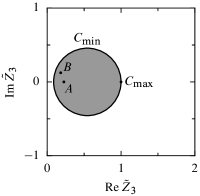
We shall evaluate, therefore, an alternative method of obtaining , which consists in calculating it directly from the rigorous specular reflection coefficient of the uncoated crystal at the chosen and . In other words, we assume that can be expressed in the form [cf. eq. (2)] and invert this formula to obtain . Of course, the effective impedance defined in this way depends on the material properties of medium 1. Nevertheless, at least for the PC in question, this dependence is weak for sufficiently small : we obtain for and the effective impedance does not change by more than 10% up to . As shown in fig. 9, the reduced impedance corresponding to the above value of (marked with point ) also lies within the allowed region of the plane. Taking this value of , from eqs. (5) and (9) we get and . The angular dependence of the reflectance of the PC covered with this coating, shown in fig. 10(b) and called Semi-analytical design of antireflection gratings for photonic crystals in the following, is plotted in fig. 10(e) with a solid gray line. It is evident that this structure has much better angular tolerance than Semi-analytical design of antireflection gratings for photonic crystals; moreover, its reflectance at is only 0.05%. Therefore we choose Semi-analytical design of antireflection gratings for photonic crystals as a basis for the further steps of the algorithm.
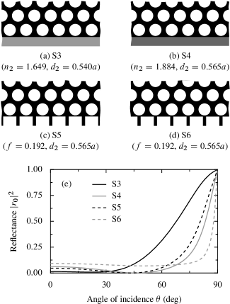
Numerical inversion of eq. (16) gives the fill factor of the binary grating mimicking a medium with . Since we would like the angular dependence of to be symmetric with respect to , the grating should be positioned so as to preserve the vertical mirror symmetry axes of the underlying PC. This can be done in two ways, shown in figs. 10(c) and (d). The reflectance of these two structures, called Semi-analytical design of antireflection gratings for photonic crystals and Semi-analytical design of antireflection gratings for photonic crystals, is plotted in fig. 10(e). Clearly, grating Semi-analytical design of antireflection gratings for photonic crystals reproduces fairly faithfully the original reflectance curve of the AR coating Semi-analytical design of antireflection gratings for photonic crystals. On the other hand, grating Semi-analytical design of antireflection gratings for photonic crystals behaves better in the high- region.
The lamellar gratings obtained in step 2 provide already a remarkable improvement over the uncoated PC and, in contrast to the AR coatings from step 1, should be manufacturable. Nevertheless, their geometry can be further ameliorated. To this end, as mentioned in the last paragraph of section III, we use the Nelder-Mead simplex algorithm to find the optimum values of the dimensions , , , and parametrising the trapezoidal grating shown in fig. 11. The objective function is defined as the average of the numerically calculated reflectance of the given structure over the desired angular tolerance interval ,
| (20) |
The integral in eq. (20) is calculated with the 20-point Gauss-Legendre quadrature algorithm (ref. Press et al., 1992, section 4.5), whose typical relative accuracy, , is better than that of the reflectance calculations, . The initial shape of the grating is taken to correspond to one of the lamellar gratings obtained in step 2, i.e., , , and . The search routine is terminated when the size of the simplex, defined as the average distance of its vertices from its geometric centre, falls below . The final values of the geometrical parameters of the grating are determined by selecting the best among the 16 structures obtained by rounding each of the parameters delivered by the simplex algorithm upwards or downwards to a multiple of .
Application of this procedure with , to grating Semi-analytical design of antireflection gratings for photonic crystals yields grating Semi-analytical design of antireflection gratings for photonic crystals shown in fig. 12(a). The plot in fig. 12(e) (solid black line) demonstrates the excellent antireflective properties of this structure (note the scale of the vertical axis). Its average reflectance is as low as 2.8%; in fact, does not exceed 5.5% until . The structure does not seem to present special fabrication difficulties—e.g., acute angles—except possibly for the relatively thin dielectric veins separating the circular holes from the surface. Should this pose a real experimental difficulty, one can increase the value of at the expense of a slight performance deterioration. For example, grating Semi-analytical design of antireflection gratings for photonic crystals with [fig. 12(b)] has average reflectance of 4.8%.
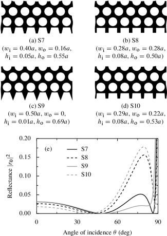
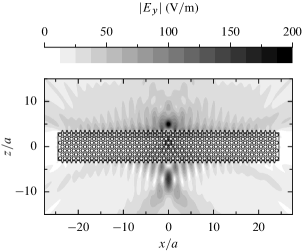
Figure 13 shows the map of the modulus of the electric field produced by a point source placed above a PC slab coated with AR gratings of type Semi-analytical design of antireflection gratings for photonic crystals from above and below. The comparison with fig. 7 reveals the significant improvement brought about by the AR grating: not only are the reflected beams prominent in the upper part of the latter figure suppressed, but the amplitude of the image formed by the lens grows to 159 Vm, which is two times better than in the situation from fig. 7(b).
Optimization of structure Semi-analytical design of antireflection gratings for photonic crystals leads to gratings with average reflectance comparable to that of Semi-analytical design of antireflection gratings for photonic crystals and Semi-analytical design of antireflection gratings for photonic crystals but composed of “narrower” trapezoids (), thus less suitable for fabrication. Therefore we omit the detailed discussion of these structures.
As a complement, we mention that in refs. Śmigaj et al., 2009a and Śmigaj et al., 2009b two other trapezoidal AR gratings, here denoted Semi-analytical design of antireflection gratings for photonic crystals and Semi-analytical design of antireflection gratings for photonic crystals, were presented. Their geometrical parameters, shown in figs. 12(c) and (d), were obtained by minimizing the objective function (average modulus of the specular reflection coefficient ) calculated with a less accurate quadrature algorithm. The average reflectance of structure Semi-analytical design of antireflection gratings for photonic crystals in the full – range, 2.8%, matches that of Semi-analytical design of antireflection gratings for photonic crystals; in a more restricted range, say, –, the performance of grating Semi-analytical design of antireflection gratings for photonic crystals is even slightly better. Nonetheless, its disadvantage lies in the presence of very thin dielectric veins at the surface. Grating Semi-analytical design of antireflection gratings for photonic crystals, with , is devoid of this problem. However, it is superseded by structure Semi-analytical design of antireflection gratings for photonic crystals with identical , which has somewhat lower average reflectance.
Finally, a word about tolerance to fabrication imperfections. A fabrication process invariably perturbs the geometrical parameters of the manufactured structure. To assess the sensitivity of the proposed gratings to fabrication errors, we have determined the maximum perturbation of each of the four geometrical parameters of grating Semi-analytical design of antireflection gratings for photonic crystals for which the grating’s average reflectance in the angular range did not exceed 5%. Three values of were considered: , , and . The results of this test are summarized in table 1. It can be seen that the grating is more sensitive to variations of the height of the trapezoids (via the and parameters) than of their width ( and ). The constraints for and are rather stringent and unlikely to be met in practice. In contrast, fabrication of a structure satisfying the constraints for seems well within reach of current technology. We have also tested the frequency tolerance of grating Semi-analytical design of antireflection gratings for photonic crystals, finding that the its average reflectance stays below 5% for (), (), and (). This tolerance seems quite sufficient for applications related to lensing.
| – (22 nm) | – (9 nm) | – (5 nm) | – (7 nm) | |
| – (63 nm) | – (26 nm) | – (14 nm) | – (19 nm) | |
| – (162 nm) | – (59 nm) | – (39 nm) | – (42 nm) |
V Application to a supercollimating photonic crystal
The second example to be considered is a PC composed of a square lattice of air holes of radius , where is the lattice constant, etched in a dielectric matrix of permittivity . Near the frequency its EFCs for polarization take a square-like shape (cf. fig. 14). In consequence, supercollimated beams Kosaka et al. (1998); Prather et al. (2007) can propagate in the crystal.
The solid and dashed black curves in fig. 15(e) show the angular dependence of the reflectance of this PC at and for two different truncation planes, corresponding to the structures shown in figs. 15(a)–(b) and called Semi-analytical design of antireflection gratings for photonic crystals and Semi-analytical design of antireflection gratings for photonic crystals in the following. It is seen that the crystal cut through hole centers has fairly low reflectance: about 10% at normal incidence and decreasing for larger angles up to . This level of power losses might in fact be already sufficient for practical applications. Nevertheless, for the sake of illustration, we shall present the design procedure of AR gratings that help to decrease even further the reflectance of the PC in question.
Here, we are mostly interested in coupling the incoming light to modes lying on the flat horizontal part of the PC’s EFC. As shown in fig. 14, at frequency this corresponds roughly to the range , i.e., . Therefore we choose as the design angle of the AR coating. As in the previous section, we test two different ways of calculating the effective immittance (in this case, admittance) of the crystal cut along a constant-permittivity plane, i.e., structure Semi-analytical design of antireflection gratings for photonic crystals. The effective-medium model presented in ref. Śmigaj and Gralak, 2008a yields . In turn, the effective admittance calculated from the rigorous reflection coefficient of structure Semi-analytical design of antireflection gratings for photonic crystals embedded in air is . Figure 16 shows that the reduced admittances corresponding to both these values lie within the region of the complex plane determined by the conditions (15) equivalent to the constraints (14) with , (the refractive index for which the second propagative diffraction order appears) and . The parameters of the AR coatings determined from these two values of are (, ) and (, ), respectively. Figures 15(c)–(d) show the geometry of these coatings, henceforth referred to as Semi-analytical design of antireflection gratings for photonic crystals and Semi-analytical design of antireflection gratings for photonic crystals, whereas the angular dependence of their reflectance is plotted with solid and dashed gray lines in fig. 15(e). As in the PC lens case, the AR coating Semi-analytical design of antireflection gratings for photonic crystals designed using the value of obtained from the rigorous reflection coefficient of the crystal performs slightly better than the other one. Therefore structure Semi-analytical design of antireflection gratings for photonic crystals shall be used in the subsequent design step.
From numerical inversion of eq. (18) it follows that the fill factor of the binary grating mimicking a medium with for polarization is . Figures 17(a)–(b) show the geometry of the two gratings, called Semi-analytical design of antireflection gratings for photonic crystals and Semi-analytical design of antireflection gratings for photonic crystals, with this fill factor and a mirror symmetry plane perpendicular to the direction of periodicity. From the juxtaposition of their reflectance curves [fig. 17(c)] it follows that structure Semi-analytical design of antireflection gratings for photonic crystals has somewhat better performance than Semi-analytical design of antireflection gratings for photonic crystals. In fact, there is some similarity between the geometry of grating Semi-analytical design of antireflection gratings for photonic crystals and the truncated crystal Semi-analytical design of antireflection gratings for photonic crystals, which also exhibited fairly low reflectance: the surface of both these structures contains “teeth” shifted by in the horizontal direction with respect to the positions of the circular holes. Therefore, one could view the crystal Semi-analytical design of antireflection gratings for photonic crystals as an imperfect realization of the AR grating Semi-analytical design of antireflection gratings for photonic crystals.
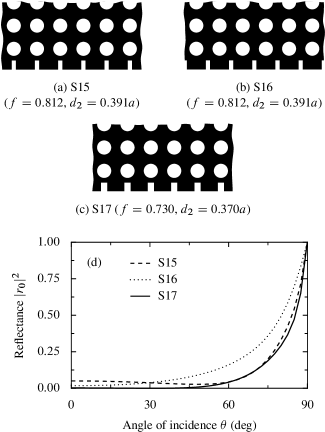
The lamellar grating Semi-analytical design of antireflection gratings for photonic crystals can be further ameliorated by adjusting its thickness and fill factor to minimize the objective function defined in eq. (20). We take , and, as before, perform the optimization with the Nelder-Mead simplex algorithm. This leads to structure Semi-analytical design of antireflection gratings for photonic crystals with and , shown in fig. 17(c). Its reflectance curve is plotted in fig. 17(d) (solid line). In the angular range , the reflectance never exceeds 0.6%, on average amounting to only 0.12%. The structure does not seem to present any special fabrication problems. It is possible to continue the grating’s optimization by allowing it to take a trapezoidal rather than a lamellar shape; however, in view of its already very good AR properties, this appears unnecessary.
VI Application to a non-reciprocal mirror
In this section, the procedure is applied to a unidirectional mirror similar to that proposed in ref. Vanwolleghem et al., 2009. This device has the form of a slab of the PC shown in the inset of fig. 18(a). The PC consists of a hexagonal lattice of non-centrosymmetric motifs etched in a magneto-optical matrix characterized by a gyrotropic permittivity tensor
| (21) |
The presence of this magneto-optical material lifts the time-reversal symmetry of Maxwell’s equations. Since the spatial inversion symmetry is also broken, the crystal becomes nonreciprocal: the usual property of the dispersion relation, (ref. Sakoda, 2001, pp. 22–23), no longer holds. The -polarization EFC of this crystal at frequency is shown in fig. 18(a). It can be seen that plane waves impinging at the angle of about (corresponding to ) on the bottom surface of a slab made from this PC will be coupled to its propagative mode, and thus will be partially transmitted. However, waves travelling in the opposite direction, incident from the top, will be totally reflected, since the crystal has no propagative modes with . This behaviour justifies the name unidirectional mirror. The problem with the presented device is its large forward loss: even waves propagating in the “allowed” direction undergo a significant reflection on the surfaces of the slab. This can be seen in fig. 18(b), where the reflectance curve of the crystal truncated as in fig. 18(a) is juxtaposed with the relevant fragment of the EFC. Clearly, to be useful in practice, the unidirectional mirror needs to be coated with some AR structure.
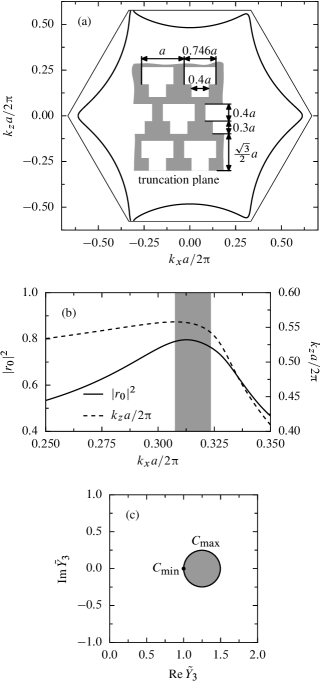
Unfortunately, the design of an appropriate AR grating using the procedure described in section III turns out to be impossible. For instance, at , near the centre of the region where the unidirectional mirroring effect occurs, the reflection coefficient of the uncoated PC is , which corresponds to . As evidenced by fig. 18(d), this lies far outside the region of the complex plane determined by the conditions (15) equivalent to the constraints (14) with and (the refractive index of the most optically dense coating in which the second propagative diffraction order would not yet appear). In fact, if we blindly apply eqs. (7) and (12) to calculate the refractive index of the optimum AR coating, we obtain or . It is obvious that none of these indices can be simulated by any binary grating composed of the constituent materials of the PC. Therefore, an AR structure for the unidirectional mirror will probably need to be designed with some purely numerical method. In particular, Lawrence et al. Lawrence et al. (2009) have shown their approach to give good results for a superprism that, uncoated, has an extremely high reflectance ().
VII Evanescent waves regime
The behaviour of evanescent waves is approached through the example of the photonic crystal flat lens described in section IV. In that case, the amplification of these waves is of vital importance to obtain subwavelength resolution Pendry (2000). In a photonic crystal flat lens, two mechanisms may lead to an amplification of evanescent waves Luo et al. (2003): the single interface resonances and the overall resonances (see ref. Luo et al., 2003 for discussion in detail). While the first mechanism is actually involved in the original flat lens, the solely second mechanism has been investigated. This situation can be changed thanks to the new models introduced recently Śmigaj and Gralak (2008a); Lawrence et al. (2009); Śmigaj et al. (2011) and based on reflectivity on semi-infinite crystals.
The present approach is based on the following conjecture: assuming that a nearly constant effective index is obtained over all the range of wavevectors corresponding to propagative waves, it can be expected that this remains true when this range is continued in the evanescent regime. For instance, this behaviour has already been observed in multilayers Pierre and Gralak (2008). For the photonic crystal flat lens, the refractive index is close to at (from the dispersion law of Fig. 6) and, with the AR grating, it can be considered that the effective index is nearly for the range of propagating waves. Now, if the effective index remains nearly for evanescent waves, then it can be expected that single-interface resonances are present around the working frequency .
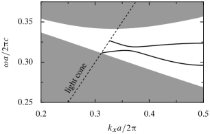
Fig. 19 shows the single-interface resonances of structure Semi-analytical design of antireflection gratings for photonic crystals below the light cone. It is observed that the dispersion curve of these resonances starts from the intersection between the bands of the bulk PC and the the light cone at . This shows that the effective index has no jump from propagative to evanescent waves, and thus confirms the conjecture proposed above, as well as the result found in ref. Pierre and Gralak, 2008 in the one-dimensional case. To our knowledge, no model can predict this continuity of the effective index at this change of regime. This might be a subject for furter investigations.
VIII Conclusion
In this article we have presented a new method of designing gratings that, superimposed on surfaces of PCs crystals, will minimize their reflectance. The design algorithm consists of three steps. First, the parameters of a homogeneous-layer AR coating are calculated from an effective-medium approximation of the PC in question. Second, an analytical effective-medium theory of gratings is used to find the parameters of a binary lamellar grating composed solely of the constituent materials of the crystal and approximating the coating obtained in the previous step. Third, the shape of the grating is refined with a numerical local-search routine so as to minimize the reflectance of the structure in the desired angular or frequency range. This last step is necessary owing to the approximations made in the analytical derivations used in the first two steps of the procedure.
This algorithm of AR grating design can be viewed as complementary to the method proposed by Lawrence et al. Lawrence et al. (2008, 2009). While their approach is based on an exhaustive scan of the whole parameter space (made very efficient by the application of the matrix-valued effective immittance of gratings), ours rests on approximate analytical considerations used to find a starting point for a local search procedure.
The proposed method has been applied to three example crystals with EFCs of different curvature: a supercollimating crystal with a very flat EFC, a crystal exhibiting negative refraction, with almost circular EFC, and a PC superprism, whose EFC has a kink. In the two first cases, the design process succeeded in producing AR gratings ensuring very low reflectance in a wide angular range. The obtained structures are quite compact and apparently rather straightforward to fabricate. In the last case, the procedure broke down owing to the violation of the constraints (15) on the effective immittance of the crystal that must be satisfied in order that the AR coating produced in the first step can be approximated with a binary grating made of realistic materials. The existence of these constraints is the basic limitation of the presented procedure.
Appendix A Constraints on
We begin by noting that the conditions (14) can always be rewritten in the form
| (22) |
with appropriate and . Specifically, for polarization, the formulas for and follow readily from eq. (9):
| (23) |
For polarization, due to the more complex form of eq. (12) and the presence of the supplementary condition (13), several cases must be considered. The final formulas for and are given in table 2.
Appendix B Numerical methods
A word about the different methods used for the numerical simulations presented in this article. Almost all the calculations whose results are presented in sections IV and VII have been made with the differential method Vincent (1980); Popov and Bozhkov (2000); Nevière and Popov (2002); Śmigaj (2007). The exceptions are the field maps shown in figs. 7 and 13, produced with the finite-element method using the RF module of the COMSOL package. The numerical results reported on in section V have been obtained with the finite-difference frequency-domain method. Finally, the simulations of the magneto-optical PC discussed in section VI have been made with a code based on the Fourier modal method Moharam et al. (1995) and implementing the factorisation rules for anisotropic materials derived in ref. Popov and Nevière, 2001.
References
- Notomi (2000) M. Notomi, Phys. Rev. B 62, 10696 (2000).
- Pendry (2000) J. B. Pendry, Phys. Rev. Lett. 85, 3966 (2000).
- Gralak et al. (2000) B. Gralak, S. Enoch, and G. Tayeb, J. Opt. Soc. Am. A 17, 1012 (2000).
- Enoch et al. (2003) S. Enoch, G. Tayeb, and B. Gralak, IEEE Trans. Antennas Propag. 51, 2659 (2003).
- Gralak et al. (2006) B. Gralak, S. Enoch, and G. Tayeb, in Metamaterials: physics and engineering explorations, edited by N. Engheta and R. W. Ziolkowski (Wiley, New York, 2006), chap. 10, pp. 261–283.
- Wang and Fan (2005) Z. Wang and S. Fan, Appl. Phys. B 81, 369 (2005).
- Śmigaj et al. (2010) W. Śmigaj, J. Romero-Vivas, B. Gralak, L. Magdenko, B. Dagens, and M. Vanwolleghem, Opt. Lett. 35, 568 (2010).
- Dobrowolski et al. (2002) J. A. Dobrowolski, D. Poitras, P. Ma, H. Vakil, and M. Acree, Appl. Opt. 41, 3075 (2002).
- Grann and Moharam (1996) E. B. Grann and M. G. Moharam, J. Opt. Soc. Am. A 13, 988 (1996).
- Macleod (2001) H. A. Macleod, Thin-film optical filters (Institute of Physics, Bristol, 2001).
- Orfanidis (2008) S. J. Orfanidis, Electromagnetic waves and antennas, http://www.ece.rutgers.edu/~orfanidi/ewa (2008).
- Bräuer and Bryngdahl (1994) R. Bräuer and O. Bryngdahl, Appl. Opt. 33, 7875 (1994).
- Raguin and Morris (1993) D. H. Raguin and G. M. Morris, Appl. Opt. 32, 1154 (1993).
- Raguin and Morris (1993) D. H. Raguin and G. M. Morris, Appl. Opt. 32, 2582 (1993).
- Kikuta et al. (2003) H. Kikuta, H. Toyota, and W. Yu, Opt. Rev. 10, 63 (2003).
- Xiao et al. (2004) S. Xiao, M. Qiu, Z. Ruan, and S. He, Appl. Phys. Lett. 85, 4269 (2004).
- Botten et al. (2006) L. C. Botten, T. P. White, C. M. de Sterke, and R. C. McPhedran, Phys. Rev. E 74, 026603 (2006).
- Li et al. (2007) Z. Li, E. Ozbay, H. Chen, J. Chen, F. Yang, and H. Zheng, J. Phys. D 40, 5873 (2007).
- Lee et al. (2008) S.-G. Lee, J.-S. Choi, J.-E. Kim, H.-Y. Park, and C.-S. Kee, Opt. Express 16, 4270 (2008).
- Park et al. (2009) J.-M. Park, S.-G. Lee, H. Y. Park, J.-E. Kim, and M.-H. Lee, J. Opt. Soc. Am. B 26, 1967 (2009).
- Jin and He (2007) Y. Jin and S. He, Phys. Lett. A 360, 461 (2007).
- Zhang and Li (2007) B. Zhang and M. Y. Li, Eur. Phys. J. D 45, 321 (2007).
- Baba and Ohsaki (2001) T. Baba and D. Ohsaki, Jpn. J. Appl. Phys. 40, 5920 (2001).
- Baba et al. (2004) T. Baba, T. Matsumoto, and M. Echizen, Opt. Express 12, 4608 (2004).
- Matsumoto et al. (2005) T. Matsumoto, S. Fujita, and T. Baba, Opt. Express 13, 10768 (2005).
- Matsumoto et al. (2006) T. Matsumoto, K. Eom, and T. Baba, Opt. Lett. 31, 2786 (2006).
- Lawrence et al. (2008) F. J. Lawrence, L. C. Botten, K. B. Dossou, and C. M. de Sterke, Appl. Phys. Lett. 93, 121114 (2008).
- Lawrence et al. (2009) F. J. Lawrence, L. C. Botten, K. B. Dossou, C. M. de Sterke, and R. C. McPhedran, Phys. Rev. A 80, 023826 (2009).
- Witzens et al. (2004) J. Witzens, M. Hochberg, T. Baehr-Jones, and A. Scherer, Phys. Rev. E 69, 046609 (2004).
- Momeni and Adibi (2005) B. Momeni and A. Adibi, Appl. Phys. Lett. 87, 171104 (2005).
- Press et al. (1992) W. H. Press, B. P. Flannery, S. A. Teukolsky, and W. T. Vetterling, Numerical recipes in C (Cambridge University Press, 1992).
- Fabre et al. (2008) N. Fabre, L. Lalouat, B. Cluzel, X. Mélique, D. Lippens, F. de Fornel, and O. Vanbésien, Phys. Rev. Lett. 101, 073901 (2008).
- Vincent (1980) P. Vincent, in Electromagnetic theory of gratings, edited by R. Petit (Springer, Berlin, 1980), chap. 4, pp. 101–122.
- Popov and Bozhkov (2000) E. Popov and B. Bozhkov, Appl. Opt. 39, 4926 (2000).
- Nevière and Popov (2002) M. Nevière and E. Popov, Light propagation in periodic media. Differential theory and design (Marcel Dekker, New York, 2002).
- Śmigaj (2007) W. Śmigaj, Master’s thesis, Faculty of Physics, Adam Mickiewicz University in Poznań (2007).
- Veselago (1968) V. G. Veselago, Sov. Phys. Usp. 10, 509 (1968).
- Śmigaj and Gralak (2008a) W. Śmigaj and B. Gralak, Phys. Rev. B 77, 235445 (2008a).
- Śmigaj and Gralak (2008b) W. Śmigaj and B. Gralak, Proc. SPIE 6987, 698726 (2008b).
- Śmigaj et al. (2009a) W. Śmigaj, B. Gralak, R. Pierre, and G. Tayeb, in SPP4 Surface Plasmon Photonics Conference (2009a).
- Śmigaj et al. (2009b) W. Śmigaj, B. Gralak, R. Pierre, and G. Tayeb, Opt. Lett. 34, 3532 (2009b).
- Kosaka et al. (1998) H. Kosaka, T. Kawashima, A. Tomita, M. Notomi, T. Tamamura, T. Sato, and S. Kawakami, Phys. Rev. B 58, R10096 (1998).
- Prather et al. (2007) D. W. Prather, S. Shi, J. Murakowski, G. J. Schneider, A. Sharkawy, C. Chen, B. L. Miao, and R. Martin, J. Phys. D 40, 2635 (2007).
- Vanwolleghem et al. (2009) M. Vanwolleghem, X. Checoury, W. Śmigaj, B. Gralak, L. Magdenko, K. Postava, B. Dagens, P. Beauvillain, and J.-M. Lourtioz, Phys. Rev. B 80, 121102(R) (2009).
- Sakoda (2001) K. Sakoda, Optical properties of photonic crystals (Springer, Berlin, 2001).
- Luo et al. (2003) C. Luo, S. G. Johnson, J. D. Joannopoulos, and J. B. Pendry, Phys. Rev. B 68, 045115 (2003).
- Śmigaj et al. (2011) W. Śmigaj, P. Lalanne, J. Yang, T. Paul, C. Rockstuhl, and F. Lederer, Appl. Phys. Lett. 98, 111107 (2011).
- Pierre and Gralak (2008) R. Pierre and B. Gralak, J. Mod. Opt. 55, 1759 (2008).
- Moharam et al. (1995) M. G. Moharam, E. B. Grann, D. A. Pommet, and T. K. Gaylord, J. Opt. Soc. Am. A 12, 1068 (1995).
- Popov and Nevière (2001) E. Popov and M. Nevière, J. Opt. Soc. Am. A 18, 2886 (2001).