Electrical conduction processes in ZnO in a wide temperature range 20–500 K
Abstract
We have investigated the electrical conduction processes in as-grown and thermally cycled ZnO single crystal as well as as-grown ZnO polycrystalline films over the wide temperature range 20–500 K. In the case of ZnO single crystal between 110 and 500 K, two types of thermal activation conduction processes are observed. This is explained in terms of the existence of both shallow donors and intermediately deep donors which are consecutively excited to the conduction band as the temperature increases. By measuring the resistivity of a given single crystal after repeated thermal cycling in vacuum, we demonstrate that oxygen vacancies play an important role in governing the shallow donor concentrations but leave the activation energy (272 meV) largely intact. In the case of polycrystalline films, two types of thermal activation conduction processes are also observed between 150 and 500 K. Below 150 K, we found an additional conduction process due to the nearest-neighbor-hopping conduction mechanism which takes place in the shallow impurity band. As the temperatures further decreases below 80 K, a crossover to the Mott variable-range-hopping conduction process is observed. Taken together with our previous measurements on of ZnO polycrystalline films in the temperature range 2–100 K [Y. L. Huang et al., J. Appl. Phys. 107, 063715 (2010)], this work establishes a quite complete picture of the overall electrical conduction mechanisms in the ZnO material from liquid-helium temperatures up to 500 K.
pacs:
72.20.My, 71.30.Tm, 73.50.JtI Introduction
Zinc oxide (ZnO) is a wide band gap semiconductor with a direct energy gap of 3.4 eV at room temperature. This class of material is usually unintentionally (or, natively) doped with n-type impurities, such as oxygen vacancies, Zn interstitials, and impurity hydrogen atoms. However, the exact doping behavior of different types of unintentional and intentional (e.g., group I or group III) dopants is still under much theoretical and experimental debate. Janotti09 ; McCluskey09 ; Ozgur05
ZnO has recently attracted intense attention owing to its potential prospects in optoelectronic applications. Ellmer08 ; LiZQ06 ; Look01 Compared with the widely studied optical properties, the electrical conduction processes in ZnO materials (single crystals, polycrystalline films, etc.) have not much been investigated over a wide range of temperature. Kumar08 ; Tiwari04 ; Heluani06 ; Tsurumi99 Physically, the measurements on the temperature dependence of resistivity, , can provide very useful information on the carrier transport mechanisms as well as the associated impurity levels and their distributions in energy in a given semiconducting material. Recently, Huang et al. Huang10 have investigated the electrical conduction processes in a series of oxygen deficient polycrystalline ZnO films (1 m thick) in the temperature range 2–100 K. They observed the three-dimensional Mott variable-range-hopping (VRH) conduction process below 100 K. As the temperature further decreased below 25 K, a crossover to the Efros-Shklovskii VRH conduction process was found. These two types of VRH conduction processes in ZnO films have been successfully explained in a coherent manner. On the other hand, the charge transport properties above 100 K has not been explicitly addressed in that work, due to the lacking of data above 300 K. In this work, we aim at extending the measurements on to temperatures up to 500 K in order to further unravel the overall electrical conduction mechanisms in ZnO, especially at 100 K. We have measured an as-grown ZnO single crystal and remeasured the series of as-grown ZnO polycrystalline films which were first studied in Ref. Huang10, . The as-grown single crystal has been repeatedly thermally cycled in vacuum and their has been measured during each thermal cycling process. The polycrystalline films had been deposited in different oxygen atmospheres to contain different amounts of oxygen vacancies so that they possessed differing shallow donor concentrations when as prepared. Our new results are reported below.
We would like to emphasize that all the measurements reported in this study have been carried out in a vacuum ( torr) and in a “dark” environment without involving any photo-induced carriers. Therefore, complex thermal annealing effects which might result from resistivity measurements performed in, e.g., an air (or an active gas) atmosphere at highly elevated temperatures, Zhang04 can be safely avoided.
This paper is organized as follows. In Sec. II, we briefly discuss our experimental method for sample fabrication and resistance measurements. Our results of the temperature dependence of resistance in the wide temperature interval 20–500 K and their physical interpretations are presented in Sec. III. Section IV contains our conclusion as well as a summary of the overall electrical conduction mechanisms in the ZnO materials.
II Experimental Method
Our ZnO single crystal (2.521.940.45 mm3) were grown by the hydrothermal method and was obtained from a commercial supplier. supplier Unfortunately, the detailed growth conditions were unavailable. However, the data do provide us meaningful information on the carrier transport processes in the ZnO material (see below). This as-grown crystal has a room temperature resistivity of 5.45 cm. Our ZnO polycrystalline films were fabricated by the standard rf sputtering deposition method on glass substrates. The starting ZnO target was of 99.99% purity, and the glass substrates were held at 550∘C during the deposition process. The films were deposited in varying mixtures of argon and oxygen gases. The of these films had previously been measured and discussed by Huang et al. Huang10 for 100 K.
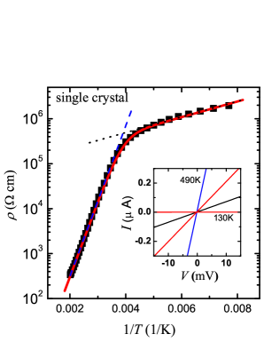
In this work, four-probe resistance measurements were carried out using a Keithley Model K-6430 as a current source and a high-impedance (T) Keithley Model K-617 as a voltmeter. The samples were mounted on the sample holder which was situated inside a stainless vacuum can in a JANIS CCS350 closed-cycle refrigerator (10–500 K). The working pressure in the vacuum can was torr throughout all resistivity measurement processes, whether the vacuum can was connected to a diffusion pump (at 250 K) or not (at 250 K, see below for further discussion). Moreover, the stainless vacuum can contained no optical windows, and thus our measurements were performed in the dark, i.e., this experiment did not invoke any kind of photo-induced currents. The four-terminal current leads and voltage leads (pogo pins) were attached to the samples with the aid of silver paste. It should be noted that the resistances reported in this work were all measured by scanning the current-voltage (I-V) characteristics at various fixed temperatures between 20 and 500 K. The resistance at a given temperature was determined from the regime around the zero bias voltage, where the I-V curve was linear. In fact, our I-V curves in every sample were linear over a wide range of bias voltage. The inset of Fig. 1 shows the linear - characteristics of the as-grown ZnO single crystal at four representative temperatures, as indicated in the caption to Fig. 1.
III Results and discussion
III.1 ZnO single crystal: thermal activation conduction over 110–500 K
Figure 1 plots the measured resistivity as a function of reciprocal temperature for the as-grown single crystal between 110 and 500 K. (The resistance below 110 K became too large to be accurately measured.) Two distinct slopes are explicitly seen in the two different temperature regimes of 110–220 K (straight dotted line) and 290–500 K (straight dashed line), respectively. Such Arrhenius-type behavior immediately suggests that the responsible charge transport arises from the thermal activation conduction processes. Indeed, we found that our measured data can be quantitatively described by the equation
| (1) |
where and are temperature insensitive resistivity prefactors, and and are the relevant activation energies associated with the two kinds of thermal activation conduction processes. is the Boltzmann constant. In Fig. 1, the solid curve is a least-square fit to Eq. (1). It clearly manifests that Eq. (1) can well describe the experimental result. Our fitted values of , , , and are listed in Table I. This observation illustrates that there exist in the as-grown single crystal a group of shallow donors with an activation energy of 29 meV and a group of intermediately deep donors with an activation energy of 330 meV. (In this work, we shall maintain the convention .) At the sufficiently high measurement temperatures of 290 K, both the shallow and the intermediately deep donors are excited to the conduction band and are responsible for the electrical transport. However, the exponential temperature dependence of is mainly governed by the number of those intermediately deep donors which are being excited to the conduction band (the so-called -conduction channel). As reduces below 220 K, the intermediately deep donors become essentially intact while the shallow donors can still be readily excited to the conduction band. The dependence of is thus largely determined by the number of those shallow donors being excited to the conduction band (the so-called -conduction channel). In short, Eq. (1) represents the “band conduction” processes.
| single crystal | (300 K) ( cm) | ( cm) | (meV) | ( cm) | (meV) |
|---|---|---|---|---|---|
| as-grown | 5.45 | 0.144 | 334 | 1.47 | 29.2 |
| first-cycled | 4.56 | 0.154 | 330 | 2.50 | 28.1 |
| second-cycled | 2.70 | 0.145 | 332 | 1.72 | 24.7 |
| third-cycled | 2.01 | 0.125 | 337 | 1.02 | 26.4 |
It should be noted that our extracted and values are in good accord with the corresponding activation energies previously obtained by Look Look01 (340 meV), Wenckstern et al. Wenckstern07 (34–37 and 300–370 meV), and Schifano et al. Schifano09 (30, 50, and 290 meV) in various ZnO single crystals and in different temperature intervals. Recently, in a series of single-crystalline ZnO nanowires, Chiu et al. Chiu09 (Tsai et al. Tsai10 ) have also reported an activation energy of 30–40 (25) meV. In other words, we may conclude that different ZnO single crystals grown by differing methods and under differing conditions possess essentially similar types of shallow and intermediately deep donor levels. (Obviously, the donor concentrations would vary from experiment to experiment.)
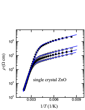
In Fig. 2, we plot our measured resistivities as a function of reciprocal temperature for the as-grown and then repeatedly thermally cycled single crystal. The closed squares (taken from Fig. 1), open squares, closed circles, and open circles represent the as-grown, first-cycled, second-cycled, and third-cycled samples, respectively. In practice, our data for every sample were measured from 500 K down. The sample was placed in the dark vacuum can and first heated to 500 K. The dependence of was then measured with progressive lowing of temperature. During the data acquisition process from 500 K down to 250 K, the dark vacuum can was connected to a diffusion pump for continuous pumping. The diffusion pump was disconnected when the temperature reached 250 K. backflow Such a measurement process (which lasted for 270 min between 250 and 500 K) had effectively served as a “thermal annealing” (in vacuum) process. Therefore, the oxygen contain in the sample was reduced from that in the previous run. In other words, the amount of oxygen vacancies increased, leading to a decrease in the sample resistivity. We have repeated the measurements in the temperature interval 110–500 K for four times, and denoted the sample by as-grown, first-cycled, second-cycled, and third-cycled samples, as mentioned.
Inspection of Fig. 2 indicates that, in the temperature interval 330–500 K, the data collapse closely onto a straight line. On the other hand, below 330 K, the measured data systematically decrease after each repeated thermal cycling. Quantitatively, the resistivity ratios of the as-grown sample to the third-cycled sample are 1.0 at 460 K, 2.7 at 300 K, and 11 at 220 K. This variation in resistivity ratio suggests that the rich amount of the intermediately deep donors rich and their associated activation energies, i.e., the values, are barely affected by our measuring and/or thermal cycling process. This is expected, since the activation energies associated with these donor levels are comparatively large while our thermal cycling temperature is relatively low.
What is more interesting is the behavior of between 110 and 220 K. While the value at a given decreases with repeated thermal cycling as mentioned, the temperature dependence of maintains essentially unchanged. Numerically, our least-squares fitted slopes, i.e., the values, in this temperature interval vary only by 10%, see Table I. This quantitative result is meaningful. It strongly implies that the amount of oxygen vacancies, namely, the shallow donor concentration, in the sample is increased after each repeated thermal cycling. Nevertheless, the thermal activation energy, namely, the shallow donor level below the conduction band minimum, remains essentially unchanged. (See Ref. disperse, for a brief discussion on the thermal-cycling-induced weak dispersion of the shallow donor energy levels.) This observation is strongly supportive of the important roles of oxygen vacancies as the shallow donors in ZnO. On the theoretical side, based on the formation energy consideration, it has recently been argued that oxygen vacancies would form negative-U centers, rather than shallow donors, in the ZnO material. Janotti05 ; Vlasenko05 ; Zhang01 ; Lany05 This theoretical prediction is not supported by the present result, Fig. 2. This puzzling issue requires further clarification.
III.2 ZnO polycrystalline films
III.2.1 Thermal activation conduction and nearest-neighbor-hopping conduction: 90–500 K
Figure 3 shows the variation in the logarithm of resistivity with reciprocal temperature for four ZnO polycrystalline films between 90 and 500 K, as indicated. In sharp contrast to the case of single crystal (Fig. 2), Fig. 3 clearly reveals that smoothly increases with decreasing temperature. That is, there does not exist a visible straight regime in any temperature interval in the log–(1/) plot from 500 down to 90 K. Quantitatively, we found that these results can not be described by Eq. (1). Instead, they can be described by the following equation
| (2) |
where , , , and have the similar meaning as defined in Eq. (1). The third term on the right hand side represents a new, additional electrical conduction channel which is characterized by a temperature insensitive resistivity prefactor and a thermal activation energy . (In the following discussion, we shall maintain the convention .)
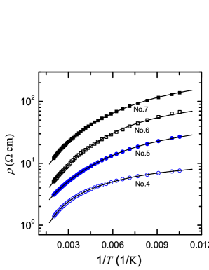
Our fitted results with Eq. (2) are plotted as the solid curves in Fig. 3 and the values of the adjustable parameters are listed in Table II. We obtain the thermal activation energies 113–135 meV, 26–39 meV, and 2.3–5.7 meV. The three types of conduction processes dominate the dependence of in the temperature intervals of 400–500 K (the -conduction channel), 150–400 K (the -conduction channel), and 90–150 K (the -conduction channel). Physically, the - and the -conduction processes are just those described in the above subsection. However, the activation energy is markedly reduced from 330 meV for single crystal to 12510 mev for polycrystalline films (see further discussion below). The additional -conduction channel can be ascribed to the nearest-neighbor-hopping (NNH) conduction mechanism which takes place in the shallow “impurity band.” That is, as the temperature decreases below 150 K, even the shallow donors (not mentioning the intermediately deep donors) can no longer be effectively excited to the conduction band. The charge transport is then largely governed by those electrons which hop from an occupied state (which lies below the Fermi energy) to an unoccupied nearest-neighbor state (which lies above the Fermi energy) in the impurity band. Such a hopping process is phonon assisted and requires a small amount of energy, i.e., the thermal activation energy. It should be noted that a shallow impurity band can form in the oxygen deficient ZnO polycrystalline films but not in the ZnO single crystal, because the former samples contain far higher amounts of oxygen vacancies. A large amount of oxygen vacancies causes a notable dispersion of the donor levels or ionization energies, and thus forming an impurity band. Mott79 Due to the slight self-compensation characteristic of unintentionally doped ZnO, Chiu09 ; Look03 the impurity band is partially filled, making the NNH conduction process possible. Based on this picture, the value should decrease with increasing oxygen vacancies, because there would be more randomly distributed donor levels per unit energy per unit volume. Indeed, inspection of Table II reveals that our extracted value (on average) decreases with the decreasing O2 flux applied during the fabrication process.
| Film | O2 flux | (300 K) | ||||||
|---|---|---|---|---|---|---|---|---|
| No. | (SCCM) | ( cm) | ( cm) | (meV) | ( cm) | (meV) | ( cm) | (meV) |
| 2 | 0.02 | 1.66 | 0.079 | 120 | 1.89 | 35.5 | 2.63 | 2.3 |
| 3 | 0.10 | 2.72 | 0.407 | 113 | 0.758 | 39.2 | 5.00 | 3.1 |
| 4 | 0.15 | 2.01 | 0.189 | 135 | 1.30 | 37.5 | 5.88 | 2.8 |
| 5 | 0.25 | 5.89 | 0.420 | 135 | 2.70 | 26.3 | 370 | 5.7 |
| 6 | 0.50 | 11.3 | 0.588 | 129 | 4.79 | 27.0 | 333 | 5.6 |
| 7 | 0.80 | 26.0 | 2.04 | 121 | 9.09 | 37.7 | 100 | 4.3 |
In contrast, in the case of single crystal, the shallow donor concentration is sufficiently low and thus, on average, the donor impurities should lie sufficiently far apart in space and in energy. Therefore, the NNH conduction process can only play a negligible role, as compared to the -conduction process, even at temperatures down to 110 K. Inspection of Tables I and II indicates that the (300 K) values of our polycrystalline films are more than 3 orders of magnitude lower than that in the single crystal. Such huge differences in resistivity provide a direct indication of the presence of far more numerous amounts of oxygen vacancies in polycrystalline films than in single crystal. (The shallow donor concentrations in the polycrystalline films will be estimated in the subsection IIIB.3.)
Our extracted values of 26–39 meV for the shallow donors are in consistency with those previously reported for the ZnO materials. Chiu09 ; Look03 Our extracted values of 12510 meV are in line with that (110 meV) deduced by Tampo et al. Tampo04 in ZnO films grown by radical source molecular-beam epitaxy. However, these values are significantly lower than that (330 meV) found in the single crystal discussed in the above subsection. The reason why requires further investigation. One plausible explanation would be that, as compared with the single crystal, there are additional impurity levels which were unintentionally introduced during the growth of the polycrystalline films. On the other hand, since the -conduction channel dominates the electrical-transport behavior up to 400 K in our films, electrical measurements up to sufficiently higher than 500 K would be highly desirable for an unambiguous determination of the values of the activation energy and the associated charge conduction process. thermionic
III.2.2 Three-dimensional Mott variable-range-hopping conduction: 20–80 K
| Film | |||||
|---|---|---|---|---|---|
| No. | ( cm) | (K) | (J-1 m-3) | (meV) | |
| 2 | 1.36 | 65 | 2.5 | 1.07/ | 0.98 |
| 3 | 0.61 | 3510 | 4.6 | 2.89/ | 2.64 |
| 4 | 1.41 | 854 | 1.9 | 2.03/ | 1.85 |
| 5 | 1.15 | 10400 | 1.6 | 3.79/ | 3.35 |
| 6 | 1.36 | 23600 | 6.9 | 4.65/ | 4.14 |
| 7 | 4.18 | 15200 | 1.1 | 4.16/ | 3.68 |
As mentioned, our ZnO polycrystalline films had been measured previously in Ref. Huang10, . In this work, we have extended the measurements on these films up to 500 K. Notice that these measurements have led to thermal cycling/annealing effect (in vacuum) on these films. As a result, their values are changed from the corresponding values originally reported in Ref. Huang10, . In particular, the values are largely reduced in those films grown under high oxygen atmospheres. For instance, the (300 K) value decreased from 206 to 26 cm in the film No. 7. Nevertheless, we would expect the charge conduction mechanisms, i.e., the Mott and the Efros-Shklovskii VRH conduction processes previously observed below 90 K as mentioned in the Introduction, to be robust. This assertion is examined in the following.
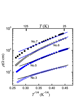
Figure 4 plots the variation of log with for four representative ZnO films, as indicated. The symbols are the experimental data and the straight solid lines are the least-squares fits to the Eq. (3) given below. Clearly, in every sample, there exists a linear regime from 80 K down to 25 K. This observation suggests that, in this interval, the dominate electrical conduction process is due to the Mott VRH conduction mechanism in three dimensions: Mott79
| (3) |
where is a temperature insensitive resistivity parameter, and = is a characteristic temperature. is the electronic density of states at the Fermi level, and is the localization length of the relevant electronic wave function. The average hopping distance and the average hopping energy of the conduction electrons are, respectively, given by = and =. Gantmakher05 Our extracted values of , and then calculated values of , , and are listed in Table III. In order to calculate these three quantities, we have used 2 nm, the Bohr radius of the shallow donors in ZnO. McCluskey09 Our fitted values are significantly smaller than our film thickness (1 m). Also, the criterion 1 for Eq. (3) to be valid is satisfied in the films Nos. 3 and 5–7. On the other hand, this criterion is not satisfied for the films Nos. 2 and 4, because these two films are not resistive enough to lie sufficiently deep on the insulating side of the metal-insulator transition. Huang10 Furthermore, our extracted values of (40 K)1–4 meV are somewhat smaller than the corresponding values reported in Ref. Huang10, . This small decrease in by 35% from that in Ref. Huang10, can be readily understood as arising from the increased shallow donor concentrations in these films as a result of thermal cycling/annealing. Obviously, on average, a higher donor concentration will lead to a lower thermal activation energy involved in the VRH conduction process.
Our observation of the Mott VRH conduction in the interval 20–80 K in this work demonstrates that this carrier transport process in the ZnO material is generic and robust, while the values of the relevant parameters may differ somewhat from run to run, because the amounts of donor concentration could have varied. At even lower measurement temperatures (20 K), a crossover from the Mott VRH conduction process to the Efros-Shklovskii VRH conduction process ES84 should be expected, as has previously been reported in Ref. Huang10, . Unfortunately, the base temperature of our closed-cycle refrigerator does not allow measurements down to sufficiently low to illustrate this latter VRH conduction mechanism in the present work.
III.2.3 Estimate of shallow donor concentration
While the shallow donor concentration, , in the ZnO material is a very important quantity, it is difficult to measure directly. However, we may estimate this quantity from the extracted value which characterizes the -conduction channel in Eqs. (1) and (2). At sufficiently high temperatures (in practice, above a few hundreds K), the shallow donors should have essentially all been ionized. These excited electrons would move in the conduction band and be in response to an externally applied electric field. The resulted electrical conductivity from this -conduction channel can approximately be expressed by ==, where is the electron elastic mean free time, is the effective electron mass, and is the electron mobility. Typically, the value of in ZnO at above a few hundreds K can be extrapolated to a magnitude of 10 cm2/V s. Ellmer08 In the case of our as-grown single crystal, Table I lists a value 1 cm. Then, we may estimate = cm-3. In the case of our polycrystalline films, Table II lists a value 1 cm. Then, we may estimate = cm-3. These inferred shallow donor concentrations in the single crystal and in the polycrystalline films, respectively, are in good accord with the accepted corresponding values reported in the literature. Look03 ; Ellmer08 This degree of agreement provides a self-consistency check of our data analyses and the interpretation of the charge transport processes in ZnO in this section.
IV Conclusion and Summary
We have investigated the electrical conduction properties of ZnO single crystal and polycrystalline films in the wide temperature range 20–500 K. In the case of single crystal, we found that two types of thermal activation conduction processes dominate the carrier transport at 110 K. As a result, a group of shallow donors and a group of intermediately deep donors, together with their individual ionization energies, have been inferred. In particular, we observed that the shallow donor concentration is markedly affected by thermal cycling in vacuum, strongly suggesting the important role of oxygen vacancies as shallow donors in the ZnO material. In the case of oxygen deficient polycrystalline films, additional conduction processes due to the nearest-neighbor-hopping conduction and the Mott variable-range-hopping conduction mechanisms are observed. These two additional conduction possesses originate from the existence of far more numerous amounts of shallow donors (oxygen vacancies) in polycrystal films, which led to the formation of a partially filled impurity band. Taken together with our previous work (Ref. Huang10, ), this present study provides a fairly complete picture of the overall electrical conduction processes in the ZnO materials.
A summary of the overall electrical conduction processes in the ZnO materials: We would like to give a brief summary of the rich electrical conduction processes in the intensively studied, scientifically and technologically alluring ZnO materials. As the temperature progressively increases from liquid-hilum temperatures up to 500 K, one expects to see, one process by one process, (1) the Efros-Shklovskii variable-range hopping conduction, (2) the Mott variable-range hopping conduction, (3) the nearest-neighbor-hopping conduction, (4) the thermal activation conduction from the shallow donor levels, and finally (5) the thermal activation conduction from the intermediately deep donors levels. The conduction processes (1)–(3) take place in the shallow donor impurity band, while the conduction processes (4) and (5) take place in the conduction band. These conduction mechanisms are generic and robust in unintentionally doped n-type ZnO materials which lie on the insulating side of the metal-insulator transition. split However, the temperature interval within which each conduction mechanism is found and the extracted value of the associated parameter may vary more or less from experiment to experiment. Such variations can readily arise from the fact that different experiments usually involve differing amounts of donors and differing donor level distributions in the samples.
Acknowledgements.
The authors are grateful to S. P. Chiu for experimental assistance and valuable discussion. This work was supported by the Taiwan National Science Council through Grant No. NSC 99-2120-M-009-001 and the MOE ATU Program (J.J.L.), and by the Key Project of Chinese Ministry of Education through Grant No. 109042 and NSF of Tianjin City through Grant No. 10JCYBJC02400 (Z.Q.L.).References
- (1) A. Janotti and C. G Van de Walle, Rep. Prog. Phys. 72, 126501 (2009).
- (2) M. D. McCluskey and S. J. Jokela, J. Appl. Phys. 106, 071101 (2009).
- (3) Ü. Özgür, Y. I. Alivov, C. Liu, A. Teke, M. A. Reshchikov, S. Doǧan, V. Avrutin, S.-J. Cho, and H. Morkoc, J. Appl. Phys. 98, 041301 (2005).
- (4) K. Ellmer, in Transparent Conductive Zinc Oxide, edited by K. Ellmer, A. Klein, and B. Rech (Springer, New York, 2008), Chap. 2.
- (5) Z. Q. Li, D. X. Zhang, and J. J. Lin, J. Appl. Phys. 99, 124906 (2006).
- (6) D. C. Look, Mater. Sci. Eng. B 80, 383 (2001).
- (7) R. Kumar and N. Khare, Thin Solid Films 516, 1302 (2008).
- (8) A. Tiwari, C. Jin, J. Narayan, and M. Park, J. Appl. Phys. 96, 3827 (2004).
- (9) S. P. Heluani, G. Braunstein, M. Villafuerte, G. Simonelli, and S. Duhalde, Thin Solid Films 515, 2379 (2006).
- (10) T. Tsurumi, S. Nishizawa, N. Ohashi, and T. Ohgaki, Jpn. J. Appl. Phys., Part 1 38, 3682 (1999).
- (11) Y. L. Huang, S. P. Chiu, Z. X. Zhu, Z. Q. Li, and J. J. Lin, J. Appl. Phys. 107, 063715 (2010).
- (12) Y. Zhang, G. Du, X. Yang, B. Zhao, Y. Ma, T. Yang, H. C. Ong, D. Liu, and S. Yang, Semicond. Sci. Technol. 19, 755 (2004).
- (13) MTI Corporation, 860 South 19th Street, Richmond, CA 94804, USA.
- (14) H. von Wenckstern, M. Brandt, H. Schmidt, G. Biehne, R. Pickenhain, H. Hochmuth, M. Lorenz, and M. Grundmann, Appl. Phys. A 88, 135 (2007).
- (15) R. Schifano, E. V. Monakhov, B. G. Svensson, W. Mtangi, P. Janse van Rensburg, and F. D. Auret, Physica B 404, 4344 (2009).
- (16) S. P. Chiu, Y. H. Lin, and J. J. Lin, Nanotechnology 20, 015203 (2009).
- (17) L. T. Tsai, S. P. Chiu, J. G. Lu, and J. J. Lin, Nanotechnology 21, 145202 (2010).
- (18) Well below room temperatures, the closed-cycle refrigerator served as a cryopump. The diffusion pump was therefore disconnected to prevent a backflow of its oil vapor into the refrigerator.
- (19) The intermediately deep donor concentration should be much higher than the shallow donor concentration. This can be seen from the fact that, once is sufficiently high and the intermediately deep donors are excited, the -conduction channel dominates the sample conductance. Notice that in Table 1 the values are 5 to 6 orders of magnitude lower than the corresponding values. An estimate of the shallow donor concentration is given in subsection IIIB.3.
- (20) Strictly speaking, the values are sightly reduced from 29 to 25–26 meV after repeated thermal cycling. This can be ascribed to a slight increase in the donor concentration and thus an associated weak dispersion of the shallow impurity levels.
- (21) A Janotti and C. G. Van de Walle, Appl. Phys. Lett. 87, 122102 (2005).
- (22) L. S. Vlasenko and G. D. Watkins, Phys. Rev. B 71, 125210 (2005).
- (23) S. B. Zhang, S.-H. Wei, and A. Zunger, Phys. Rev. B 63, 075205 (2001).
- (24) S. Lany and A. Zunger, Phys. Rev. B 72, 035215 (2005).
- (25) N. F. Mott and E. A. Davis, Electronic Processes in Non-Crystalline Materials, 2nd ed. (Clarendon, Oxford, 1979).
- (26) D. C. Look, C. Coskun, B. Claflin, and G. C. Farlow, Physica B 340–342, 32 (2003).
- (27) H. Tampo, A. Yamada, P. Fons, H. Shibata, K. Matsubara, K. Iwata, S. Niki, K. Nakahara, and H. Takasu, Appl. Phys. Lett. 84, 4412 (2004).
- (28) In case the grain boundary in a polycrystalline semiconductor film forms a depletion region, the thermionic emission effect on the electrical conduction might need to be taken into consideration. See, for example, Refs. Heluani06, and Tsurumi99, . In this study, our films are single-phased and possess a good -axis texture (Ref. Huang10, ), and thus the grain boundary effect does not play a notable role.
- (29) V. F. Gantmakher, Electrons and Disorder in Solids, (Clarendon, Oxford, 2005).
- (30) B. I. Shklovskii and A. L. Efros, Electronic Properties of Doped Semiconductors (Springer, New York, 1984).
- (31) If a sample lies sufficiently close to the metal-insulator transition, the “split-impurity-band” conduction process may take place, as has recently been observed in relatively heavily and natively doped, single-crystalline ZnO nanowires (Refs. Chiu09, and Tsai10, ). In this case, the shallow impurity band splits into a lower subband and an upper subband as a consequence of the presence of excessive randomness and strong Coulomb interactions, see Refs. Mott79, and ES84, .