Optical study of the multiple charge density wave transitions in ErTe3
Abstract
We present an optical spectroscopy study on singe crystalline ErTe3, a rare-earth-element tri-telluride which experiences two successive charge density wave (CDW) transitions at Tc1 = 267 K and Tc2 = 150 K. Two corresponding gap features, centered at 2770 cm-1 ( 343 meV) and 890 cm-1 ( 110 meV) respectively, are clearly seen in ordered state. A pronounced Drude component, which exists at all measurement temperatures, demonstrates the partial gap character of both CDW orders. About half of the unmodulated Fermi surface (FS) remains in the CDW state at the lowest measurement temperature. The study also reveals that fluctuation effect is still prominent in this two-dimensional (2D) material.
pacs:
71.45.Lr, 78.20.-e, 78.30.ErI Introduction
Charge density waves (CDWs), as typical broken symmetry states in solids,densitywave have received considerable attention in the past decades. To date, the CDW orders are accepted to be predominantly driven by the nesting of the metallic Fermi surfaces (FSs). Such nesting would cause a divergence of the electronic susceptibility and response function at the nesting wave vector kF, resulting in instability of the FS. An energy gap in the single particle excitation spectrum would open near the Fermi level, leading to lowering of the total energy of the system. In real space, the instability would result in a spatially periodical modulation of charge density distribution with a period of = . Mediated by the electron-phonon coupling, it also causes a displacement or superstructure distortion of the underlying lattice. Up to now, a great deal of experimental and theoretical investigations have been done aiming at exploring and understanding the intriguing collective quantum phenomena in a variety of CDW materials. The low dimensional systems, which have a highly anisotropic crystal structures, are especially concerned due to the relatively easy realization of the FS nesting condition. Nevertheless, except for the one-dimensional electron system, perfect nestings among the entire FS could hardly be achieved in real materials. More often, only parts of the FS are nested, which could be connected by a wave vector that matches with a peculiar phonon anomaly. In this circumstance, only partial energy gap opens on the FS in the optimally nested area and some metallic channels are saved in ordered state.
The discovery of the CDW character in the rare-earth tri-telluride RTe3 (R=Y, La, and rare earth elements) systems TEMCDW has provided an ideal opportunity to probe the CDW properties, which have been well characterized by the FS nesting driven mechanism. theory ; SmTe3 ; ARPESCeTe3400meV ; ARPESCeTe3 ; ARPESRTe3 ; ARPES2CDW RTe3 has a layered, weakly orthorhombic crystal structure (No. 63 space group Cmcm), structure ; structure2 making up of two nearly square Te nets, which are separated by an insulating corrugated RTe slab. The former undertakes the metallic conductive task while the latter plays a role of charge reservoirs. structure2 ; ARPESCeTe3400meV The lattice of the compounds have an incommensurate modulation with a wave vector of approximately 2/7c∗ in the CDW state. TEMCDW The transition temperature decreases monotonically on traversing the lanthanides series from lighter rare-earth to heavier ones, material ; quenchCDW ; 2CDW which is slightly below the room temperature for the heavy rare-earth RTe3 2CDW but believed to be even above the melting point for the first several light rare-earth compounds.SmTe3 ARPES study has well demonstrated the evolution of the CDW properties, ARPESRTe3 including the effect of chemical pressure on the energy gaps and the distribution of the order parameter in reciprocal space. Meanwhile, in consistent with the rather high transition temperatures, the energy gap scale has been reported to have an order of several hundred meV. SmTe3 ; ARPESCeTe3400meV ; ARPESCeTe3 ; RTe3che.pres ; ARPESRTe3 ; opticalCeTe3
Recently, apart from the above mentioned higher transitions, another anomaly was observed in the transport measurement 2CDW of the heavy rare-earth RTe3 (R = Dy, Ho, Er, Tm) materials, which reveals that there exists another transition at a lower temperature. Then the notion is further confirmed by the following X-ray diffraction study. 2CDW A group of superlattice peaks, which develop below the transition, indicate that it has a CDW origin. The study reflects that a lattice modulation, which holds a wave vector along a∗ axis, occurs perpendicular to the first one. Subsequent ARPES investigation of ErTe3, ARPES2CDW one of the heavy rare-earth tri-telluride which has two well separated transitions at 267 K and 155 K, observed multiple gap features at 10 K, which strengthened the notion that multiple CDW orders coexist in the system. The unmodulated spectral weight, which locates in the neighborhood of c∗ axis in reciprocal space, was largely removed from the FS due to the first CDW gap formation, which is consistent with the previous ARPES studies on light rare-earth tri-telluride. Furthermore, the intensity on the original FS in the vicinity of a∗ axis is also clearly reduced, and then it is ascribed to the development of the second CDW order. The two energy gaps revealed by ARPES measurement are = 175 meV and = 50 meV, respectively. ARPES2CDW
Optical spectroscopy is a powerful bulk sensitive technique to detect the energy gaps in ordered state and yields a great wealth of information in CDW systems. The recent report of optical study on ErTe3 opticsHoEr suggests a partial gap formation roughly at 3000 cm-1 at low temperatures. Although the compound experiences two well separated CDW transitions, 2CDW which are both believed to locate at rather high energy scales, ARPES2CDW no information responsible for the second CDW transition was found in earlier optical measurement. Here we present an optical study on single crystalline ErTe3. In sharp contrast to the previous assertion, the temperature dependent spectra clearly reflect the development and evolution of both CDW orders. The first CDW transition has an energy gap 2 = 2770 cm-1 ( 343 meV) and the second one 2 = 890 cm-1 ( 110 meV) in the CDW state, both being in good agreement with the ARPES measurement.
II EXPERIMENT AND RESULTS
The as-grown single crystalline samples of ErTe3, on which all the present measurements performed, were grown by a self-flux method which was illustrated in detail in our earlier work. opticalCeTe3 The plate-like single crystal with shining golden surface (about 44 mm2) is flexible and much convenient to cleave. We noticed that the sample is much more air- and moisture-sensitive than the light rare-earth element RTe3 compounds. opticalCeTe3 After an exposure in air just a few days, the samples became soft and frail associated with a progressively darker surface. In order to avoid the deterioration, we have tried our best to diminish the samples' exposure time in air. Once the growth process came to the end and the single crystal was obtained, we carried out the measurements as soon as possible. Before each measurement process, the newly cleaved fresh surface is obtained. Meanwhile, each measurement was carried out several times to guarantee the repeatability and identity of the experimental results.
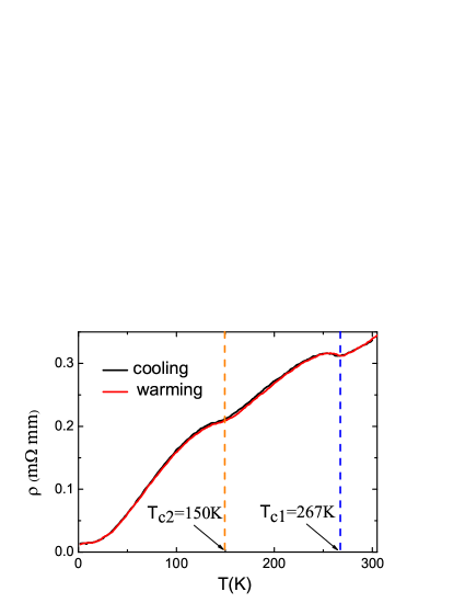
The temperature dependence of the in-plane (ac-plane) dc conductivity is obtained by the standard four-probe method and plotted in figure 1. In consistent with previous studies, 2CDW two obvious anomalies near Tc1 = 267 K and Tc2 = 150 K exhibit in the curve which are ascribed to the two CDW transitions. No clear hysteresis is observed between cooling and warming process which is a clue that both transitions are second-order like. 2CDW ; ARPES2CDW The overall metallic behavior reveals that the FS is only partially affected across the two CDW transitions. ARPES2CDW
The optical reflectivity measurement was bought out on a combination of Bruker IFS 113v and 80v/s spectrometers in a frequency range from 40 to 40000 cm-1. An in situ gold and aluminium overcoating technique was used to get the reflectivity R(). Kramers-Kronig transformation of R() is employed to get the real part of the conductivity spectra . A Hagen-Rubens relation was used for the low frequency extrapolation. In accordance with our earlier work, opticalCeTe3 a constant value of high frequency extrapolation was used up to 100000 cm-1 , above which an relation was employed.
The main panel of figure 2 focuses on the low frequency range of the optical reflectivity spectra R() up to 5000 cm-1 , while its inset displays the expanded range up to 36000 cm-1 at two selected temperatures. The most significant character in R() spectra is the development of a strong dip feature located in the mid-infrared region upon cooling. We notice that there already exists a board suppression near 1500 cm-1 in the room temperature spectrum. During cooling precess, the dip feature, which has been rather obvious at 200 K, becomes more and more dramatic. At the lowest temperature it is rather pronounced. Furthermore, the center of the depletion shows a notable shift towards higher energies, roughly at 2500 cm-1 at 10 K. Additionally, at a lower energy scale a second apparent suppression near 900 cm-1 is observed in R() at 10 K. In opposition to the first one, it is much less pronounced and could not be clearly identified at the measurement temperatures above 100 K. It is worthy noting that the suppressions are typical features of FS gap formation caused by density wave instabilities. opticalCeTe3 ; opticalTaS2 ; opticalBaFe2As2 ; opticalNaFeAs As we shall elaborate below, these are the behaviors in reflectance corresponding with the two CDW orders respectively.
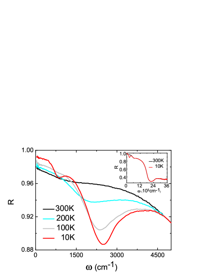
From the inset of figure 2, it could be concluded that all the spectra at varied temperatures coincide together roughly at 4700 cm-1 , above which, the reflectance decreases slowly overall at first and displays an obvious broad kink near 6700 cm-1 . Different from the above mentioned two suppressions, the kink is already present at room temperature and exhibits no temperature dependence. As discussed in the next section, it should be ascribed to the inter-band transition. As frequency continues to proceed, the spectra drop sharply and form a well-defined reflectance edge (plasma edge), then merge with the background reflectance contributed from the inter-band transitions. The well-defined plasma edge, together with the rather high reflectivity in the extremely low frequency region, demonstrate that the compound is a good metal even if it enters the CDW state. Below the two CDW energy scales, the reflectance increases monotonically when lowing temperatures, which is consistent with the dc resistivity measurement. It reinforces the metallic character of the material down to low temperatures, thus the FS is only partially gapped associated with the development of the CDW orders.
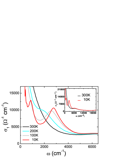
The real part of conductivity is displayed in figure 3 with its inset providing a global description in full range. A pronounced Drude component exists at all temperatures, confirming the metallic behaviors. While in the CDW state, a notable mid-infrared peak near 2800 cm-1 emerges in at 10 K. As temperature increases, the peak shifts slightly to lower energies and decreases in magnitude, tends to vanish at room temperature spectra eventually. Furthermore, another similar peak feature at a lower energy scale appears only at 10 K. Corresponding with the two dip characters in R(), both peak features in indicate the CDW gap properties. Additionally, we note that the inter-band transition peak near 6700 cm-1 is also clearly seen at all temperatures.
III DISCUSSION
300K 47 1.00 – – – – – – 6.7 5.0 24 200K 41 0.55 – – – 2.0 2.1 28 6.7 4.8 23 100K 39 0.41 – – – 2.6 2.1 31 6.7 4.7 23 10K 32 0.15 0.89 0.65 19 2.8 1.7 31 6.7 4.6 23
To analyze the evolution of both the itinerant carrier resonance and the CDW gap excitations in a quantitative way, the spectra are fitted by the Drude-Lorentz model in the whole frequency range for all four temperatures:
| (1) |
Here, is the dielectric constant at high energy, the middle and last terms are the Drude and Lorentz components, respectively. A Drude term is employed to reproduce the metallic response and a selection of Lorentz components are used for the finite frequency excitations, including the double peak gap features below the transition temperatures, an evident near-infrared peak centered roughly at 6700 cm-1 , and two high energy ingredients above 25000 cm-1 for inter-band transitions. The fit results at 10 K are presented in the main panel of figure 4 with its inset revealing the room temperature counterpart. In addition, the temperature dependence of the fit parameters, apart from the two high energy constant inter-band transitions, are listed in table 1. In sharp contrast to the other terms of which the parameters experience remarkable changes at varied temperatures, the parameters of the third Lorentz component almost exhibit no temperature dependence. The central peak position is roughly pinned at 6700 cm-1 ( 830 meV). The charge excitation locates at such a high energy scale that it most likely originates from the inter-band transitions. In the following part the discussions will be focused on the plasma frequencies, Drude scattering rates and the two CDW gaps.
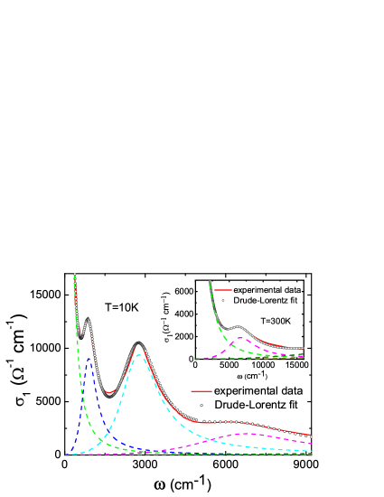
It is well known that the free carrier resonance governs the Drude component behaviors. The Drude spectral weight determines the plasma frequency , the square of which is proportional to the effective carrier density n/m∗ (where m∗ is the effective carrier mass). In addition, the width of the Drude peak is just the scattering rate = 1/ (where is the average life time of free carriers). The plasma frequency = 47100 cm-1 at 300 K reduces to 32000 cm-1 at 10 K. Provided that the effective mass of free carriers remains the same at different temperatures, the area of the FS at 10 K will be 46% of that at room temperature, meaning that about half of the FS is gapped away from EF. For the sake of verification and comparison, another approach is adopted to estimate the ungapped fraction of the FS: opticsHoEr
| (2) |
Where is the plasma frequency, is the mode strength of the ith Lorentz peak. The calculation gives a value = 44 at 10 K. The above conclusion is well evidenced by the nearly same value.
Unlike the relatively moderate change of the plasma frequency, the scattering rate experiences much stronger variations. The room temperature value = 1025 cm-1 drops to 150 cm-1 at 10 K, namely which reduces by about 85. It seems that the openings of partial CDW gaps remove the electrons near Fermi level which undergo stronger scattering. opticalCeTe3 Associated with the loss of scattering channels, the metallic behavior reveals an enhancement of the dc conductivity down to low temperatures.
Now the emphasis is assigned to the discussion of the CDW properties. At the lowest temperature, spectra develop two typical gap features, the first one centered at 2770 cm-1 ( 343 meV) and the second 890 cm-1 ( 110 meV). It should be mentioned that the electrodynamics of density wave ground states have been well established and understood. Due to the first case coherence factor in the electrodynamic response, optical conductivity in density wave state shows a sharp maximum at the gap frequency. opticalBaFe2As2 ; Degiorgi At finite temperatures, the thermally excited electrons contribute a low frequency tail. Therefore, the double peak features can be identified as the corresponding CDW behaviors in optical spectroscopy. Meanwhile, the peak positions indicate the two CDW gaps. Combined with the transition temperatures, we can get the ratio 2/ kBTCDW = 14.9 for the first CDW order and 8.5 for the second one. Both ratios are much higher than the weak coupling theory predictions. It is worthy pointing out that both CDW gap values obtained from the optical spectroscopy measurement match well with that extracted from ARPES experiments, ARPES2CDW where a larger gap = 175 meV and a smaller one = 50 meV are obtained. Double of both values are almost identical with our results. Thus the present optical study is in good agreement with the ARPES measurement. In the previous optical report on the same compound, opticsHoEr only one gap feature near 3000 cm-1 was found. As we have mentioned above, the material is air- and moisture-sensitive. The surface degradation, if exposing in air for a bit longer time, may cause the discrepancy.
The evolution of the gap properties is apparent at varied temperatures. During warming process, in spectra the larger gap peak exhibits a sizable shift towards lower energies and decreases in magnitude, becomes invisible at room temperature at last. On the other hand, the corresponding suppression in R(), as mentioned above, is clearly present at 300 K. It is most likely that the weak character due to Lorentz excitation in the room temperature spectra is covered by the high frequency tail of the large Drude component. opticsHoEr They match so well that we could not distinguish the charge excitation across the CDW gap from the itinerant carrier response. However, the transition temperature Tc1 = 267 K in dc conductivity is well below the room temperature. The fact that CDW characters emerge above the transition supports the notion in this two-dimensional compound fluctuation effect is still prominent. Such effect is also confirmed by the observation in X-ray diffraction experiment 2CDW of superlattice peaks with broadened width well above Tc1. In addition, although the second transition temperature Tc2 = 150 K is well above 100 K, the corresponding CDW gap excitation which exists in at 10 K could not be identified at 100 K. In contrast to the pronounced peak feature of the first CDW gap, the peak magnitude corresponding with the second CDW order is much weaker. Meanwhile, the peak position centered at 890 cm-1 is very close to the giant zero energy excitations. So we believe that the disappearance of the second CDW peak in at 100 K has the same reason with the invisibility of the first one at 300 K.
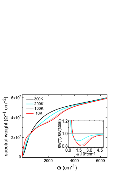
To gain more insight into the band structure variation accompanied with the CDW gap formations, a spectral weight analysis is present. The spectral weight as a function of frequency is plotted in figure 5 with the normalized one showing in the inset. In the extremely low frequency range, in consistent with the overall metallic behavior observed in dc resistivity measurement, the spectral weight increases monotonically with decreasing temperatures, due to the narrowing and rising of the Drude component. In the mid-infrared frequency range roughly between 700 cm-1 and 4500 cm-1 , the spectral weight at lower temperatures becomes smaller than that at higher ones. The redistribution clearly indicates the CDW gap formation. The inset of figure 5 shows that a notable minimum emerges in the normalized spectral weight in this area. At 10 K a minimal value 82% reaches at 2000 cm-1 . Consisting with the movement of the peak position in , shifts remarkably to low frequency with increasing temperatures, indicating that the CDW gaps tend to close. Above the spectral weight differences between different temperatures diminish gradually, suggesting a spectral weight transfer from the low frequency region below to high frequency area above . Roughly above 9000 cm-1 the curves for different temperatures merge together, indicating that the spectral weight is fully recovered. In the whole frequency range the curve at 300 K is rather smooth, while subtle characters exist in the spectra at 10 K. There appears a slight downturn centered at 700 cm-1 , manifesting the opening of the smaller CDW gap. Additionally, another much striking suppression, verifying the formation of the larger gap, occurs in a broad frequency range from 1500 cm-1 to 3500 cm-1 .
It should be noted that, in contrast to the first CDW transition observed in the rare-earth based RTe3 compounds, material which is pronounced to exist almost in the whole lanthanides series, 2CDW the second CDW order is only reported in a fraction of the RTe3 materials. 2CDW ; opticalCeTe3 Apart from the prior reports of the second CDW transition brought out by transport 2CDW and ARPES measurement, ARPES2CDW the present work undoubtedly confirmed the coexistence of multiple CDW transitions in ErTe3, one of the heavy rare-earth tri-telluride. Our earlier study on CeTe3 opticalCeTe3 has provided an optical evidence that multiple CDW orders also exist in the light rare-earth tri-telluride. Therefore, it is natural to ask whether or not the presence of the multiple CDW orders is a common feature in the rare-earth based RTe3 compounds. Then, more systematic experimental investigations on various rare-earth based RTe3 compounds would be necessary.
IV CONCLUSIONS
To conclude, we have performed an optical investigation on the two CDW phase transitions of ErTe3. The well-defined plasma frequency edge, which exhibits in the whole temperature scope, and the rather high reflectivity in low frequency range both demonstrate the well-behaved metallicity even in the CDW state. The depletion features in R() and corresponding peak characters in both clearly reflect the development of the two CDW orders upon cooling. Two energy gaps 2 = 343 meV and 2 = 110 meV at 10 K are obtained via the Drude-Lorentz fit procedure. As the Drude component never disappears at low temperatures, the FS in the ordered state is only partially gapped. An optical estimation suggests that about half of the original FS is gapped away. The broad suppression feature in R() at room temperature, which is yet above the first CDW transition, reflects that fluctuation effect also plays an important role in this 2D material.
ACKNOWLEDGMENTS
This work was supported by the National Science Foundation of China (10834013, 11074291), and the 973 project of the Ministry of Science and Technology of China (2011CB921701).
References
- (1) G. Grüner, Density Waves in Solids (Addison-Wesley, Reading, MA, 1994).
- (2) E. DiMasi, M. C. Aronson, J. F. Mansfield, B. Foran, and S. Lee, Phys. Rev. B 52, 14516 (1995).
- (3) J. Laverock, S. B. Dugdale, Zs. Major, M. A. Alam, N. Ru, I. R. Fisher, G. Santi, and E. Bruno, Phys. Rev. B 71, 085114 (2005).
- (4) G. H. Gweon, J. D. Denlinger, J. A. Clack, J. W. Allen, C. G. Olson, E. D. DiMasi, M. C. Aronson, B. Foran, and S. Lee, Phys. Rev. Lett. 81, 886 (1998).
- (5) V. Brouet, W. L. Yang, X. J. Zhou, Z. Hussain, N. Ru, K.Y. Shin, I. R. Fisher, and Z. X. Shen, Phys. Rev. Lett. 93, 126405 (2004).
- (6) H. Komoda, T. Sato, S. Souma, T. Takahashi, Y. Ito, and K. Suzuki, Phys. Rev. B 70, 195101 (2004).
- (7) V. Brouet, W. L. Yang, X. J. Zhou, Z. Hussain, R. G. Moore, R. He, D. H. Lu, Z. X. Shen, J. Laverock, S. B. Dugdale, N. Ru, and I. R. Fisher, Phys. Rev. B 77, 235104 (2008).
- (8) R. G. Moore, V. Brouet, R. He, D. H. Lu, N. Ru, J. H. Chu, I. R. Fisher, and Z. X. Shen, Phys. Rev. B 81, 073102 (2010).
- (9) B. K. Norling and H. Steinfink, Inorg. Chem. 5, 1488 (1966).
- (10) E. DiMasi, B. Foran, M. C. Aronson, and S. Lee, Chem. Mater. 6, 1867 (1994).
- (11) N. Ru, C. L. Condron, G. Y. Margulis, K. Y. Shin, J. Laverock, S. B. Dugdale, M. F. Toney, and I. R. Fisher, Phys. Rev. B 77, 035114 (2008).
- (12) A. Sacchetti, C. L. Condron, S. N. Gvasaliya, F. Pfuner, M. Lavagnini, M. Baldini, M. F. Toney, M. Merlini, M. Hanfland, J. Mesot, J. H. Chu, I. R. Fisher, P. Postorino, and L. Degiorgi, Phys. Rev. B 79, 201101(R) (2009).
- (13) N. Ru and I. R. Fisher, Phys. Rev. B 73, 033101 (2006).
- (14) A. Sacchetti, L. Degiorgi, T. Giamarchi, N. Ru, and I. R. Fisher, Phys. Rev. B 74, 125115 (2006).
- (15) B. F. Hu, P. Zheng, R. H. Yuan, T. Dong, B. Cheng, Z. G. Chen, and N. L. Wang, Phys. Rev. B 83, 155113 (2011).
- (16) F. Pfuner, P. Lerch, J. H. Chu, H. H. Kuo, I. R. Fisher, and L. Degiorgi, Phys. Rev. B 81, 195110 (2010).
- (17) W. Z. Hu, G. Li, J. Yan, H. H. Wen, G. Wu, X. H. Chen, and N. L. Wang, Phys. Rev. B 76, 045103 (2007).
- (18) W. Z. Hu, J. Dong, G. Li, Z. Li, P. Zheng, G. F. Chen, J. L. Luo, and N. L. Wang, Phys. Rev. Lett. 101, 257005 (2008).
- (19) W. Z. Hu, G. Li, P. Zheng, G. F. Chen, J. L. Luo, and N. L. Wang, Phys. Rev. B 80, 100507(R) (2009).
- (20) L. Degiorgi, M. Dressel, A. Schwartz, B. Alavi, and G. Grüner, Phys. Rev. Lett. 76, 3838 (1996).