Persistence of Topological Order and Formation of Quantum Well States in Topological Insulators Bi2(Se,Te)3 under Ambient Conditions
The topological insulators represent a unique state of matter where the bulk is insulating with an energy gap while the surface is metallic with a Dirac cone protected by the time reversal symmetryTin3D ; ZhangQiPT ; HasanKaneRev ; ZhangQiRMP ; JMoorePer . These characteristics provide a venue to explore novel quantum phenomena in fundamental physicsXLQiNP ; RDLiAxions ; XLQiMomo ; LFuMajorana ; RYuSience and show potential applications in spintronics and quantum computingRevnextgeneration ; ZhangQiPT ; JMoorePer . One critical issue directly related with the applications as well as the fundamental studies is how the topological surface state will behave under ambient conditions (1 atmosphere air and room temperature). In this paper, we report high resolution angle-resolved photoemission measurements on the surface state of the prototypical topological insulators, Bi2Se3, Bi2Te3 and Bi2(Se0.4Te2.6), upon exposing to ambient conditions. We find that the topological order persists even when the surface is exposed to air at room temperature. However, the surface state is strongly modified after such an exposure. Particularly, we have observed the formation of two-dimensional quantum well states near the surface of the topological insulators after the exposure which depends sensitively on the original composition, x, in Bi2(Se3-xTex). These rich information are crucial in utilizing the surface state and in probing its physical properties under ambient conditions.
The angle-resolved photoemission spectroscopy (ARPES) is a powerful experimental tool to directly identify and characterize topological insulatorsHasanARPES . A number of three-dimensional topological insulators have been theoretically predicted and experimentally identified by ARPESBiSbARPES ; BiSeTheo ; Bi2Se3ARPES ; Bi2Te3ARPES ; TlBiSe2Theo ; TlBiSe2ARPES ; some of their peculiar properties have been revealed by scanning tunneling microscopy (STM)TZhangSTM ; YazdaniSTM ; KaptulnikSTM ; PCheng ; Hanaguri . The application of the topological surface states depends on the surface engineering that can be manipulated by incorporation of non-magneticLAWraypn ; mnmi ; ccvb ; crs or magneticYLChenFe ; ZHasanPertur ; LAWraypn ; mnmi impurities or gas adsorptionsZHasanPertur ; LPlucinski ; LAWraypn ; HMBenia . While the ARPES and STM measurements usually involve the fresh surface obtained by cleaving samples in situ under ultra-high vacuum, for the transport measurements which are widely used to investigate the intrinsic quantum behaviors of the topological surface stateDXQu ; JGAnalytis ; ZRen ; JChen , and particularly the ultimate utilizations of the topological insulators, the surface may be exposed to ambient conditions (1 atmosphere air and room temperature) or some gas protection environment. It is therefore crucial to investigate whether the topological order can survive under the ambient conditions, and furthermore, whether and how the surface state may be modified after such exposures.
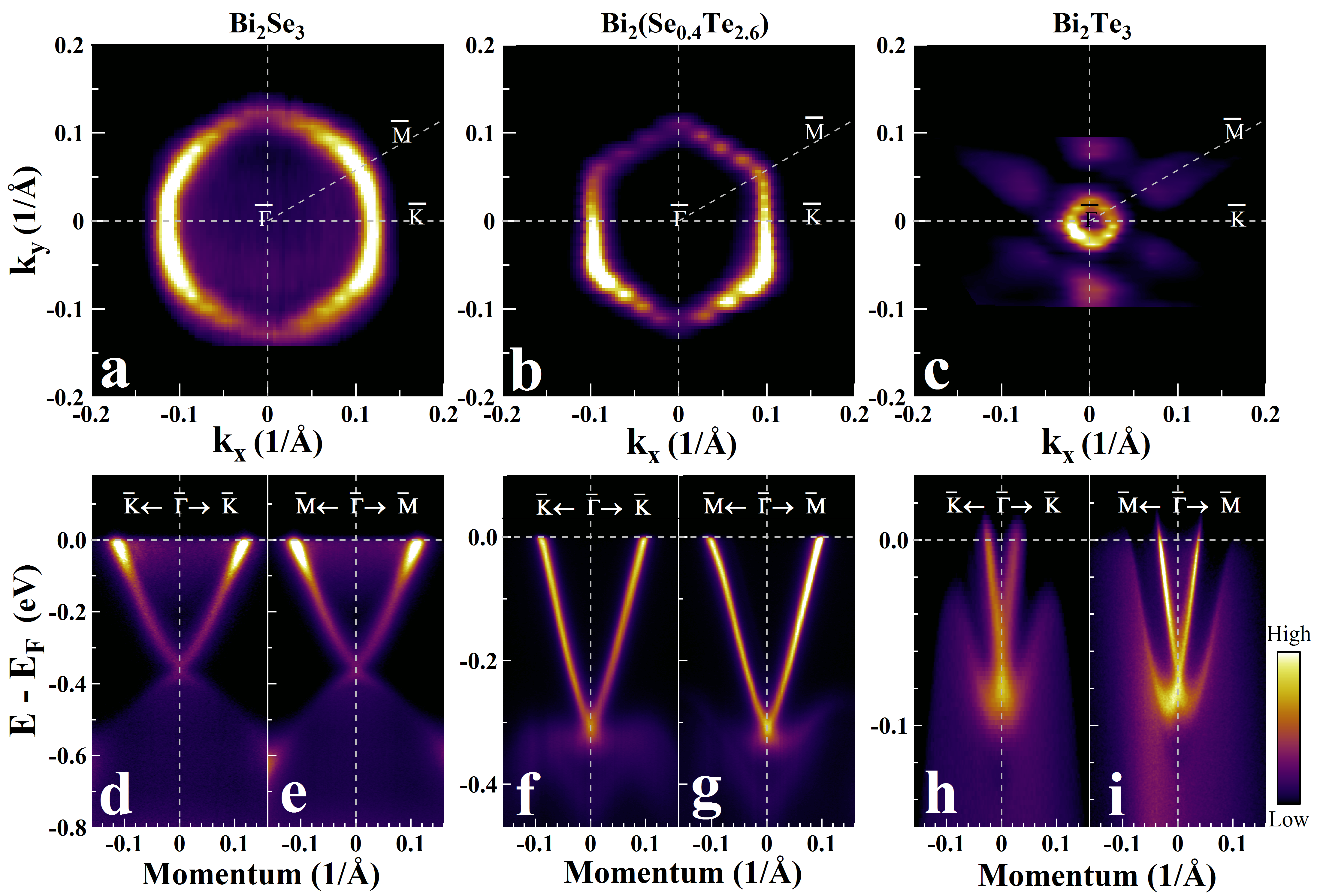
We start by first looking at the electronic structure of the prototypical topological insulators Bi2(Se,Te)3 under ultra-high vacuum. The Fermi surface and the band structure of the Bi2(Se3-xTex) topological insulators depend sensitively on the composition, x, as shown in Fig. 1. The single crystal samples here were all cleaved in situ and measured at 30 K in an ultra-high vacuum (UHV) chamber with a base pressure better than 5 10-11 Torr. For Bi2Se3, a clear Dirac cone appears near -0.36 eV (Figs. 1d and 1e); the corresponding Fermi surface (Fig. 1a) is nearly circular but with a clear hexagon-shape in the measured dataHexBi2Se3 . It is apparently of n-type because the Fermi level intersects with the bulk conduction band. On the other hand, the Dirac cone of the Bi2Te3 sample lies near -0.08 eV (Figs. 1h and 1i), much closer to the Fermi level than that reported before (-0.34 eV in Bi2Te3ARPES ). The corresponding Fermi surface (Fig. 1c) becomes rather small, accompanied by the appearance of six petal-like bulk Fermi surface sheets. These results indicate that our Bi2Te3 sample is of p-type because the Fermi level intersects the bulk valence band along the - direction. This is also consistent with the positive Hall coefficient measured on the same Bi2Te3 sampleCZhang . This difference of the Fermi surface topology and the location of the Dirac cone from othersBi2Te3ARPES may be attributed to the different carrier concentration in Bi2Te3 due to different sample preparation conditions. In our Bi2(Se3-xTex) samples, we have seen a crossover from n-type Bi2Se3 to p-type Bi2Te3. In order to eliminate the interference of the bulk bands on the surface state near the Fermi level, we fine tuned the composition x in Bi2(Se3-xTex) and found that, for x=2.6, nearly no spectral weight can be discerned from the bulk conduction band, as seen from both the Fermi surface (Fig. 1b) and the band structure (Figs. 1f and 1g). A slight substitution of Te by Se in Bi2(Se0.4Te2.6) causes a dramatic drop of the Dirac point to -0.31 eV (Figs. 1f and 1g) and an obvious hexagon-shaped Fermi surface (Fig. 1b). It is interesting to note that the hexagon-shape of Bi2(Se0.4Te2.6) (Fig. 1b) is rather pronounced, although its Fermi surface size is smaller than that of Bi2Se3 (Fig. 1a). The hexagonally-shaped Fermi surface observed in the topological surface states reflects the hybridization of surface electronic states with the bulk states and can be theoretically explained by considering the higher order terms in the k p HamiltonianHexWarp .
In order to directly examine how the topological surface state behaves under ambient conditions in the topological insulators, we carried out our ARPES measurements in different ways. (1). We first cleaved the sample in situ and performed ARPES measurement in the ultra-high vacuum (UHV) chamber. The sample was then pulled out to another chamber filled with 1 atmosphere N2 gas, exposed for about 5 minutes, before transferring back to the UHV chamber to do ARPES measurements; (2). We cleaved and measured the sample in the UHV chamber, and then pulled the sample out to air for 5 minutes before transferring back to the UHV chamber for the ARPES measurements; (3). We cleaved the sample in air and then transferred it to the UHV chamber to do the ARPES measurement. Our measurements show that the above procedures of exposure to air or N2 produce similar and reproducible results for a given sample.
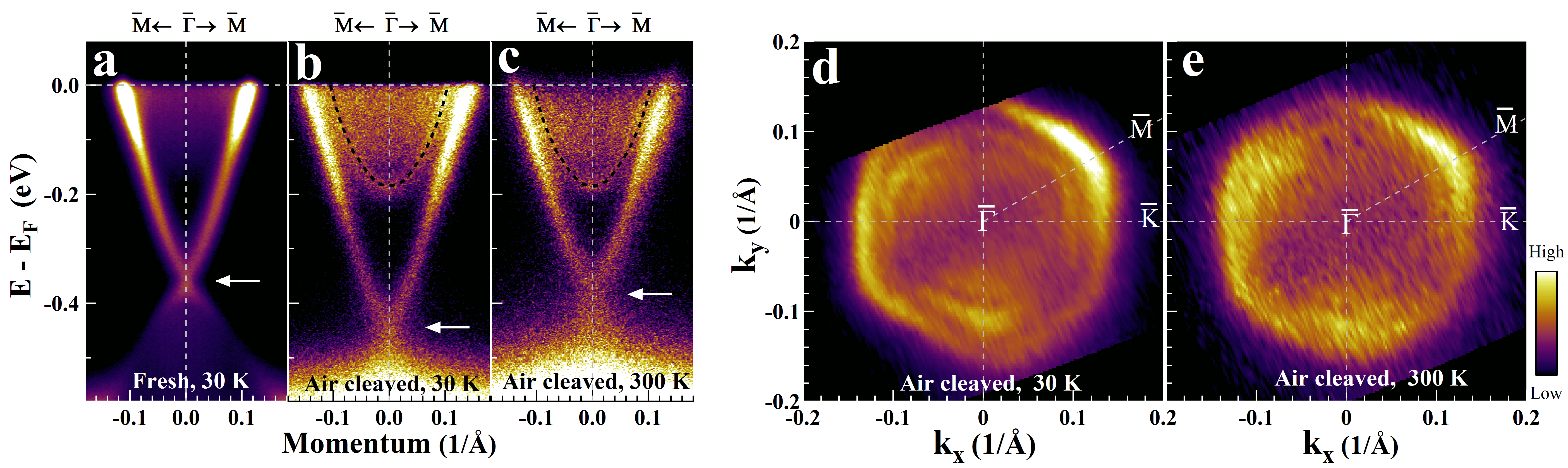
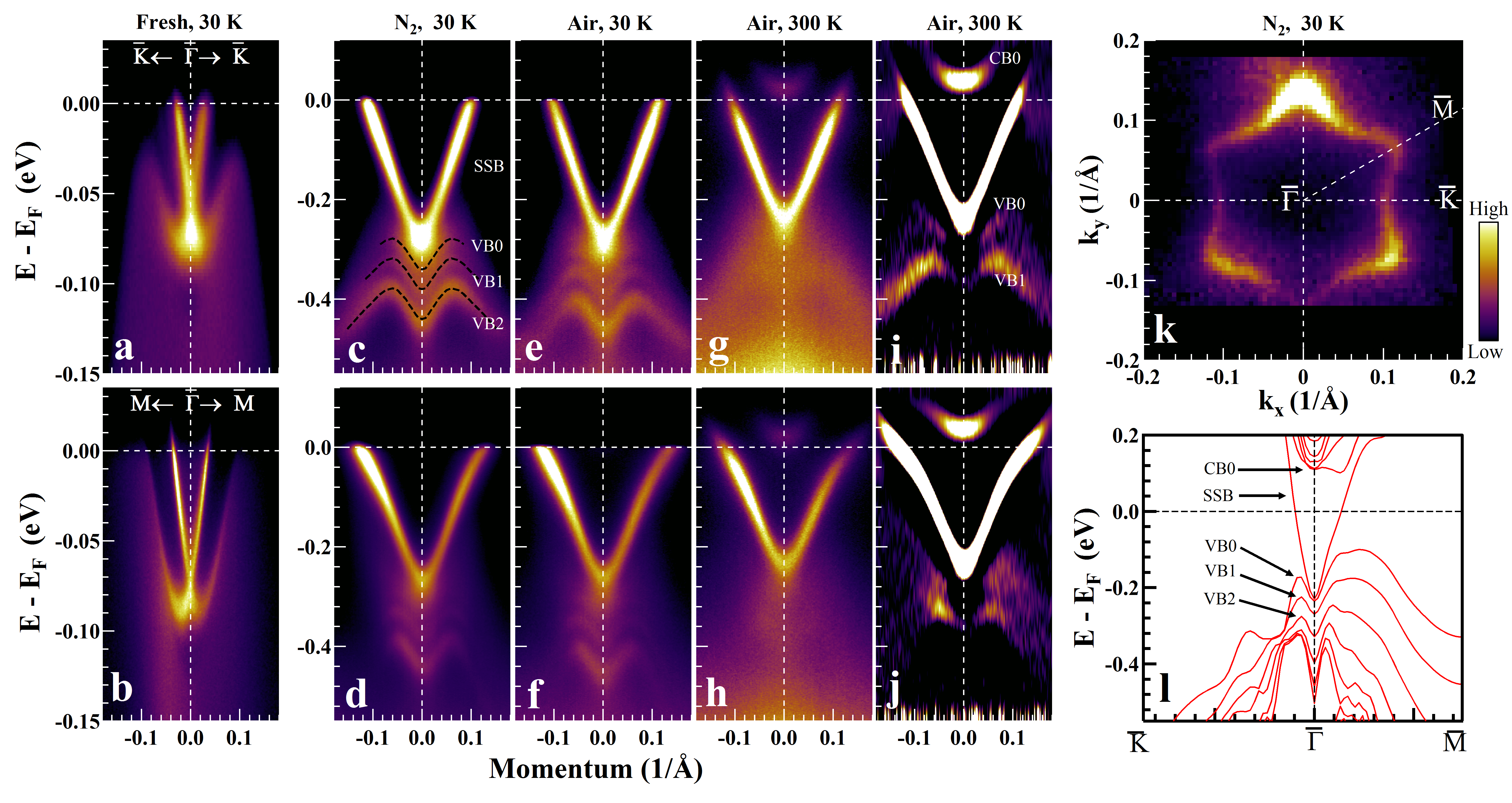
The surface exposure of the topological insulators to air or N2 gives rise to a dramatic alteration of the surface state, as shown in Figs. 2, 3 and 4, for Bi2Se3, Bi2(Se0.4Te2.6), and Bi2Te3, respectively, when compared with those for the fresh surface (Fig. 1). The first obvious change is the shifting of the Dirac cone position relative to the Fermi level. For Bi2Se3, Bi2(Se0.4Te2.6) and Bi2Te3, it shifts from the original -0.36 eV (Figs. 1d and 1e), -0.31 eV (Figs. 1f and 1g), -0.08 eV (Figs. 1h and 1i) for the fresh surface to -0.48 eV (Fig. 2b), -0.40 eV (Figs. 3a and 3b), and -0.28 eV [Figs. 4(c-f)] at 30 K for the exposed surface, respectively. In all these cases, the shift of the Dirac cone to a larger binding energy indicates an additional doping of electrons into the surface state. The exposure also gives rise to a dramatic change of the surface Fermi surface. For Bi2Se3, in addition to a slight Fermi surface size increase, an obvious change occurs in the Fermi surface shape that the hexagon-shape becomes much more pronounced in the exposed surface (Fig. 2d) than that in the fresh sample (Fig. 1a). For Bi2(Se0.4Te2.6), one clearly observes the much-enhanced warping effect in the exposed surface (Fig. 3c) when compared with the nearly standard hexagon in the fresh surface (Fig. 1b). The most dramatic change occurs for Bi2Te3 where not only the Fermi surface size increases significantly, but also the warping effect in the exposed surface (Fig. 4i) becomes much stronger. Overall, the exposure causes the lowering of the Dirac cone position, an increase of the surface Fermi surface size, and an obvious enhancement of the Fermi surface warping effect in the Bi2(Se3-xTex) system.
The topological order in the Bi2(Se3-xTex) topological insulators is robust even when the surface is exposed to ambient conditions, in spite of all the alterations mentioned above. One clearly observes the persistence of the Dirac cone in the exposed surface as in Bi2Se3 (Figs. 2b and 2c), in Bi2(Se0.4Te2.6) (Figs. 3a and 3b), and Bi2Te3 (Figs. 4(c-h)). Particularly, this is the case for the surface exposed to air and measured at room temperature (Fig. 2c for Bi2Se3, and Figs. 4g and 4h for Bi2Te3). On the other hand, after the exposure, although the signal of the surface state gets weaker for Bi2Se3 (Fig. 2), it remains rather strong for Bi2(Se0.4Te2.6) (Fig. 3) and Bi2Te3 (Fig. 4). This is in a stark contrast to the conventional trivial surface state where minor surface contamination will cause the extinction of the surface stateHuefner . The robustness of the topological order to Coulomb, magnetic and disorder perturbations has been reported beforeZHasanPertur ; LPlucinski . Our present observations directly demonstrate the robustness of the topological order against absorption and thermal process under ambient conditions due to the protection of the time-reversal symmetryHasanKaneRev ; ZhangQiRMP .
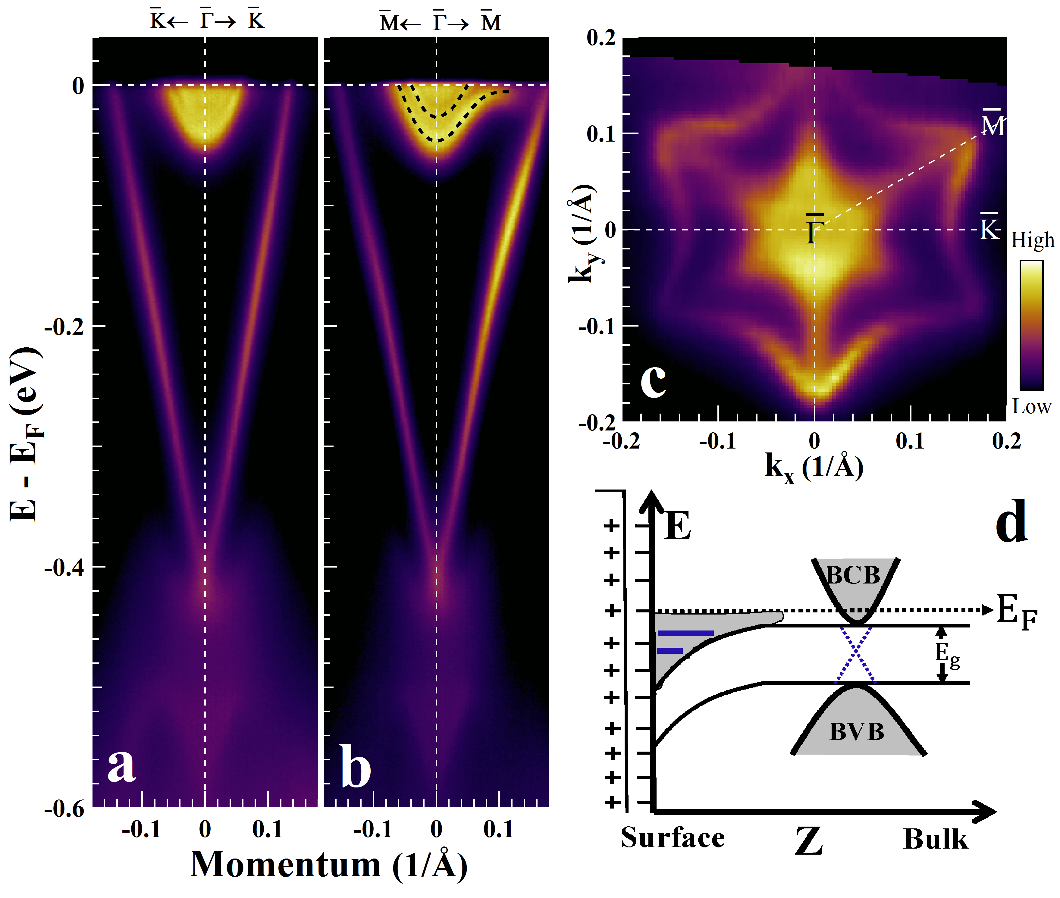
The surface exposure to air or N2 in the Bi2(Se3-xTex) topological insulators produces two-dimensional electronic states near the surface. In Bi2Se3, the exposure gives rise to additional parabolic bands, as schematically marked by the dashed line in Figs. 2b and 2c. Correspondingly, this leads to additional Fermi surface sheet(s) inside the regular topological surface state (Figs. 2d and 2e). In Bi2(Se0.4Te2.6), this effect gets more pronounced and the newly emerged bulk conduction band splits into several discrete bands, as marked by the dashed lines in Fig. 3b. While the band quantization effect occurs in the bulk conduction band in Bi2(Se0.4Te2.6), it shows up in the valence band in the exposed Bi2Te3 surface, as shown in Figs. 4(c-h), where one can see a couple of discrete “M”-shaped bands. The quantized bands are obvious at low temperature and get slightly smeared out when the temperature rises to room temperature (Figs. 4g and 4h).
The formation of the split bands in the exposed surface of the topological insulators is reminiscent of the quantum well states observed in the quantum confined systemsSiAg and in some topological insulatorstdeg ; mnmi ; crs ; ccvb ; HMBenia ; KingReshba . There are a couple of possibilities that the quantum well states may be formed. One usual way is due to band bending effect. As mentioned before, the surface exposure to air or N2 causes an electron transfer to the surface of the topological insulators. The accumulation of these additional electrons near the surface would lead to a downward bending of the bulk bands near the surface region, as schematically shown in Fig. 3d, resulting in a “V”-shaped potential well where the bulk conduction band of electrons can be confined. This picture, as proposed beforetdeg ; ccvb , seems to be able to explain the two-dimensional quantum well states in the conduction bands in Bi2(Se0.4Te2.6) (Figs. 3a and 3b). However, it becomes questionable to explain the quantum well states observed in the bulk valence band of Bi2Te3 (Figs. 4c-j). In this case, the downward band bending no longer acts as a quantum well potential for the valence band top because the charge carriers are hole-like. The band-bending is therefore not a general picture that can explain the formation of the two-dimensional quantum well states in Bi2(Se0.4Te2.6) (Figs. 3a and 3b) and Bi2Te3 (Fig. 4) topological insulators on the same footing. An alternative scenario is the expansion of van der Waals spacings in between the quintuple layers (QLs) caused by the intercalation of gasesSVEremeev . The observation of multiple split bands with different spacings would ask for multiple van der Waals gaps with different expansions. Whether and how these can be realized in the exposed surface remains to be investigated. We note that our observations of multiple split bands are similar to those seen in the ultra-thin films of Bi2Se3YZhang and Bi2Te3YYLi . From our first principle band structure calculations on Bi2Te3 with different number of quintuple layers, we also find that a detached slab with a thickness of 7 quintuple layers can give a rather consistent description (Fig. 4l) of our observed results in terms of the quantitative spacings between the 3 resolved bands (VB0, VB1, and VB2 bands as marked in Figs. 4c and 4l). In addition, the distance between the conduction band bottom (CB0 band in Figs. 4i and 4l) and the first valence sub-band bottom (VB0 band in Figs. 4i and 4l) is rather consistent between the measured and calculated results. These seem to suggest that a “confined surface slab” with nearly 7 quintuple layers may be formed after the exposure that acts more or less independently from the bulk. More work needs to be done to further investigate whether such a confined surface slab can be thermodynamically stable. Overall, the formation of the two-dimensional quantum well states is a general phenomenon for the exposed surface of the Bi2(Se3-xTex) topological insulators; the effect depends sensitively on the composition x of the samples which may facilitate manipulation of these quantum well states.
The present work has significant implications on the fundamental study and ultimate applications of the topological insulators. Many experimental measurements, such as some transport measurements, involve samples exposed to ambient conditions. The practical applications may involve sample surface either exposed to ambient condition, or be in contact with other magnetic or superconducting materials. On the one hand, the robustness of the topological order under ambient conditions sends a good signal for these experimental characterization and practical utilizations. The formation of the quantum well states may give rise to new phenomena to be studied and utilized. The sensitivity of the surface state to the Bi2(Se3-xTex) composition provides a handle to manipulate these quantum states. On the other hand, the strong modification of the electronic structure and the formation of additional quantum well states in the exposed surface have to be considered seriously in interpreting experimental data and in surface engineering. It is critical to realize before hand that the surface under study or to be utilized may exhibit totally different behaviors as those from the fresh surface cleaved in ultra-high vacuum. In addition to the alteration of electronic states upon exposure, the transport properties of the topological surface state may be further complicated by the formation of quantum well states.
We thank Prof. X. H. Chen for providing us samples at the initial stage of the project, and Prof. Liling Sun and Prof. Zhong-xian Zhao for their help in the characterization of the samples. This work is supported by the NSFC (91021006) and the MOST of China (973 program No: 2011CB921703).
METHODS
Crystal growth methods Single crystals of (x=0, 2.6 and 3) were grown by the self-flux method. Bismuth, selenium and tellurium powders were weighed according to the stoichiometric (x=0, 2.6 and 3) composition. After mixing thoroughly, the powder was placed in alumina crucibles and sealed in a quartz tube under vacuum. The materials were heated to 1000 ∘C, held for 12 hours to obtain a high degree of mixing, and then slowly cooled down to 500 ∘C over 100 hours before cooling to room temperature. Single crystals of several millimeters in size were obtained. The crystal structure of the resulting crystals was examined by use of a rotating anode x-ray diffractometer with Cu Kα radiation ( = 1.5418 Å). The chemical composition of the crystals was analyzed by the energy dispersive X-ray spectroscopy (EDAX) and the induction-coupled plasma atomic emission spectroscopy (ICP-AES). The resistivity of the crystals was measured by the standard four-probe method.
Laser-ARPES methods. The angle-resolved photoemission measurements were carried out on our vacuum ultra-violet (VUV) laser-based angle-resolved photoemission systemLiuARPES . The photon energy of the laser is 6.994 eV with a bandwidth of 0.26 meV. The energy resolution of the electron energy analyzer (Scienta R4000) is set at 1 meV, giving rise to an overall energy resolution of 1 meV which is significantly improved from 1015 meV from regular synchrotron radiation systemsBi2Se3ARPES ; Bi2Te3ARPES . The angular resolution is 0.3∘, corresponding to a momentum resolution 0.004 -1 at the photon energy of 6.994 eV, more than twice improved from 0.009 -1 at a regular photon energy of 21.2 eV for the same angular resolution. Our superior instrumental resolution of laser ARPES has made the measured features of topological insulators in this work much sharper. The Fermi level is referenced by measuring on a clean polycrystalline gold that is electrically connected to the sample. The samples were all measured in vacuum with a base pressure better than 510-11 Torr.
∗Corresponding author: XJZhou@aphy.iphy.ac.cn
References
- (1) Fu, L., Kane, C. L. Mele, E. J. Topological insulators in three dimensions. Phys Rev Lett 98, 106803 (2007).
- (2) Qi, X. L. Zhang, S. C. The quantum spin Hall effect and topological insulators. Physics Today 63, 33-38 (2010).
- (3) Hasan, M. Z. Kane, C. L. Colloquium: Topological insulators. Rev Mod Phys 82, 3045 (2010).
- (4) Qi, X. L. Zhang, S. C. Topological insulators and superconductors. Preprint at http://arxiv.org/abs/1008.2026 (2011).
- (5) Moore, J. E. The birth of topological insulators. Nature 464, 194-198 (2010).
- (6) Qi, X.-L., Hughes, T. L. Zhang, S.-C. Fractional charge and quantized current in the quantum spin Hall state. Nat Phys 4, 273-276 (2008).
- (7) Li, R., Wang, J., Qi, X.-L. Zhang, S.-C. Dynamical axion field in topological magnetic insulators. Nat Phys 6, 284-288 (2010).
- (8) Qi, X.-L., Li, R., Zang, J. Zhang, S.-C. Inducing a magnetic monopole with topological surface states. Science 323, 1184-1187 (2009).
- (9) Fu, L. Kane, C. L. Superconducting proximity effect and Majorana fermions at the surface of a topological insulator. Phys Rev Lett 100, 096407 (2008).
- (10) Yu, R. et al. Quantized anomalous Hall effect in magnetic topological insulators. Science 329, 61-64 (2010).
- (11) Moore, J.E. Topological insulators the next generation. Nat Phys 5, 378-380 (2009).
- (12) Hasan, M. Z. A new experimental approach for the exploration of topological quantum phenomena. Preprint at http://arxiv.org/abs/1105.0396 (2011).
- (13) Hsieh, D. et al. A topological Dirac insulator in a quantum spin Hall phase. Nature 452, 970 (2008).
- (14) Zhang, H. J. et al. Topological insulators in Bi2Se3, Bi2Te3 and Sb2Te3 with a single Dirac cone on the surface. Nat Phys 5, 438 (2009).
- (15) Xia, Y. et al. Observation of a large-gap topological insulator class with a single Dirac cone on the surface. Nat Phys 5, 398 (2009).
- (16) Chen, Y. L. et al. Experimental realization of a three-dimensional topological insulator, Bi2Te3. Science 325, 178 (2009).
- (17) Yan, B. H. et al. Theoretical prediction of topological insulators in thallium-based III-V-VI2 ternary chalcogenides. EPL 90, 37002,(2010); Lin, H. et al. Single-Dirac-cone topological surface states in the TlBiSe2 class of topological semiconductors. Phys Rev Lett 105, 036404 (2010).
- (18) Kuroda, K. et al. Experimental realization of a three-dimensional topological insulator phase in ternary chalcogenide TlBiSe2. Phys Rev Lett 105, 146801 (2010); Sato, T. et al. Direct evidence for the Dirac-cone topological surface states in the ternary chalcogenide TlBiSe2. Phys Rev Lett 105, 136802 (2010); Chen, Y. L. et al. Single Dirac cone topological surface state and unusual thermoelectric property of compounds from a new topological insulator family. Phys Rev Lett 105, 266401 (2010).
- (19) Zhang, T. et al. Experimental demonstration of topological surface states protected by time-reversal symmetry. Phys Rev Lett 103, 266803 (2009).
- (20) Roushan, P. et al. Topological surface states protected from backscattering by chiral spin texture. Nature 460, 1106-1109 (2009).
- (21) Alpichshev, Z. et al. STM imaging of electronic waves on the surface of Bi2Te3: topologically protected surface states and hexagonal warping effects. Phys Rev Lett 104, 016401 (2010).
- (22) Cheng, P. et al. Landau quantization of topological surface states in Bi2Se3. Phys Rev Lett 105, 076801 (2010).
- (23) Hanaguri, T. et al. Momentum-resolved Landau-level spectroscopy of Dirac surface state in Bi2Se3. Phys Rev B 82, 081305(R) (2010).
- (24) Wray, L. A. et al. Electron dynamics in topological insulator semiconductor-metal interfaces (topological p-n interface). Preprint at http://arxiv.org/abs/1102.3935 (2011).
- (25) Bianchi, M. et al. Simultaneous quantization of bulk conduction and valence states through adsorption of nonmagnetic impurities on Bi2Se3. Preprint at http://arxiv.org/abs/1105.3826 (2011).
- (26) Zhu, Z.-H. et al. Rashba spin-splitting control at the surface of the topological insulator Bi2Se3. Preprint at http://arxiv.org/abs/1106.0552 (2011).
- (27) Pan, Z.-H. et al. Scattering on Magnetic and Non-magnetic Impurities on a Surface of a Topological Insulator. Preprint at http://arxiv.org/abs/1104.0966 (2011).
- (28) Chen, Y. L. et al. Massive Dirac Fermion on the surface of a magnetically doped topological insulator. Science 329, 659 (2010).
- (29) Wray, L. A. et al., A topologocal insulator surface under strong Coulomb, magnetic and disorder perturbations, Nature Phys 7, 32 (2011).
- (30) Plucinski, L. et al., Robust surface electronic properties of topological insulators: Bi2Te3 films grown by molecular beam epitaxy. App Phys Lett 98, 222503 (2011).
- (31) Benia, H. M. et al. Reactive chemical doping of the Bi2Se3 topological insulator. Preprint at http://arxiv.org/abs/1105.2664 (2011).
- (32) Qu, D.-X., Hor, Y. S., Xiong, J., Cava, R. J. Ong, N. P. Quantum oscillations and Hall anomaly of surface states in the topological insulator Bi2Te3. Science 329, 821-824 (2010).
- (33) Analytis, J. G. et al. Two-dimensional surface state in the quantum limit of a topological insulator. Nat Phys 6, 960-964, (2010).
- (34) Ren, Z., Taskin, A. A., Sasaki, S., Segawa, K. Ando, Y. Large bulk resistivity and surface quantum oscillations in the topological insulator Bi2Te2Se. Phys Rev B 82, 241306 (2010).
- (35) Chen, J. et al. Gate-voltage control of chemical potential and weak antilocalization in Bi2Se3. Phys Rev Lett 105, 176602 (2010).
- (36) Kuroda, K. et al. Hexagonally deformed Fermi surface of the 3D topological insulator Bi2Se3. Phys Rev Lett 105, 076802 (2010).
- (37) Zhang, C. et al. Phase diagram of a pressure-induced superconducting state and its relation to the Hall coefficient of Bi2Te3 single crystals. Phys Rev B 83, 140504 (2011).
- (38) Fu, L. Hexagonal warping effects in the surface states of the topological insulator Bi2Te3. Phys Rev Lett 103, 266801 (2009).
- (39) Reinert, F. et al. Direct measurements of the L-gap surface states on the (111) face of noble metals by photoelectron spectroscopy. Phys Rev B 63, 115415 (2001).
- (40) Speer, N. J., Tang, S.-J., Miller, T. Chiang, T.-C. Coherent electronic fringe structure in incommensurate silver-silicon quantum wells. Science 314, 1132941 (2006).
- (41) Bianchi, M. et al. Coexistence of the topological state and a two-dimensional electron gas on the surface of Bi2Se3. Nat Commun 1, 128 (2010).
- (42) King, P. D. C. Large tuneable Rashba spin splitting of a two-dimensional electron gas in Bi2Se3. Preprint at http://arxiv.org/abs/1103.3220 (2011).
- (43) Eremeev, S. V. et al. New interpretation of the origin of 2DEG states at the surface of layered topological insulators, Preprint at http://arxiv.org/abs/1107.3208 (2011).
- (44) Zhang, Y. et al., Crossover of the three-dimensional topological insulator Bi2Se3 to the two-dimensional limit, Nat Phys 6, 584 (2010).
- (45) Li, Y. Y. et al., Intrinsic topological insulator Bi2Te3 thin films on Si and their thickness limit. Adv Mater22, 4002 (2010).
- (46) Liu, G. D. et al. Development of a vacuum ultraviolet laser-based angle-resolved photoemission system with a superhigh energy resolution better than 1 meV. Rev Sci Instrum 79, 023105 (2008).