Field-effect modulation of conductance in VO2 nanobeam transistors with HfO2 as the gate dielectric
Abstract
We study field-effect transistors realized from VO2 nanobeams with HfO2 as the gate dielectric. When heated up from low to high temperatures, VO2 undergoes an insulator-to-metal transition. We observe a change in conductance ( 6 percent) of our devices induced by gate voltage when the system is in the insulating phase. The response is reversible and hysteretic, and the area of hysteresis loop becomes larger as the rate of gate sweep is slowed down. A phase lag exists between the response of the conductance and the gate voltage. This indicates the existence of a memory of the system and we discuss its possible origins.
pacs:
71.30.+h,64.70.Nd,73.22.GkVO2 undergoes an insulator-to-metal transition accompanied by a change in its crystal structureeyert ; berglund , the mechanism of which is still under debate. The transition temperature of a free crystal is 341 K. Its proximity to room temperature has motivated attempts at fabricating Mott field-effect transistors (FETs) to induce the phase transition by applying a gate voltage. Such experiments have so far been conducted on thin films of VO2 kim newj ; stefanovich ; vasilev ; ramanathangating . Other interesting applications of VO2 include memory metamaterialsdriscollscience and memristorsdriscollmemristor . Recently it has been realized that single-crystalline VO2 nanobeams support single or ordered metal-insulator domains in the phase transitionjunqiao_first ; cao . This eliminates the random, percolative domain structures occurring in thin films, and allows intrinsic transition physics to be probed. In this letter, we report on electrostatic gating measurements on single crystalline VO2 beams junqiao_first ; cobden using HfO2 as the gate dielectric. The devices have a hysteretic response and appear to possess a memory persisting over a large timescale (a few minutes). The field effect studies have been done at different temperatures in the insulating and metallic phases of the system.

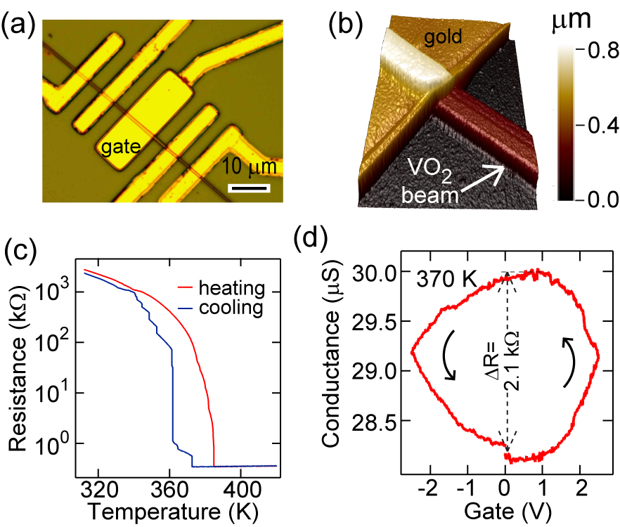
The VO2 beams were grown using the vapor transport techniquejunqiao_first ; supp . Electrodes were designed by electron beam lithography followed by etching in Ar plasma (for removal of organic residue) and sputtering of Cr/Au to make Ohmic contacts. Figs. 1(a) and 1(b) show the optical microscope and atomic force microscope (AFM) images of VO2 devices. The local gate electrode in the middle (Fig. 1(a)) is fabricated by first depositing a 20 nm layer of HfO2 by atomic layer deposition and then sputtering Cr/Au on top. The typical width of the beams is 0.3-1 m, and the thickness is 300-600 nm. Fig. 1(c) shows the resistance of a VO2 beam as a function of temperature (data from Device 1). Stress builds up in the system as it is heated, and the system breaks up into alternating insulator and metal domains cao . The metal domains first appear close to 341 K and on further heating, grow in size and number. The system becomes completely metallic at a much higher temperature. The temperature at which the system turns metallic varies from one device to another (380-400 K), and is dictated by the stress induced due to adhesion to the substrate. (The nanobeams are embedded in a 1.1 m thick layer of SiO2 grown on Si wafers.)
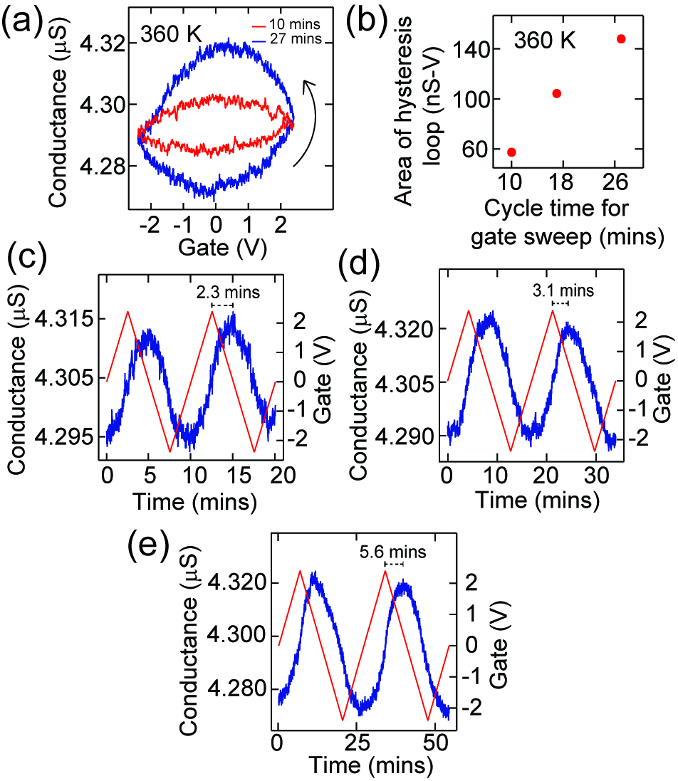
Two and four probe gating experiments were done inside an evacuated variable temperature probe station. Both two and four probe resistances of the same devices were measured (at various temperatures in both the insulating and metallic phases) and found to be similar. This indicates that the contact resistance is negligible compared to the intrinsic resistance of VO2. We have also confirmed that there is no leakage through the gatesupp . Fig. 1(d) shows the effect of gate voltage on the two-probe conductance of a VO2 device (Device 2) at 370 K. The dc gate voltage is swept slowly in a cycle (of duration 20 mins) with limiting values of -2.5 and 2.5 V. (The source-drain current used was set at an ac frequency and monitored with a lock-in amplifier.) Arrows indicate the direction of gate voltage sweep. The response of the conductance is hysteretic. Gate sweeps at different rates were conducted on the devices, with the following observation: the hysteresis loop area and maximum change in conductance become larger on making the rate of gate sweep slower. This is surprising and has been confirmed on several devices.

Fig. 2(a) shows two probe conductance () as a function of gate voltage () at 360 K for Device 3 at different gate voltage sweep-rates. The cycle which is swept slowly over 27 mins (blue curve) has a much larger hysteresis than the one which is swept faster (red curve) in 10 mins. The area of the loop is computed as where the summation extends over one cycle of gate voltage. In Fig. 2(b), it is shown how the area of the loop increases with an increase in the cycle time (i.e., slowing down of the gate voltage sweep-rate). Another intriguing aspect is prominently seen in Figs. 1(d) and 2(a). As we increase up from 0 V to higher positive values (see Fig. 1(d)), increases. At the extreme value of 2.5 V, is reversed backwards. However, does not start reducing immediately. It goes on increasing for a while and starts to reduce only after a time lag. (Denoting time as , we can say that does not change sign simultaneously with .) This implies that the system wants to persist in the state of ‘increasing conductance’ even though the gate voltage has reversed. This is a manifestation of the ‘memory’ or ‘inertia’ of the system. This memory effect diventra is observed at the other extreme of gate voltage (-2.5 V) also. The gate voltage and resulting conductance (data from Device 3) are plotted simultaneously as a function of time in Figs. 2(c)-(e). (Each plot shows two consecutive cycles of gate voltage.) In all these curves, it is seen that the maximum (minimum) of conductance is shifted in time from the maximum (minimum) of gate voltage. This shift, or ‘phase lag’ between the input and output signals, is the signature of a persistent effect. Slower the rate of sweep, larger is the time-delay. It is 5.6 mins for the slowest scan with a 27 mins cycle (Fig. 2(e)).

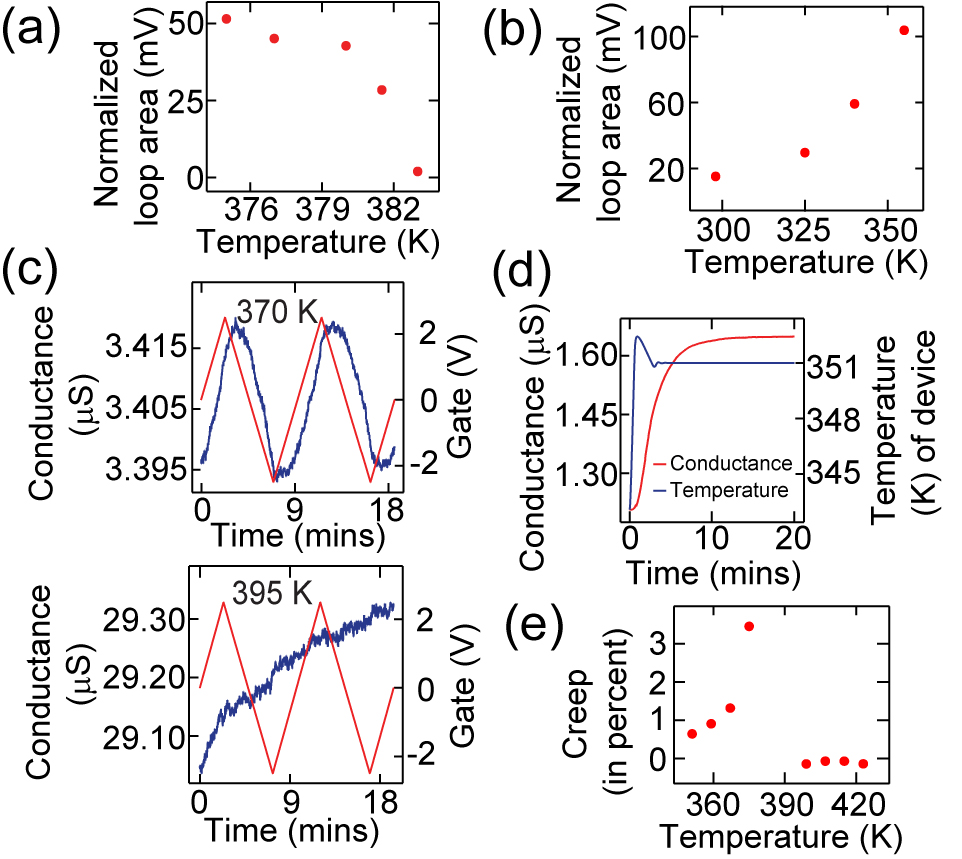
The hysteresis is observed at temperatures at which the beam is in the insulating state, or there is a co-existence of metal and insulator domainsjunqiao_first . No gating is observed in the full metallic state. We compute the ‘normalized loop area’ , where is the conductance at =0. The ‘normalized loop area’ as a function of temperature (close to the metallic transition) for Device 3 is plotted in Fig. 3(a). The most prominent hysteresis for our devices is usually obtained in the temperature range 340-370 K, which is the temperature window in which multiple domains exist along the beamjunqiao_first ; cao . Also, it is shown in Fig. 3(b) how the ‘normalized loop area’ varies over a wide range of temperatures (starting from room temperature) for Device 1.
Fig. 3(c) shows the gate voltage response (as a time chart) for Device 4 at two temperatures. At 370 K, the gate effect ( periodic with ) is observed. At 395 K, the VO2 beam is closer to the full metallic transition and the gate effect has disappeared. However, there is a gradual variation of the conductance with time. This is the phenomenon of thermal ‘creep’ that we see in our devices. The conductance takes a long time to stabilize after the device is heated to a new temperature. This feature is noticed on all our devices and is illustrated in Fig. 3(d) (Device 5). The sample is heated up from 343 K, and it reaches the desired temperature of 351 K within 5 mins. However, even 15 minutes after that, the conductance of VO2 has not stabilized. It goes on increasing at a slow rate. (The fractional change over the last 10 mins is 0.64 percent.) We define a quantity called ‘creep’ as the fractional change in conductance over a period of 10 mins after the sample has reached a new temperature. The variation with temperature of this quantity is plotted in Fig. 3(e). ‘Creep’ becomes quite large just before the metallic transition.
The overall change in is a few percent (6 percent in Fig. 1(d) and 1 percent in Fig. 2(e)). Since the entire length of the wire is not covered by the gate, the fractional change in the gated region of Device 2 (Fig. 1(d)) turns out to be 14.4 percentsupp . The gate voltage primarily affects the carrier density close to the surface within the surface skin layer, the bulk being electrostatically screened from the gate. The threshold carrier concentrationjunqiao cao in VO2 has been estimated to be cm-3. Using this value, it is estimated that the amount of carriers induced by a gate voltage of 2.5 V is 8.3 percent of the intrinsic concentration. This is close (in terms of order of magnitude) to the fractional change in conductance due to gating. Hysteretic gating effects are known to arise in semiconductors due to the presence of surface states at the dielectric interface. These act as trapping centers for electrons. It is generally observed that on slowing down the rate of gate voltage sweep, the system is allowed time to equilibrate and hysteresis reducestrap hysteresis . Hysteresis due to slow traps (with relaxation time of a few minutes) have also been reportedslow traps ; kingston . But, in the aforementioned cases, the observed behavior on varying the sweep rate is the opposite of what we see in our devices. Hence, trap states do not seem to offer a possible explanation in our experiments.
Persistent effects have been observed in earlier studies on VO2 (in two terminal memristive devicesdriscollmemristor and infrared response of gated VO2 filmsqazilbash ). In our experiments, there is no gate leakagesupp and hence, heating can be ruled out as a possible cause behind the persistent effect. There is not much information in literature about mechanical relaxation in VO2. It is probable that mechanical relaxation time in VO2 is quite large. When heated to a new temperature, it would take a considerable period of time for the stress pattern and the relative domain sizes (and hence, conductance) to settle down. This explains the thermal ‘creep’. The VO2 crystal has electric dipoles with antiferroelectric couplingjunqiao cao . The coupling strength will depend upon the spatial separation between the lattice sites, thus providing a coupling between the dipolar arrangement and the strain state. Hence, the gate voltage will also affect the strain state, and relaxation of the dipolar arrangement will have a similar timescale as the mechanical relaxation. This may explain the slow processes leading to the time-delay in gate effects (Figs. 2(c)-(e)).
In summary, we have fabricated three terminal field effect devices from VO2 nanobeams using HfO2 as the dielectric. We observe gate effects in conductance and the response is hysteretic. The dependence of electrostatic gating effects on the sweep rate and a phase lag between the reversal of conductance and gate voltage indicates that our devices have an intrinsic memory with a large timescale of a few minutes. This is interesting from the point of view of probing the physical origin of persistent effect in the insulating phase of VO2. Also, single crystalline nanobeams with a smaller thickness may exhibit more pronounced electrostatic gating effects and can have important implications in the design of Mott FETs and memory devices.
We thank S. Ramanathan and K. L. Narasimhan for discussions. We acknowledge the U. S. Department of Energy Early Career Award DE-0000395 (J. W.) and the Government of India and AOARD-104141 (M. M. D.).
References
- (1) V. Eyert, Ann. Phys. 11, 650 (2002)
- (2) C. N. Berglund and H. J. Guggenheim, Phys. Rev. 185, 1022 (1969)
- (3) H. T. Kim, B. G. Chae, D. H. Youn, S. L. Maeng, G. Kim, K. Y. Kang and Y. S. Lim, New J. Phys. 6, 52 (2004)
- (4) G. Stefanovich, A. Pergament and D. Stefanovich, J. Phys.: Condens. Matter 12, 8837 (2000)
- (5) G. P. Vasil’ev, I. A. Serbinov and L. A. Ryabova, Sov. Tech. Phys. Lett. 3, 139 (1977)
- (6) D. Ruzmetov, G. Gopalakrishnan, C. Ko, V. Narayanamurti and S. Ramanathan, J. Appl. Phys. 107, 114516 (2010)
- (7) T. Driscoll, H. T. Kim, B. G. Chae, B. J. Kim, Y. W. Lee, N. M. Jokerst, S. Palit, D. R. Smith, M. Di Ventra and D. N. Basov, Science 325, 1518 (2009)
- (8) T. Driscoll, H. T. Kim, B. G. Chae, M. Di Ventra and D. N. Basov, Appl. Phys. Lett. 95, 043503 (2009)
- (9) J. Wu, Q. Gu, B. S. Guiton, N. P. de Leon, L. Ouyang and H. Park, Nano Lett. 6, 2313 (2006)
- (10) J. Cao, E. Ertekin, V. Srinivasan, S. Huang, W. Fan, H. Zheng, J. W. L. Yim, D. R. Khanal, D. F. Ogletree, J. C. Grossman and J. Wu, Nat. Nanotechnol. 4, 732 (2009)
- (11) J. Wei, Z. Wang, W. Chen and D. H. Cobden, Nat. Nanotechnol. 4, 420 (2009)
- (12) See Supplemental Material at http://www.tifr.res.in/deshmukh/publications.htm.
- (13) Y. V. Pershin and M. Di Ventra, Adv. Phys. 60, 145 (2011)
- (14) J. Cao, W. Fan, K. Chen, N. Tamura, M. Kunz, V. Eyert and J. Wu, Phys. Rev. B 82, 241101(R) (2010)
- (15) S. A. Dayeh, C. Soci, P. K. L. Yu, E. T. Yu and D. Wang, Appl. Phys. Lett. 90, 162112 (2007)
- (16) T. Hanrath and B. A. Korgel, J. Phys. Chem. B 109, 5518 (2005)
- (17) R. H. Kingston and A. L. McWhorter, Phys. Rev. 103, 534 (1956)
- (18) M. M. Qazilbash, Z. Q. Li, V. Podzorov, M. Brehm, F. Keilmann, B. G. Chae, H. T. Kim and D. N. Basov, Appl. Phys. Lett. 92, 241906 (2008)