Doping of epitaxial graphene on SiC intercalated with hydrogen and its magneto-oscillations
Abstract
We study the charge transfer between a quasi-free-standing monolayer graphene, produced by hydrogen intercalation, and surface acceptor states. We consider two models of acceptor density of states to explain the high hole densities observed in graphene and find the density responsivity to the gate voltage. By studying magneto-oscillations of the carrier density we provide an experimental way to determine the relevant model.
Among numerious ways of graphene fabrication Suspended ; CVD ; BN , one of the promising methods for the top-down manufacturing of electronic devices consists in the graphitization of Si-terminated surface of silicon carbide. Graphene produced by such graphitization resides on an insulating R carbon buffer layer, which is easily spoiled by vacancies and, typically, leads to high graphene doping ChargeBalance . Without special growth protocols, monolayer graphene on Si face of SiC appears to be highly n-doped, with electron density at about cm-2 level QHE1 ; Funct . Also, charged surface donors induce Coulomb scattering, which limits the mobility of electrons in such a material. To improve the transport qualities of graphene and decouple it from the substrate, it has been proposed to use hydrogen intercalation Riedl . Hydrogen breaks Si-C bonds and converts the buffer layer into a quasi-free-standing monolayer graphene (QFMLG), which is usually p-doped Speck due to electron transfer from graphene to acceptor states in the H-terminated surface of SiC.

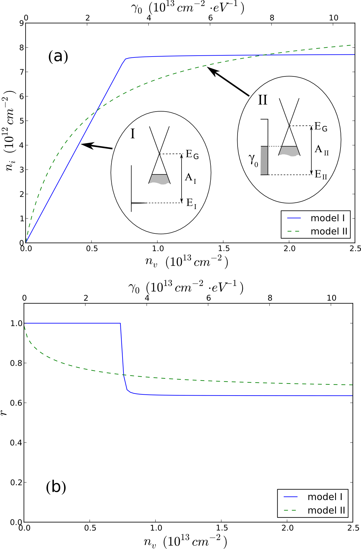
In this work we study the charge transfer between graphene and SiC in hydrogen-intercalated epitaxial graphene, including the magneto-oscillations of the hole density in QFMLG. We consider two limiting models for the charge transfer, which are different by the form of the density of states of surface acceptors, . In the model I we assume that all acceptor states are due to occasional unsaturated Si bonds: vacancies in the hydrogen layer with the density , energy and narrow spectral density , , where is the work function of graphene (Fig. 1, inset I). In the model II we assume a uniform density of states of acceptor levels filled up to the energy (Fig. 1, inset II). For both models we find the hole density in graphene and the responsivity factor describing the effectiveness of QFMLG carrier density control by a gate voltage in a field-effect transistor. We also analyse the oscillations in the carrier density dependence on a magnetic field, and show that this can be used to distinguish experimentally between the two limiting doping models.
The electron transfer from QFMLG to surface acceptor states is described by the following equation,
| (1) |
where is the density of holes in graphene, ( is gate voltage), is the distance between SiC and QFMLG, the Fermi energy (relative to the graphene Dirac point) is , and for the model I and for the model II. Note that integral in Eq. 1 is taken over the electron (rather than hole) energy. Each of the models is characterized by one energy parameter: for model I and for model II.
The value of the carrier density for non-gated structures can be obtained by solving Eq. (1) for . In Fig. 1a we illustrate the hole density dependence in graphene on the amount of acceptors on hydrogenated SiC. For the model I, it is
| (2) |
At a small , all acceptor levels are occupied and . As acceptor density increases, graphene doping saturates at cm-2. Model II also shows a saturation of the carrier density, but with a smoother crossover,
| (3) |

The effectiveness of using QFMLG transistors can be characterized by the responsivity factor, . Then, corresponds to the regime of the effective transistor operation, while indicates that it is difficult to change carrier density in graphene. The responsivity factors for the models I and II,
are compared graphically in Fig. 1b.
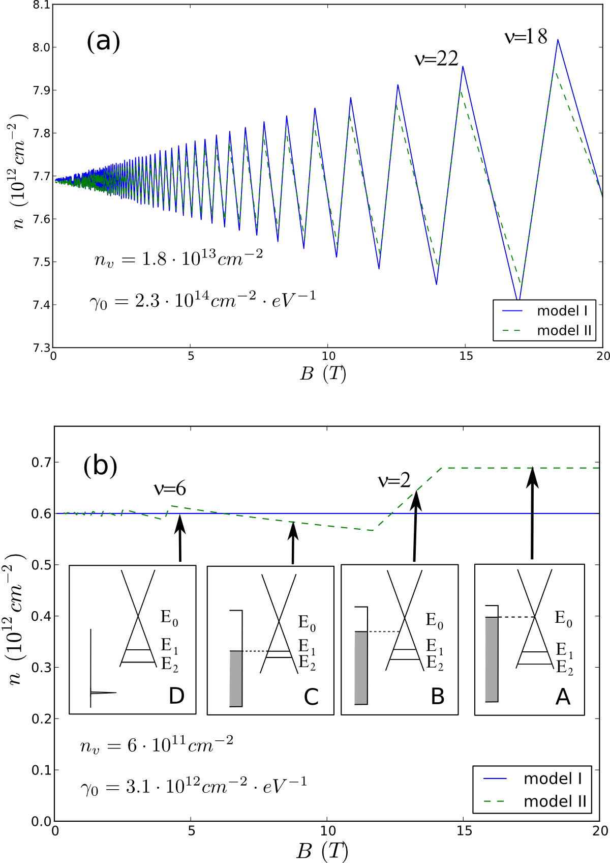
Due to the charge transfer between graphene and acceptors in the hydrogen layer on SiC, carrier density of QFMLG change upon the variation of the magnetic field . For high acceptor densities ( cm-2, cm-2eV-1), Fig. 2a shows the oscillations in dependence, which appear due to a non-zero density of acceptor states at the Fermi level. Similar oscillations were found in graphene on a non-hydrogenated SiC surface QHE , and used to explain the presence of a wide plateau in QHE. Both models give close results for the dependence, which reveals two different regimes. (a) The regions with a negative slope indicating the pinning of the Fermi level to one of the Landau levels in graphene, . To evaluate dependence in this regime we solved Eq. (1), with . (b) The regions with a positive slope corresponding to the pinning of filling factor , for which the Fermi level in the system lies in the acceptor band, between Landau levels.
The difference between the density oscillations in graphene expected on the basis of the models I and II is quite pronounced in structures with low acceptor densities ( cm-2, cm-2eV-1), as shown on Fig. 2b. In this regime no oscillations are observed for model I, in contrast to the model II, where pinning of takes place over magnetic field interval of several Tesla. In the latter case, one can identify the following charge transfer regimes illustrated using sketches in Fig. 2b. At high magnetic fields () the carrier density remains constant, since the 0th Landau level (LL) is partially occupied and the Fermi level in graphene is pinned to the Dirac point (inset A in Fig. 2b). At lower magnetic fields () 0th LL becomes completely unoccupied and the Fermi level sticks to acceptor levels between 0th and 1st LLs (Fig. 2b, inset B). This regime, observed within a window of several T, is responsible for widening the QHE plateau. The region C in Fig. 2b refers to the pinning of the Fermi level to the 1st LL .
In conclusion, we have considered two models of the charge transfer between hydrogen intercalated graphene and acceptors in SiC surface. The first model describes the case when all acceptor states are created by unsaturated Si bonds with energies from a narrow window. The opposite limit of a wide acceptor energy distribution is covered by the second model. Both models predict a saturation behavior of carrier density in graphene as the acceptor density increases, however, the magnetic field dependence of charge transfer in them is very different, especially in structures with a low initial doping cm-2 by holes. As shown in Fig. 2b, the model II features a wide (several T) QHE plateau, while the model I reveals no dependence. One of the ways to detect pinning of filling factor is to measure the activation energy and/or breakdown current of QHE QHE . The width of the peak in the dependence of and breakdown current on the magnetic field in the vicinity of QHE plateau determines the region of filling factor pinning. Alternatively, one can determine the filling factor by looking at the Landau level occupancy using scanning tunneling spectroscopy as in Ref. STS .
References
- (1) Xu Du, I. Skachko, A. Barker, and Eva Y. Andrei, Nature Nanotechnology 3, 491 (2008).
- (2) A. Reina, X. Jia, J. Ho, D. Nezich, H. Son, V. Bulovic, M. S. Dresselhaus, and J. Kong, Nano Lett. 9, 30 (2009).
- (3) W. Gannett, W. Regan, K. Watanabe, T. Taniguchi, M. F. Crommie, and A. Zettl, Appl. Phys. Lett. 98, 242105 (2011).
- (4) S. Kopylov, A. Tzalenchuk, S. Kubatkin, and V. I. Fal’ko, Appl. Phys. Lett. 97, 112109 (2010).
- (5) J. Jobst, D. Waldmann, F. Speck, R. Hirner, D. K. Maude, Th. Seyller, and H. B. Weber, Phys. Rev. B 81, 195434 (2010).
- (6) C. Coletti, C. Riedl, D. S. Lee, B. Krauss, L. Patthey, K. von Klitzing, J. H. Smet, and U. Starke, Phys. Rev. B 81, 235401 (2010͒).
- (7) C. Riedl, C. Coletti, T. Iwasaki, A. A. Zakharov, and U. Starke, Phys. Rev. Lett. 103, 246804 (2009).
- (8) F. Speck, J. Jobst, F. Fromm, M. Ostler, D. Waldmann, M. Hundhausen, H. B. Weber, Th. Seyller, arXiv:1103.3997 (2011).
- (9) T. J. B. M. Janssen, A. Tzalenchuk, R. Yakimova, S. Kubatkin, S. Lara-Avila, S. Kopylov, and V. I. Fal’ko, Phys. Rev. B 83, 233402 (2010).
- (10) Y. J. Song, A. F. Otte, Y. Kuk, Y. Hu, D. B. Torrance, P. N. First, W. A. de Heer, H. Min, S. Adam, M. D. Stiles, A. H. MacDonald, and J. A. Stroscio, Nature 467, 185 (2010).