Controlling the type and density of charge carriers by doping is the key step for developing graphene electronics. However, direct doping of graphene is rather challenge. Based on first-principles calculations, a concept of overcoming doping difficulty in graphene via substrate is reported. We find that doping could be strongly enhanced in epitaxial graphene grown on silicon carbide substrate. Compared to free-standing graphene, the formation energies of the dopants can decrease by as much as 8 eV. The type and density of the charge carriers of epitaxial graphene layer can be effectively manipulated by suitable dopants and surface passivation. More importantly, contrasting to the direct doping of graphene, the charge carriers in epitaxial graphene layer are weakly scattered by dopants due to the spatial separation between dopants and conducting channel. Finally, we show that similar idea can also be used to control magnetic properties, e.g., induces a half-metallic state in the epitaxial graphene without magnetic impurity doping.
Overcoming Doping Difficulty in Graphene via Substrate: A First Principle Study
The conventional silicon based microelectronics is expected to encounter fundamental limitations at nanoscale. According to the semiconductor industry road map, novel materials that could complement or substitute silicon are needed. It is shown that graphene is suitable for coherent nanoscale electronics applications due to its unique electronic properties and extremely high carrier mobilityGeim-2007 ; Castro Neto-2009 ; N. M. R. Peres-2010 . Controlling the type and density of charge carriers by doping is at the heart of graphene electronics. However, the development of reliable chemical doping methods in graphene is still a real challenge. Direct doping of graphene with substitutional dopants is rather difficult, because the strong covalent C-C bonds make graphene as one of the strongest materials in the worldGeim-2007 . Until now, doping of graphene has mainly been achieved through reactive molecular or atomic adsorbates in experimentsT. Ohta-2006 ; S. Y. Zhou-2008 , which is difficult to implement under current device technology. Moreover, direct doping usually suppresses the high carrier mobility of graphene evidentlyGeim-2007 ; Castro Neto-2009 ; N. M. R. Peres-2010 . Thus, new proposals for overcoming the doping difficulty in graphene is urgently needed.
Comparing to mechanical exfoliation of graphene from graphite, large area epitaxial growth of graphene layers on silicon carbide (SiC) surface shows huge application potentials and has apparent technological advantages over the mechanical exfoliation methodC. Berger-2006 ; M. Orlita-2008 . In this letter, we demonstrate that substitutional doping could be strongly enhanced in epitaxial graphene grown on SiC substrate comparing to that of free-standing graphene (FSG). The formation energies of dopants can reduce by as much as 8 eV. The type and density of carriers in epitaxial graphene layer could be effectively manipulated by suitable dopants and surface passivation. Contrasting to direct doping of FSG, the carriers of epitaxial graphene are weakly scattered by dopants due to the spatial separation between scattering centers (dopants) and conducting channel (epitaxial graphene). Thus, the intrinsic high carrier mobility of graphene could be effectively maintained even during doping process. Finally, we show that the same idea also can be used to control spin properties of epitaxial graphene by buffer layer defects. We find that the reconstructed defects in buffer layer can break the spin symmetry of epitaxial graphene and half-metallicity can be induced in the system without magnetic impurity doping.
All the calculations are performed using the method based on density functional theory in the local spin density approximation (LSDA) as implemented in the VASP codeVASP , which is known to describe the structural and electronic properties of graphite quite wellA. Mattausch-2007 ; S. Kim-2008 . The LSDA results are further checked by the generalized gradient approximation and the results are consistent with each other. The electron-ion interaction is described by the projector augmented wave method, and the energy cutoff is set to 400 eV. Structural optimization is carried out on all systems until the residual forces are converged to 0.02 eV/Å. A SiC substrate cell is used to accommodate a 2 2 epitaxial graphene cell, approximating to the larger reconstruction with a periodicity usually observed in experiments. This approximation has been proved to well describe the electronic properties of epitaxial graphene on SiCF. Varchon-2007 ; A. Mattausch-2007 . More importantly, the reconstruction is also been observed in experiments during epitaxial growth of graphene on both (C-terminated) SiC(000) surfaceC. Berger-2006 ; J. Hass-2006 and (Si-terminated) SiC(0001) surfaceForbeaux-1998 ; Rutter-2007 ; Tromp-2009 . To address the doping effects in graphene-SiC system, a SiC substrate cell, which accommodates a 4 4 graphene cell, is constructed. The SiC substrate is modeled by a slab contains 4 SiC bilayers with H passivation on the second surface of the slab. Several test calculations on 6 bilayers and 8 bilayers substates give essentially the same results. A gamma centered 6 6 1 k-point sampling is used for the Brillouin-zone integration, including the Dirac point. In the following, although our discussion is focused on the results of graphene on SiC(000) surface, the results for graphene on SiC(0001) surface will also be mentioned.
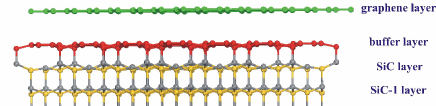
The optimized structure of graphene layers on SiC(000) is shown in Fig. 1. 2/3 of the C atoms in the top SiC surface make covalent bonds with the C atoms of the interface buffer layer (the first graphene layer during vacuum graphitization on SiC), with a C-C bond length 1.62 Å, which drastically changes the Dirac-like band structures of the buffer layer, agreeing with previous resultsF. Varchon-2007 ; A. Mattausch-2007 ; S. Kim-2008 . A similar buffer layer structure is also observed on SiC(0001) surface. The second graphene layer on the top of buffer layer is planar and the distance between the rippled buffer layer and top graphene layer varies between 3.34 - 3.71 Å. The interface buffer layer is stretched by 8% as a result of the lattice mismatch between SiC surface and graphene, agreeing with previous predictionsF. Varchon-2007 ; A. Mattausch-2007 ; S. Kim-2008 .
It is expected that the carriers in graphene could be manipulated by p/n-type dopants, like in conventional semiconductorsA. Franceschetti-1999 . Al, B, P, and N are considered as substitutional dopants, as they are widely used in C- and Si- based materials. All the possible substitutional positions in graphene-SiC system are checked and the formation energies of dopants at different positions are calculated to search the most stable configurations. The formation energy () of a substitutional dopant in graphene-SiC system is defined as:
| (1) |
where and are the total energies of doped and undoped system, respectively. and (dopant = Al, B, P, N) are the chemical potentials of C (or Si) and dopant, respectively. Since epitaxial graphene should grow in C-rich environment, is calculated assuming epitaxial graphene is stable and is calculated so that SiC is stable. It should be noticed that the relative stability between different doping positions does not depend on the particular choice of . The calculated formation energy differences are shown in Fig. 2. Interestingly, Al prefers to substitute Si atom of the SiC substrate or substitute C atom of the interface buffer layer and the of Al decreases dramatically by 8.26 eV compared to FSG case. B and P atoms prefer to substitute C atoms of the buffer layer and the of dopants decrease largely by 2.36 eV and 5.27 eV, respectively, compared to FSG cases. Besides doping in buffer layer, the of B and P at SiC surface are also reduced by 1.46 eV and 4.87 eV, respectively, compared to FSG cases. Contrary to the cases of Al, B, and P doping, N atom prefers to substitute C atom of top SiC substrate with a reduction of by 3.52 eV, as shown in Fig. 2d. The similar phenomenon of substrate-enhanced doping is also found on SiC (0001) surface, with the of dopants decreased by as much as 10.8 eV.
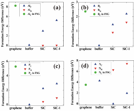
These quite different doping behaviors between different dopants as well as different layers in graphene-SiC system could be understood by considering the structural strain in the various epitaxial graphene-SiC layers, the different atomic covalent radiuses, and the electronegativity of dopants. Since the interface buffer layer is under large tensible strain, Al, B, and P atoms could be easier to substitute C atoms in this layer due to the larger covalent radiuses of Al (1.21 Å), B (0.84 Å), P (1.07 Å) than sp2 C (0.73 Å). The rippled (deformed) structure reduces the doping difficulty in buffer layer to some extent. Furthermore, because the electronegativity of C (2.55) is larger than Si (1.90) in SiC, Si behaves as positively charged cation and C acts as negatively charged anion. Al atom has lower electronegativity (1.61) and a little larger covalent radiuses than Si (1.11 Å), so it would prefer to substitute Si atom in the SiC matrix to increase the negative Coulomb interaction between Al and C. Differing from Al, B, and P, the structural tensile strain increases the difficulty of N doping in the graphene layer because N has a smaller covalent radius (0.71 Å) than C. N atom has even higher electronegativity (3.04) than C, so it would prefer to substitute C atom in the SiC matrix to increase the negative Coulomb interaction between Si and N, which is in agreement with the calculated trend of in Fig. 2d. More importantly, the large reduction of for all the dopants at strain-free SiC substrate (1.46 8.26 eV) indicates that, not only in the structure, the strongly substrate-enhanced doping can also exist in reconstruction because the strain-free substrate is independent of reconstruction in the graphene or buffer layers. The above results and analysis show that overcoming the doping difficulty in graphene could be generally achieved through substrates, and it can also be applied to other layered or thin-film systems. Moreover, it is quite encouraging to see that highly strained graphene (up to 25%) have already been created on substrates in experiments through various schemesK. S. Kim-2009 ; Levy-2010 .
After knowing the stable doping configurations, we turn to investigate how these dopants tune the carrier properties, i.e. carrier type and carrier density, in graphene-SiC system. Without doping, the Dirac-like states in the top epitaxial graphene layer on SiC (000) is preserved, as shown in Fig. 3a. The weakly dispersive interface states visible in Fig. 3a result from the surface dangling bonds of SiC substrate. In our unit cell, there are twelve C sp3 dangling orbitals on the top layer of the SiC substrate. Eight of them make covalent bonds with the buffer layer but the other four remain unsaturated. The localization of C sp3 dangling bonds favor the spin-polarization and thus split to four occupied states and empty states, respectively. Because the band alignment between the epitaxial graphene states and substrate surface states is type-I, therefore, there is no charge transfer between the epitaxial graphene and substrate surface. However, the following results show that the substrate surface states play an important role in affecting the carrier density of top graphene layer.
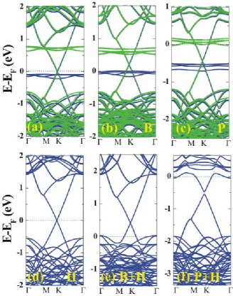
Our total energy calculations indicate that dopants favor to locate at buffer layer or close to buffer layer in the substrate. To understand the carrier distribution, Bader analysisBader is used to estimate the charge variation in the dopant and various layers. We find that after substitutional doping in buffer layer, B atom shows an onsite charge of 1.32 e, whereas in the case of Al doping, the value is substantially lower, 0.80 e. The variation between the Al and B cases could be understood by noticing that B is much more electronegative than Al. When the total hole carrier density is 1.02 1014 cm-2, the hole density in the buffer layer is 5.77 1013 cm-2 after B doping and 9.98 1013 cm-2 after Al doping. Unexpectedly, the top epitaxial graphene is not effectively doped by holes in either cases, with hole density at 5 1012 cm-2. The origin of the small carrier density in the epitaxial graphene layer can be understood from the band structure of the graphene-SiC system. We see that there are localized interface states which strongly pin the Fermi level at about 0.18 eV below the Dirac point for p-type materials, as shown in Fig. 3b. (Al-doping case is similar and not shown here). The hole density of epitaxial graphene is thus limited to 5 1012 cm-2 for p-type doped system. For the n-doped case (Fig. 3c), the empty interface states also play a similar role and pin the Fermi level at about 0.44 eV above the Dirac point, which is responsible to the limited electron density at 1.99 1013 cm-2 in the top epitaxial graphene layer after P doping. The above results strongly demonstrate that although B (Al) and P doping in buffer layer could induce electrons or holes in the top epitaxial graphene, the interface states play as a ”subthreshold valve” to restrict the carrier density. Similar doping behaviors are found when B (Al) and P dope at SiC surface. As we mentioned, N atom prefers to substitute the C atom with dangling bond at the top SiC layer. Contrary to P doping, the epitaxial graphene layer could not be doped with electrons because the N atom is strongly electronegative so the spin-split states of N atom are both occupied after doping.
An obvious route to improve the electron or hole density in epitaxial graphene is by eliminating the influence of the interface states. Since these interface states originate from the dangling orbitals of C atoms at the top of SiC substrate, naturally, we may eliminate them by surface passivation. Here, we take H as an example to demonstrate the surface passivation effect on modulating the charge density of epitaxial graphene. In fact, H intercalation in epitaxial graphene has already been achieved in several experimentsRiedl-2009 ; Guisinger-2009 . The main effect of H adsorption is the disappearance of the interface states, as shown in Fig. 3d. Without these interface states, we expect more electrons or holes will transfer from buffer layer to epitaxial graphene layer. The band structure calculations confirm our idea, as shown in Fig. 3e and 3f for B and P doping, respectively. After surface H passivation, the hole density of B-doped system increases four times up to 2.48 1013 cm-2, which pushes the the Fermi level to 0.42 eV below the Dirac point. Similarly, the electron density of P-doping system increases twice to 3.58 1013 cm-2. Moreover, a small band gap ( 0.07 eV) appears in P-doping system, as shown in Fig. 3f. These results strongly demonstrate that not only we can control the type of carriers in epitaxial graphene via doping of the buffer layer, but also the carrier density could be controlled by substrate passivation. More noticeably, the dopants prefer to stay in the buffer layer while the carriers are concentrated in the top epitaxial graphene. Thus, the carriers in epitaxial graphene layer could be only weakly scattered by dopants due to the spatial separation between scattering centers (dopants) and conducting channel (top graphene layer). This is in the same spirit as in modulation doping in heterostructures such as GaAlAs/GaAsS. Wang-1989 , and we suggest that it is an efficient way in maintaining the high carrier mobility of graphene during doping process.
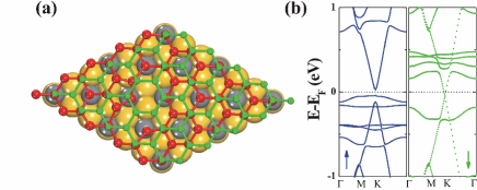
The manipulation of buffer layer not only can be used to control the charge carriers, but also could be used to tune the spins of the system. Here we demonstrate that the reconstructed vacancy in buffer layer has unexpected effect on the spin properties of epitaxial graphene. Injection of high spin-polarized current in graphene is the current subject of intense investigation effortsTombros-2007 . Ideally, 100% spin-polarized current could be induced by half-metallic materials. Although spontaneous vacancy in FSG may induce local spin-polarization, it is rare due to its high formation energy of 8 eV. In graphene-SiC system, we find that vacancy prefers to be formed in buffer layer and undergoes reconstruction, as shown in Fig. 4a. A five-thirteen ring is formed with a of 3.2 eV, which is 5 eV lower than in FSG. The deformed buffer layer as well as the defect reconstruction are responsible for the lower of vacancy in buffer layer. In experiments, considerable amounts of defects have been observed in the interface layer of epitaxial graphene systemRutter-2007 ; Qi-2010 , especially the existence of reconstructed hexagon-pentagon-heptagonQi-2010 . The experimental observations indicate that the of defect in buffer layer is much lower than in FSG, agreeing with our results. It is interesting to see that the reconstructed vacancy not only breaks the honeycomb symmetry, but also breaks the spin symmetry of graphene, which induces a half-metallic state in the top epitaxial graphene layer, as shown in Fig. 4b. There is an apparent gap ( 0.142 eV) in the spin-up state of the epitaxial graphene and a negligible band gap in spin-down state. The localized states near the band edge in spin-up band structure are induced by the C atoms which are bonded to the SiC surface in the five-thirteen ring. It was theoretically predicted that half-metallicity could be induced in graphene by an external electric fieldSon-2006 or transition metal dopingJayasekera-2010 . However, the required electric field is too strong and heavy transition metal elements also often act as poison agents in biological systems. Our results here strongly indicate that SiC-graphene system with reconstructed defects in the buffer layer could have strong potentials for spintronics.
In conclusion, a concept of overcoming doping difficulty in graphene via substrate is reported. We show that substitutional doping could be strongly enhanced in epitaxial graphene on SiC substrate. Compared to free-standing graphene, the formation energies of dopants decrease by as much as 8 eV. The type and density of carriers in epitaxial graphene could be effectively manipulated by suitable dopants and surface passivation. The carriers in epitaxial graphene layer are weakly scattered by dopants due to the spatial separation between the dopants and carriers. Finally, we show that the reconstructed vacancy in buffer layer could induce half-metallicity in epitaxial graphene without magnetic impurity doping. Generally, the effect of substrate-enhanced doping could exist in other substrates, and it can also be applied to other layered or thin-film systems.
The work at NREL was supported by the U.S. Department of Energy under Contract No. DE-AC36-08GO28308. The work at Fudan was partially supported by the National Science Foundation of China.
References
- (1) A. K. Geim and K. S. Novoselov, Nature Mater. 6, 183 (2007).
- (2) A. H. Castro Neto, F. Guinea, N. M. R. Peres, K. S. Novoselov, and A. K. Geim, Rev. Mod. Phys. 81, 109 (2009).
- (3) N. M. R. Peres, Rev. Mod. Phys. 82, 2673 (2010).
- (4) T. Ohta, A. Bostwick, T. Seyller, K. Horn, and E. Rotenberg, Science 313, 951 (2006).
- (5) S. Y. Zhou, D. A. Siegel, A. V. Fedorov, and A. Lanzara, Phys. Rev. Lett. 101, 086402 (2008).
- (6) C. Berger, Z. Song, X. Li, X. Wu, N. Brown, C. Naud, D. Mayou, T. Li, J. Hass, A. N. Marchenkov, E. H. Conrad, P. N. First, and W. A. de Heer, Science 312, 1191 (2006).
- (7) M. Orlita, C. Faugeras, P. Plochocka, P. Neugebauer, G. Martinez, D. K. Maude, A.-L. Barra, M. Sprinkle, C. Berger, W. A. de Heer, and M. Potemski, Phys. Rev. Lett. 101, 267601 (2008).
- (8) G. Kresse and J. Furthmüller, Comput. Mater. Sci. 6, 15 (1996).
- (9) A. Mattausch and O. Pankratov, Phys. Rev. Lett. 99, 076802 (2007).
- (10) S. Kim, J. Ihm, H. J. Choi, and Y. -W. Son, Phys. Rev. Lett. 100, 176802 (2008).
- (11) F. Varchon, R. Feng, J. Hass, X. Li, B. N. Nguyen, C. Naud, P. Mallet, J.-Y. Veuillen, C. Berger, E. H. Conrad, and L. Magaud, Phys. Rev. Lett. 99, 126805 (2007).
- (12) J. Hass, R. Feng, T. Li, X. Li, Z. Zong, W. A. de Heer, P. N. First, E. H. Conrad, C. A. Jeffrey, and C. Berger, Appl. Phys. Lett. 89, 143106 (2006).
- (13) I. Forbeaux, J.-M. Themlin, and J.-M. Debever, Phys. Rev. B 58, 16396 (1998).
- (14) G. M. Rutter, J. N. Crain, N. P. Guisinger, T. Li, P. N. First, J. A. Stroscio, Science 317, 219 (2007).
- (15) R. M. Tromp and J. B. Hannon, Phys. Rev. Lett. 102, 106104 (2009).
- (16) A. Franceschetti and A. Zunger, Nature (London) 402, 60 (1999).
- (17) K. S. Kim et al., Nature (London) 457, 706 (2009).
- (18) N. Levy, S. A. Burke, K. L. Meaker, M. Panlasigui, A. Zettl, F. Guinea, A. H. Castro Neto, M. F. Crommie, Science 329, 544 (2010).
- (19) G. Henkelman, A. Arnaldsson, and H. Jonsson, Comput. Mater. Sci. 36, 354 (2006).
- (20) N. P. Guisinger, G. M. Rutter, J. N. Crain, P. N. First, and J. A. Stroscio, Nano Lett. 9, 1462 (2009).
- (21) C. Riedl, C. Coletti, T. Iwasaki, A. A. Zakharov, and U. Starke, Phys. Rev. Lett. 103, 246804 (2009).
- (22) S. Wang, Fundamentals of Semiconductor Theory and Device Physics (Prentice Hall, London, 1989), Chap. 11, P.542.
- (23) N. Tombros, C. Jozsa, M. Popinciuc, H. T. Jonkman, and B. J. van Wees, Nature (London) 448, 571 (2007).
- (24) Y. Qi, S. H. Rhim, G. F. Sun, M. Weinert, and L. Li, Phys. Rev. Lett. 105, 085502 (2010).
- (25) Y.-W. Son, M. L. Cohen, and S. G. Louie, Nature (London) 444, 347 (2006).
- (26) T. Jayasekera, B. D. Kong, K. W. Kim, and M. B. Nardelli, Phys. Rev. Lett. 104, 146801 (2010).