Broadband enhanced transmission through the stacked metallic multi-layers perforated with coaxial annular apertures
Abstract
This paper theoretically and experimentally presents a first report on broadband enhanced transmission through stacked metallic multi-layers perforated with coaxial annular apertures (CAAs). Different from previous studies on extraordinary transmission that occurs at a single frequency, the enhanced transmission of our system with two or three metallic layers can span a wide frequency range with a bandwidth about 60% of the central frequency. The phenomena arise from the excitation and hybridization of guided resonance modes in CAAs among different layers. Measured transmission spectra are in good agreement with calculations semi-analytically resolved by modal expansion method.
Extraordinary optical transmission (EOT) through metallic film perforated with subwavelength hole arrays has attracted considerable attentions since the pioneering study by T.W. Ebbesen and his coworkers1 . Substantial efforts have been devoted to exploring the physical origin of EOT, both theoretically and experimentally, due to the appealing prospect in related applications3 ; 4 ; 5 ; 6 ; 7 ; 8 . Previous studies extensively investigated the EOT effects arising from the resonant tunneling of surface plasmon polaritons (SPPs)9 ; 10 through the perforated metallic film. The frequency of such an EOT peak is not only scaled to the period of hole arrays, but also very sensitive to the incident angle as the resonant tunneling occurs via the in-plane Bragg-scattering channels. Very recently, similar phenomena of the EOT through cascaded metallic multi-layers, which are perforated with one-dimensional gratings or two-dimensional hole arrays, have also been brought into attention 11 ; 12 ; 13 ; 14 ; 15 ; 16 ; 17 ; 18 . The resonant coupling among the SPP modes on different layers can be tuned by the spacing distance and lateral displacement of hole arrays between different layers, leading to tunable transmission peaks and zeros in spectra. It is worth noting that, when the slit size is very large or some kinds of specific apertures are adopted, the waveguide resonant modes of a slit or aperture can also give rise to the phenomena of EOT by allowing electromagnetic waves to propagate through the metallic slab. The cut-off wavelength of guided resonance modes19 ; 20 ; 21 ; 22 ; 23 ; 24 is primarily determined by the geometry of slits or apertures, and thus can be much longer than the array period. Under this circumstance, the EOT can also occur at a rather low frequency which is not scaled to the array period and is robust against the structure disorder25 . To the best of our knowledge, the EOT of metallic multi-layers arising from guided resonance modes has not yet been investigated before.
In this paper, we investigate the enhanced transmission of metallic multi-layers perforated with periodic arrays of coaxial annular apertures (CAAs). Modal expansion method (MEM)24 ; 26 ; 27 ; 28 is developed to semi-analytically deal with the electromagnetic properties of the multilayered system. We show that the hybridization of guided resonance modes of CAAs in adjacent layers dramatically extends an enhanced transmission peak into a broad passband that is nearly reflectionless. The passband gets more and more broadened with sharper edges when the system contains more metallic layers. In contrast, these results can not be observed when the wave propagation is dictated by evanescent coupling of SPP modes11 ; 12 ; 13 ; 14 ; 15 ; 16 ; 17 ; 18 . Measured transmission spectra are in good agreement with calculations for the model systems with different metallic layers. The broadening and varied fine structures of the passband with the increase of metallic layers,can be understood intuitively by a physical picture of mode splitting of coupled atoms. The passband of the enhanced transmission for a system with only two or three metallic layers, covering a wide frequency range with sharp band-edges, can be well estimated by calculated dispersion diagram under the assumption of infinite metallic layers.
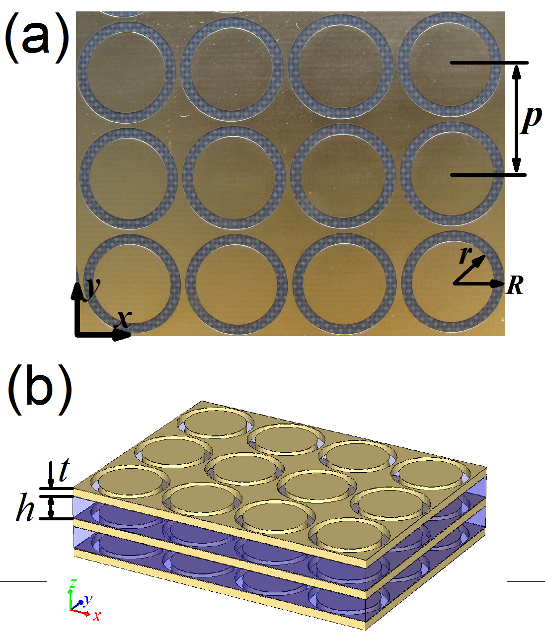
A model system with metallic layers perforated with square arrays of CAAs is of our interest. Figure 1 presents the top-view photo and schematic configuration of a sample with three thin metallic layers( and two sandwiched dielectric space layers. The aperture arrays deposited on different layers are aligned with no displacement in plane. The geometric parameters are the lattice constant of square arrays, the outer radius and inner radius of CAAs, and the thickness of metallic layer respectively. Each dielectric layer has a thickness of and a permittivity of .
Under assumption of perfect electric conductor (PEC) for metals, the electromagnetic wave fields within a metallic layer only exist in apertures. In cylindrical coordinate system, the radial and angular field components and inside an aperture of the metallic layer can be analytically expressed as the superposition of guided resonance modes in the apertures
| (1) |
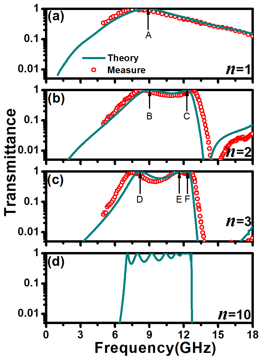
where and are the coefficients of forward and backward guided waves inside the CAAs, and are the order modal functions of radial and angular components in aperture with and being the order Bessel and Neumann functions, refers to the root of the equation . By adopting EQ. (1) as expressions of EM fields in metallic layers and plane-waves as those in dielectric layers, we perform MEM to resolve the electromagnetic problems in the multilayered system. The method is quickly convergent by considering only 2 or 3 lowest guided resonance modes of CAAs. A higher order resonance mode contributes little to the interlayer coupling as its wave vector is a large imaginary number. Three guided modes( in CAAs and orders of plane-wave basis in dielectric layers are adopted in our calculations. The results are very accurate (solid lines in Fig.2) and in good agreement with the measurements (circular dots in Fig.2).
We see from Fig. 2(a) that there exists a transmission peak for the n=1 sample at due to the excitation of guided resonance mode in CAAs. We also see from Figs. 2(b) and 2(c) that there are two transmission peaks at , and for the sample, three peaks at , and for the sample. Figure 2(d) presents the calculated transmission spectra of an n=10 model system. It means that, with the increase of metallic layers, more transmission peaks emerge, giving rise to a broad transparent band.
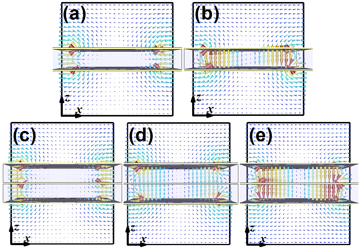
More calculations show that, for the sample, at an on-resonance frequency or where transmissivity is nearly unity, the spatial distribution of electric fields [see Figs. 3(a) and 3(b)] are symmetric or anti-symmetric about the plane. And the transmitted waves possess a phase difference of (in phase) or (out phase) with respect to the incident waves. Therefore the peaks at and , derived from the peak at of the model, come from the excitation and hybridization of the guided resonance mode in apertures at different metallic layers as a results of mode splitting of coupled apertures (or meta-atoms). Further more, the anti-symmetric mode at of the model splits into two modes of the model: spatial field distribution of the one at reveals that the incident and outgoing waves are out phase to each other [Fig. 3(d)] and it is on the opposite for the other at [Fig. 3(e)], while the resonant mode at the lowest frequency retains a symmetric feature in field distribution [Fig. 3(c)] and inherits the in-phase signature from the symmetric mode at of the model.
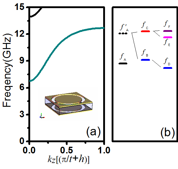
Figure 4(a) presents the dispersion relation of bulk material periodically constructed with layered CAAs. The band structure is calculated with MEM algorithm by assuming periodic boundary conditions along the axis. The process of mode splitting from to , as shown in Fig. 4(b), depicts the evolution of the enhanced transmission feature from a single transmission peak to a broad passband. It is interesting that the passband between and shown in Fig. 4(a), predicting the passband of the model quite well, is also a good measure of the bandwidth of the n=3 sample. The total bandwidth is about 60% of the central frequency. In contrast, the EOT observed in multilayered systems of previous studies demonstrates a peak lineshape in spectra as it arises from the resonant tunneling of SPP modes among metallic films instead of guided resonance modes. And the broad passband we observed is not sensitive to the incident angle (not shown), while it is on the contrary when the SPP modes dominate.
In summary, we present a first report on broadband enhanced transmission through stacked metallic multi-layers perforated with CAAs. Taking advantage of the excitation and interlayer coupling of guided resonance modes of CAAs, the enhanced transmission of such a system with only three metallic layers can span a wide frequency range covering about 60% of the central frequency. The broadband utility shall have enormous potential applications in optoelectronics, telecommunication and image processing.
This work was supported by NSFC (No. 10974144, 60674778), CNKBRSF (Grant No. 2011CB922001), the National 863 Program of China (No.2006AA03Z407), NCET (07-0621), STCSM and SHEDF (No. 06SG24).
References
- (1) T. W. Ebbesen, H. J. Lezec, H. F. Ghaemi, T. Thio, and P. A. Wolff, Nature 391, 667 (1998).
- (2) L. Martin-Moreno, F. J. Garcia-Vidal, H. J. Lezec, K. M. Pellerin, T. Thio, J. B. Pendry, and T. W. Ebbesen, Phys. Rev. Lett. 86, 1114 (2001).
- (3) F. J. G. de Abajo and J. J. Saenz, Phys. Rev. Lett. 95, 233901 (2005).
- (4) G. Gay, O. Alloschery, B. V. de Lesegno, J. Weiner, and H. J. Lezec, Phys. Rev. Lett. 96, 213901 (2006).
- (5) H. T. Liu and P. Lalanne, Nature 452, 728 (2008).
- (6) X. A. Xiao, W. Jinbo, Y. Sasagawa, F. Miyamaru, M. Y. Zhang, M. W. Takeda, C. Y. Qiu, W. J. Wen, and P. Sheng, Opt. Express 18, 18558 (2010).
- (7) Y. M. Bahk, H. R. Park, K. J. Ahn, H. S. Kim, Y. H. Ahn, D. S. Kim, J. Bravo-Abad, L. Martin-Moreno, and F. J. Garcia-Vidal, Phys. Rev. Lett. 106, 013902 (2011).
- (8) H. Raether, Surface Plasmons on Smooth and Rough Surfaces and on Gratings (Springer-Verlag, Berlin, 1988).
- (9) W. L. Barnes, A. Dereux, and T. W. Ebbesen, Nature 424, 824 (2003).
- (10) F. Miyamaru and M. Hangyo, Phy. Rev. B 71, 165408 (2005).
- (11) Y. H. Ye and J. Y. Zhang, Opt. Lett. 30, 1521 (2005).
- (12) H. B. Chan, Z. Marcet, K. Woo, D. B. Tanner, D. W. Carr, J. E. Bower, R. A. Cirelli, E. Ferry, F. Klemens, J. Miner, C. S. Pai, and J. A. Taylor, Opt. Lett. 31, 516 (2006).
- (13) Z. H. Tang, R. W. Peng, Z. Wang, X. Wu, Y. J. Bao, Q. J. Wang, Z. J. Zhang, W. H. Sun, and M. Wang, Phy. Rev. B 76, 195405 (2007).
- (14) R. Ortuno, C. Garcia-Meca, F. J. Rodriguez-Fortuno, J. Marti, and A. Martinez, Phy. Rev. B 79, 075425 (2009).
- (15) Z. Marcet, Z. H. Hang, C. T. Chan, I. Kravchenko, J. E. Bower, R. A. Cirelli, F. Klemens, W. M. Mansfield, J. F. Miner, C. S. Pai, and H. B. Chan, Opt. Lett. 35, 2124 (2010).
- (16) L. Zhou, C. P. Huang, S. Wu, X. G. Yin, Y. M. Wang, Q. J. Wang, and Y. Y. Zhu, Appl. Phys. Lett. 97, 011905 (2010).
- (17) H. M. Su, Z. H. Hang, Z. Marcet, H. B. Chan, C. T. Chan, and K. S. Wong, Phy. Rev. B 83, 245449 (2011).
- (18) F. I. Baida, D. Van Labeke, G. Granet, A. Moreau, and A. Belkhir, Appl. Phys. B: Lasers Opt. 79, 1 (2004).
- (19) W. J. Fan, S. Zhang, K. J. Malloy, and S. R. J. Brueck, Opt. Express 13, 4406 (2005).
- (20) W. J. Fan, S. Zhang, B. Minhas, K. J. Malloy, and S. R. J. Brueck, Phys. Rev. Lett. 94, 033902 (2005).
- (21) K. L. van der Molen, K. J. Klein Koerkamp, S. Enoch, F. B. Segerink, N. F. van Hulst, and L. Kuipers, Phy. Rev. B 72, 045421 (2005).
- (22) W. J. Wen, L. Zhou, B. Hou, C. T. Chan, and P. Sheng, Phy. Rev. B 72, 153406 (2005).
- (23) Z. Y. Wei, J. X. Fu, Y. Cao, C. Wu, and H. Q. Li, Photonics Nanostruct. 8, 94 (2010).
- (24) Z. C. Ruan and M. Qiu, Phys. Rev. Lett. 96, 233901 (2006).
- (25) P. Sheng, R. S. Stepleman, and P. N. Sanda, Phy. Rev. B 26, 2907 (1982).
- (26) P. Lalanne, J. P. Hugonin, S. Astilean, M. Palamaru, and K. D. Moller, J. Opt. a-Pure Appl. Op. 2, 48 (2000).
- (27) Z. Y. Wei, Y. Cao, J. Han, C. Wu, Y. C. Fan, and H. Q. Li, Appl. Phys. Lett. 97, 141901 (2010). Z. Y. Wei, H. Q. Li, Y. Cao, C. Wu, J. Z. Ren, Z. H. Hang, H. Chen, D. Z. Zhang, and C. T. Chan, New J. Phys. (2010).Z. Y. Wei, H. Q. Li, C. Wu, Y. Cao, J. Z. Ren, Z. H. Hang, H. Chen, D. Z. Zhang, and C. T. Chan, Opt. Express 18, 12119 (2010).