Observations of two-dimensional quantum oscillations and ambipolar transport in the topological insulator Bi2Se3 achieved by Cd doping
Abstract
We present a defect-engineering strategy to optimize the transport properties of the topological insulator Bi2Se3 to show a high bulk resistivity and clear quantum oscillations. Starting with a -type Bi2Se3 obtained by combining Cd doping and a Se-rich crystal-growth condition, we were able to observe a -to--type conversion upon gradually increasing the Se vacancies by post annealing. With the optimal annealing condition where a high level of compensation is achieved, the resistivity exceeds 0.5 cm at 1.8 K and we observed two-dimensional Shubnikov-de Haas oscillations composed of multiple frequencies in magnetic fields below 14 T.
pacs:
73.25.+i, 74.62.Dh, 72.20.My, 73.20.AtI Introduction
The three-dimensional (3D) topological insulator (TI) realizes a novel quantum state of matter where a nontrivial topology of the wavefunction of the bulk valence band leads to the emergence of a “topological” surface state consisting of helically spin-polarized Dirac fermions.K2 ; MB ; Roy The peculiar spin texture of the surface state holds promise for novel spintronics and fault-tolerant topological quantum computing, so there is a rush of research to address this surface state.Kane ; ZhangSC However, most of the known TI materials are poorly insulating in the bulk, making it difficult to probe the surface state by transport experiments. For example, Bi2Se3 is considered to be a promising TI material because it has a relatively large (0.3 eV) bulk band gap and a nearly perfect Dirac cone as its topological surface state;ZhangH ; Xia however, no matter whether it is in the form of bulk crystal,Xia ; Eto nanoribbon,Peng or epitaxial thin film,Xue Bi2Se3 always accompanies a lot of Se vacancies (usually 1019 cm-3) that act as electron donors, and as a result, the residual bulk carriers hinder the transport studies of the surface state of this material.
To achieve a bulk-insulating state in Bi2Se3, doping holes to compensate for the residual electrons is a viable strategy. While this was done through low-level substitution of Ca2+ for Bi3+,Hor the resulting disorder was so strong that no Shubnikov-de Haas (SdH) oscillation from the surface state was observedCheckelsky in Bi2-xCaxSe3. A different strategy was to partially substitute Sb for Bi, which apparently reduces the Se vacancies; indeed, with a relatively large (12%) Sb substitution, surface SdH oscillations were successfully observed in -type Bi2-xSbxSe3, but a very high magnetic field (60 T) was required for the observation.Analytis1 It is to be noted that with the Sb doping one can never cross the band gap to reach the -type regime, and hence the tuning of the chemical potential to the Dirac point is impossible. This is a pity, because Bi2Se3 is attractive for its isolation of the Dirac point from the bulk bands. Therefore, it is desirable to find a suitable -type dopant to access the Dirac point while keeping the mobility to be sufficiently high for the surface state to be studied by the SdH oscillations.
In this paper, we show that tactful defect engineering in Bi2Se3 employing Cd doping in combination with Se-vacancy tuning provides a useful means to control the chemical potential across the band gap. In the literature,Horak whereas Cd in Bi2Se3 was shown to behave as an acceptor, Cd-doped Bi2Se3 crystals always remained -type due to the low solubility of Cd atoms in Bi2Se3; however, it has been elucidatedkohler ; Analytis2 ; Butch that increasing the Se content in the Bi-Se melt for the crystal growth can suppress the formation of Se vacancies and greatly reduce the residual bulk carrier density to the level of 1017 cm-3. Therefore, even though the solubility of Cd is low, one could achieve a -type behavior by combining Cd doping and a Se-rich growth condition. Actually, we obtained a -type sample with this strategy and, furthermore, starting from the -type sample, we could gradually increase the Se vacancies by careful post-annealing and achieve a high level of compensation, at which the sample becomes optimally bulk-insulating and presents two-dimensional (2D) SdH oscillations below 14 T.
II Experimental Details
The single crystals of Cd-doped Bi2Se3 were grown by using elemental shots of Bi (99.9999%), Cd (99.99%) and Se (99.999%) as starting materials. To maximize the Cd content in the crystal, excess Cd and a mixture of Bi and Se with a ratio of Bi:Se = 32:68 were melted in a sealed evacuated quartz tube at 750 ∘C for 48 h with intermittent shaking to ensure a homogeneity, followed by cooling slowly to 550 ∘C and then annealing at the same temperature for one week. The resulting crystals are easily cleaved along the basal plane, revealing a silvery mirror-like surface. The X-ray diffraction measurements confirmed the crystal to be single phase with the proper Bi2Se3 structure. The actual Cd content was determined by the inductively-coupled plasma atomic-emission spectroscopy (ICP-AES) to be 0.0020(2). The as-grown crystals were examined by X-ray Laue analysis and cut into single-domain, thin bar-shaped samples with typical dimensions of 310.2 mm3.
For each annealing experiment, samples weighing about 4.2 mg were sealed in evacuated quartz tubes and annealed at a given temperature for one week, followed by quenching into cold water. All the samples used in this work were taken from the same part of the same batch, and the variation of the Cd content was confirmed to be negligible by the ICP-AES analysis. To avoid possible surface contamination, the surface layer of the annealed crystals were removed using adhesive tapes before transport measurements.
It worth mentioning that in our annealing experiments, we took precautions to minimize the uncertainty in the annealing temperature. For each annealing run, we placed the quartz tube at the same position of the same furnace so that the temperature gradients in the furnace as well as the thermocouple calibration errors do not affect the annealing result. Also, the environment temperature was kept constant during this experiment to minimize the temperature fluctuations between different annealing runs. As a result, the annealing temperature was very reproducible and its variation between different runs with nominally the same was within 1 ∘C.
The in-plane resistivity and the Hall coefficient were measured in a Quantum Design Physical Properties Measurement System (PPMS-9) down to 1.8 K, for which the electrical contacts were prepared by using room-temperature-cured silver paste. In addition, one of the high-resistivity samples was brought to a 14-T magnet for detailed SdH-oscillation measurements using an ac six-probe method, in which four lock-in amplifiers were employed to measure both the primary and the second-harmonic signals in the longitudinal and transverse channels at a frequency of 19 Hz. The SdH-oscillation data were taken by sweeping the magnetic fields between 14 T with the rate of 0.3 T/min, during which the temperature was stabilized to within 5 mK.
III Results and Discussions
III.1 -type Bi2-xCdxSe3
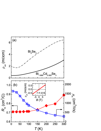
The temperature dependence of the in-plane resistivity of a Bi1.998Cd0.002Se3 crystal grown in the Se-rich condition is shown in Fig. 1(a), together with the data for a pristine Bi2Se3 sample grown with the same Bi/Se ratio. The pristine Bi2Se3 crystal shows an essentially metallic behavior with a weak resistivity upturn below 30 K, which is typical for low-carrier-density Bi2Se3; kohler ; Analytis2 ; Butch indeed, the Hall coefficient in this sample at 1.8 K corresponds to the bulk electron density 71017 cm-3, which is very small for Bi2Se3. On the other hand, in Bi1.998Cd0.002Se3 the resistivity upturn is absent and the value is lower, suggesting a higher carrier density. In fact, as shown in Fig. 1(b), in the Bi1.998Cd0.002Se3 crystal is positive and its value at 1.8 K corresponds to the hole density 91018 cm-3, implying that the Cd doping has created 9.71018 cm-3 of holes (0.8 hole per Cd atom) that outnumbers the electrons coming from Se vacancies.Horak The reason for the smaller number of doped holes compared to the Cd concentration is most likely that a small portion of Cd atoms occupy the interstitial site and act as donors. In Fig. 1(b), is only weakly dependent on temperature and the Hall resistivity is perfectly linear in (as shown in the inset), reflecting the metallic nature of the as-grown Bi1.998Cd0.002Se3 sample which is due to a single type of carriers (i.e., the bulk holes). The Hall mobility (= /), also shown in Fig. 1(b), increases with decreasing temperature, reaching 1600 cm2/Vs at 1.8 K.
III.2 -to--type conversion by post annealing
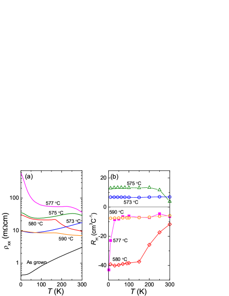
Annealing the as-grown Bi1.998Cd0.002Se3 crystals in evacuated quartz tubes has a drastic effect on its transport properties. Figure 2(a) shows how the temperature dependence of changes upon annealing in a narrow temperature window between 573 and 590 ∘C. One can see that () evolves nonmonotonically with the annealing temperature, ; namely, initially increases with until exceeds 577 ∘C, after which decreases as is further increased. Notably, of the sample annealed at 577 ∘C show a high value of 0.5 cm at 1.8 K, which is three orders of magnitude larger than that of the as-grown sample. Figure 2(b) shows the typical temperature dependences of low-field data (defined as = / for 0) for different , which indicates that more and more electron carriers are introduced as is increased, and the sign change from -type to -type occurs around = 577 ∘C.
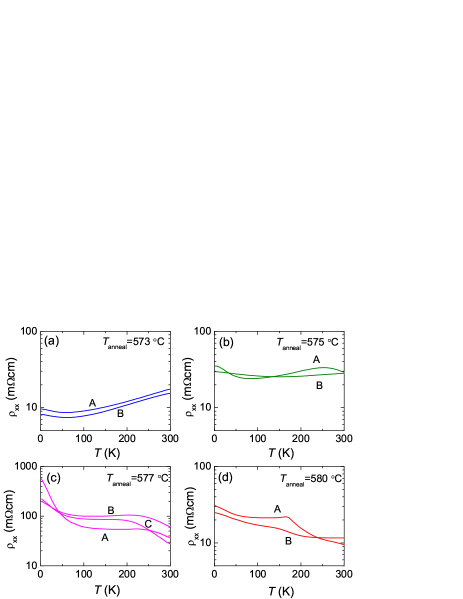
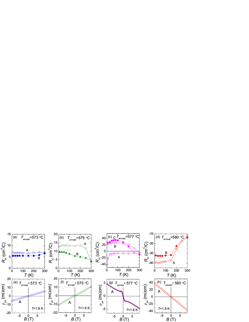
Since the drastic change in the transport properties occurs in a very narrow temperature window (573 – 580 ∘C), one may wonder about the reproducibility of the result. As a matter of fact, the observed change was quite reproducible, as demonstrated in Figs. 3 and 4. Figures 3(a)-3(d) show the data for at least two samples annealed at the same temperature, where one can see that the behavior for each is essentially reproducible. Figures 4(a)-4(d) show the corresponding data for the same sets of samples; here, except for the case of = 577 ∘C [Fig. 4(c)], we observed reasonable reproducibility [Figs. 4(a), 4(b), and 4(d)]. For = 577 ∘C, two of the three samples (A and B) showed a sign change in from negative to positive upon lowering temperature from 300 K, whereas the of sample C remained negative in the whole temperature range. Actually, this variation in the behavior of indicates that the = 577 ∘C samples are at the verge of the -to--type conversion.
Figures 4(e)-4(h) show the curves measured in sample “A” of each . One can clearly see that the curve in Fig. 4(g) for = 577 ∘C is nonlinear, indicating that there are at least two bands contributing to the transport. In topological-insulator samples with a large bulk resistivity, this kind of nonlinear curves are indications of the surface channels making noticeable contributions.BTS_Rapid ; Steinberg ; Qu ; Oh ; BSTS_PRL Therefore, the consistently high resistivity [Fig. 3(c)] together with the complex behaviors of the Hall signal are likely to be a signature of a high level of compensation achieved in the samples annealed at 577 ∘C; in other words, in those samples the acceptors and donors are nearly equal in number and their delicate balance can easily change the sign of . It is to be emphasized that our data demonstrate that this high level of compensation is reproducibly achieved with = 577 ∘C. In samples annealed at other temperatures, the behavior is almost linear [Figs. 4(e), 4(f), and 4(h)], suggesting that the contribution of the surface to the transport properties is minor. In passing, the collection of and data shown in Fig. 2 for varying are for sample “A” of each shown in Figs. 3 and 4.
III.3 Defect chemistry
The above observation that a drastic change in the transport properties of Bi1.998Cd0.002Se3 occurs in a very narrow temperature window might seem surprising. However, this behavior can be readily understood by examining the defect chemistry associated with the annealing. In the present system, there are mainly two different types of charged defects, the aliovalent substitutional defect Cd and the vacancy defect ,Hor ; Horak the former acts as an acceptor and the latter as a donor. Therefore, the effective charge-carrier density is determined by their competition and can be expressed as = , where positive (negative) denotes the hole (electron) density. In an as-grown sample, the Cd defects are dominant and is positive; accordingly, the chemical potential lies in the valence band. When annealed in evacuated quartz tubes, a portion of selenium goes into the gas phase Se2 in equilibrium with the solid phase,cafaro resulting in the formation of more defects while leaving Cd unaffected (because the employed in the present study is much lower than the melting temperature of 710 ∘C). The equilibrated vapor pressure of Se2 increases with increasing , cafaro creating more and eventually changing from positive to negative.
To be more quantitative, one may assume that the increase in the Se-vacancy concentration upon annealing, , is directly reflected in the increase in the number of Se2 molecules in the quartz tube, which determines the Se2 vapor pressure ; in constant volume, one expects a linear relation between and if the Se2 vapor behaves as an ideal gas. According to Ref. cafaro, , the equilibrated Se2 vapor pressure of Bi2Se3 is related to the absolute temperature via
| (1) |
where = 7.810.50 and = 10870640 for the temperature range of 527 to 627 ∘C. From this dependence of , one can infer that is very sensitive to the change in : For example, changing by just 1 ∘C near 577 ∘C results in a variation of 3.5% in ; therefore, the expected change in upon changing from 575 to 580 ∘C is as much as 18%. It is thus expected that a sign change in occurs abruptly in the vicinity of = 577 ∘C where 0 (namely, [] []), and results in a drastic change in the transport properties as we observed.
III.4 Surface quantum oscillations
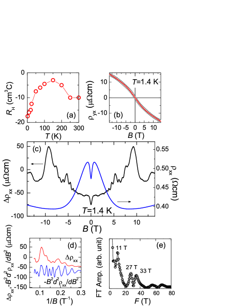
From the above results, it is clear that the highest level of compensation is achieved in samples annealed at 577 ∘C. We therefore measured the sample C of = 577 ∘C in a 14-T magnet using a rotation sample holder to investigate its SdH oscillations in detail. Before the high-field measurements, to protect the surface state from aging, the top surface of the sample was covered with Al2O3 in the following way: first, the crystal was cleaved on both surfaces with adhesive tapes to reveal fresh surfaces, mounted on a sample holder with GE varnish, and transferred into the sputtering chamber; second, the top surface was cleaned by bias-sputtering with Ar ions for 13 minutes and then, without breaking the vacuum, a 540-nm-thick Al2O3 film was deposited by the rf magnetron sputtering. After this process, gold wires were bounded to the side faces by spot welding. Probably because of the sample heating during the spot welding, the value of this sample became even larger than that shown in Fig. 3(c). Also, the sign of at low temperature changed to negative after the process, showing the Hall response similar to that of the sample A. The behavior of this sample C after the Al2O3-coverage process is shown in Fig. 5(a), and its curve at 1.4 K is shown in Fig. 5(b).
In our measurements using an ac lock-in technique, we simultaneously recorded the primary and the second-harmonic signals during the magnetic-field sweeps. Figure 5(c) shows the magnetic-field () dependences of the primary signal () and the second-harmonic signal (denoted ) measured at 1.4 K in magnetic fields along the axis. One can see that the second-harmonic signal () shows pronounced oscillations, while in the primary signal () the oscillations are hardly visible. To understand the nature of the oscillations, we show in Fig. 5(d) the plots of and (second derivative of the primary signal) vs the inverse magnetic field ; a comparison between the two curves indicates that they present essentially the same peak/dip positions. While the waveforms are quite complicated, the Fourier transform (FT) spectrum of shown in Fig. 5(e) presents three well-defined peaks at = 11 T, = 27 T, and = 33 T, indicating that the observed oscillations are SdH oscillations with multiple frequencies.
Note that the second-harmonic in ac measurements is a distortion of the input sine wave, and its occurrence is an indication of a nonlinear response. In the present case, the SdH oscillations are apparently giving rise to a peculiar non-ohmicity. This makes the second-harmonic signal to be useful for observing the SdH oscillations with a high sensitivity, although the detailed mechanism is not clear at the moment.
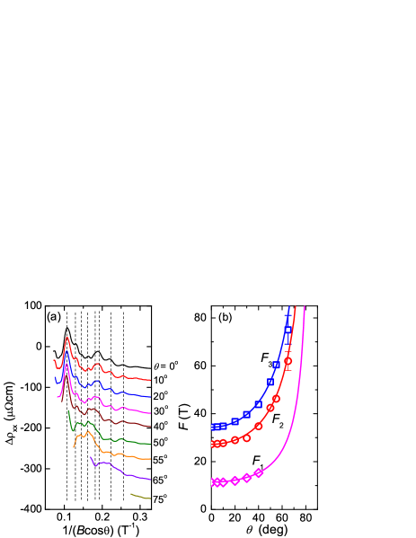
Figure 6(a) shows how the SdH oscillations observed in change when the magnetic field is rotated, by plotting versus where is the angle between and the axis. One can see that the oscillatory features are essentially dependent on the perpendicular component of the magnetic field. Also, as shown in Fig. 6(b), the angular dependences of all three frequencies in the FT spectra are consistent with . These results strongly suggest that the present SdH oscillations signify 2D Fermi surface(s). We note that the SdH oscillations in this sample disappeared after keeping the sample in ambient atmosphere for a week, which suggests that the SdH oscillations were coming from the surface. (This observation also suggests that the Al2O3 coverage, while useful for slowing the aging of the surface of Bi2Se3, does not provide a perfect protection). Furthermore, one can estimate the bulk mobility of this sample to be 40 cm2/Vs from the values of and , and such a mobility is too low to give rise to SdH oscillations of the bulk carriers below 14 T. All told, one can reasonably conclude that the observed SdH oscillations are of the surface origin.
From the SdH-oscillation data, the Fermi wave vector can be calculated via the Onsager relation = , yielding = 0.018, 0.029, and 0.032 Å-1 for , , and , respectively. These are of the same order as the value = 0.031 Å-1 reported for the topological surface state in -type Bi2-xSbxSe3.Analytis1 However, because of the multi-component nature of the oscillations that leads to complicated waveforms, it is difficult to reliably extract the cyclotron mass nor the Dingle temperature for each component using the Lifshitz-Kosevich theory.Shoenberg1984 This makes it impossible to identify the origins of the three oscillation frequencies, but possible reasons for the multiple components in the present case include: (i) harmonics of a fundamental frequency are observed, (ii) chemical potentials of the top and bottom surfaces are not identical and give two frequencies associated with the topological surface states, (iii) a trivial 2D electron gas Bianchi created by the band bending at the surface presents additional SdH oscillations. Note that, in the case of the present sample used for the detailed SdH measurements, the top surface was covered by Al2O3 and the bottom surface was covered by the GE varnish, so the conditions of the two surfaces were very different. To resolve the origins of those multiple frequencies, an experiment involving the gate control of the surface chemical potential to trace the energy dispersion of each branch (as was done Sacepe for exfoliated Bi2Se3) would be desirable.
III.5 Nonlinear behavior
Although we could not extract the surface mobility from the SdH oscillations in the present case, we can still estimate the relevant parameters of the surface and the bulk transport channels by analyzing the nonlinear behavior [Fig. 5(b)] with the simple two-band model described in Ref. BTS_Rapid, . The solid line in Fig. 5(b) is the result of the two-band-model fitting, from which we obtained the bulk electron density = 71017 cm-3, the bulk mobility = 17 cm2/Vs, the surface electron density = 1.81012 cm-2, and the surface mobility = 1.2103 cm2/Vs. The observed frequencies of the SdH oscillations, 11, 27, and 33 T correspond to the surface carrier densities of 2.51011, 6.71011, and 8.11011 cm-2 in spin-filtered surface states, respectively, and it is interesting that the sum of these numbers, 1.71012 cm-2, appears to be consistent with the value obtained from the two-band analysis. Also, it is assuring that the surface mobility obtained from the two-band analysis, 1200 cm2/Vs, is reasonably large and is consistent with our observation of the SdH oscillations in moderate magnetic fields.
In passing, the data of the sample A shown in Fig. 4(g) can also be fitted with the two-band model. The result of the fitting, shown by the solid line in Fig. 4(g), yields the bulk electron density = 1.31018 cm-3, the bulk mobility = 15 cm2/Vs, the surface electron density = 2.01011 cm-2, and the surface mobility = 1.0104 cm2/Vs for this sample.
IV Conclusion
In conclusion, we demonstrate that with tactful defect engineering one can optimize the transport properties of the topological insulator Bi2Se3 to show a high bulk resistivity and clear quantum oscillations. Specifically, by employing a Se-rich crystal-growth condition we achieved the -type state in Bi2Se3 by Cd-doping for the first time; we then employed careful post annealing to tune the Se vacancies and achieved a high level of compensation, where the acceptors and donors nearly cancel each other and the sample presents a high value exceeding 0.5 cm at 1.8 K and shows 2D SdH oscillations consisting of multiple components below 14 T.
Acknowledgements.
We thank T. Minami for technical assistance. This work was supported by JSPS (NEXT Program and KAKENHI 19674002), MEXT (Innovative Area “Topological Quantum Phenomena” KAKENHI 22103004), and AFOSR (AOARD 10-4103).References
- (1) L. Fu and C.L. Kane, Phys. Rev. B 76, 045302 (2007).
- (2) J.E. Moore and L. Balents, Phys. Rev. B 75, 121306(R) (2007).
- (3) R. Roy, Phys. Rev. B 79, 195322 (2009).
- (4) M.Z. Hasan and C.L. Kane, Rev. Mod. Phys. 82, 3045 (2010).
- (5) X.L. Qi and S.C. Zhang, arXiv:1008.2026.
- (6) H.J. Zhang, C.X. Liu, X.L. Qi, X. Dai, Z. Fang, and S.C. Zhang, Nat. Phys. 5, 348 (2009).
- (7) Y. Xia, D. Qian, D. Hsieh, L. Wray, A. Pal. H. Lin, A. Bansil, D. Grauer, Y.S. Hor, R.J. Cava, and M.Z. Hasan, Nat. Phys. 5, 398 (2009).
- (8) K. Eto, Z. Ren, A.A. Taskin, K. Segawa, and Y. Ando, Phys. Rev. B 81, 195309 (2010).
- (9) H. Peng, K. Lai, D. Kong, S. Meister, Y. Chen, X.L. Qi, S.C. Zhang, Z.X. Shen, and Y. Cui, Nat. Mater. 9, 225 (2010).
- (10) X. Chen, X.C. Ma, K. He, J.F. Jia, and Q.K. Xue, Adv. Mat. 23, 1162 (2011).
- (11) Y.S. Hor, A. Richardella, P. Roushan, Y. Xia, J.G. Checkelsky, A. Yazdani, M.Z. Hasan, N.P. Ong, and R.J. Cava, Phys. Rev. B 79, 195208 (2009).
- (12) J.G. Checkelsky, Y.S. Hor, M.H. Liu, D.X. Qu, R.J. Cava, and N.P. Ong, Phys. Rev. Lett. 103, 246601 (2009).
- (13) J.G. Analytis, R.D. McDonald, S.C. Riggs, J.H. Chu, G.S. Boebinger, and I.R. Fisher, Nat. Phys. 6, 960 (2010).
- (14) J. Horák, L. Koudelka, J. Kilkorka, and L. Šiška, Phys. Status Solidi 111, 575 (1982).
- (15) H. Köhler and A. Fabricius, Phys. Status Solidi B 71, 487 (1975).
- (16) J.G. Analytis, J.H. Chu, Y. Chen, F. Corredor, R.D. McDonald, Z.X. Shen, and I.R. Fisher, Phys. Rev. B 81, 205407 (2010).
- (17) N.P. Butch, K. Kirshenbaum, P. Syers, A.B. Sushkov, G.S. Jenkins, H.D. Drew, and J. Paglione, Phys. Rev. B 81, 241301(R) (2010).
- (18) Z. Ren, A.A. Taskin, S. Sasaki, K. Segawa, and Y. Ando, Phys. Rev. B 82, 241306(R) (2010).
- (19) H. Steinberg, D.R. Gardner, Y.S. Lee, P. Jarillo-Herrero, Nano Lett. 10, 5032 (2010).
- (20) D.-X. Qu, Y.S. Hor, J. Xiong, R.J. Cava and N.P. Ong, Science 329, 821 (2010).
- (21) N. Bansal, Y.S. Kim, M. Brahlek, E. Edrey, S. Oh, arXiv:1104.5709.
- (22) A.A. Taskin, Z. Ren, S. Sasaki, K. Segawa, and Y. Ando, Phys. Rev. Lett. (to be published), arXiv:1105.5483.
- (23) M. L. Cafaro, G. Bardi, and V. Oiancente, J. Chem. Eng. Data 29, 78 (1984).
- (24) D. Shoenberg, Magnetic Oscillations in Metals (Cambridge University Press, Cambridge, 1984).
- (25) M. Bianchi, D.D. Guan, S.N. Bao, J.L. Mi, B.B. Iversen, P.D.C. King, and P. Hofmann, Nat. Commun. 1, 128 (2010).
- (26) B. Sacépé, J.B. Oostinga, J. Li, A. Ubaldini, N.J.G. Couto, E. Giannini, and A.F. Morpurgo, arXiv:1101.2352.