Coexistence of electron and hole transport in graphene
Abstract
When sweeping the carrier concentration in monolayer graphene through the charge neutrality point, the experimentally measured Hall resistivity shows a smooth zero crossing. Using a two-component model of coexisting electrons and holes around the charge neutrality point, we unambiguously show that both types of carriers are simultaneously present. For high magnetic fields up to 30 T the electron and hole concentrations at the charge neutrality point increase with the degeneracy of the zero-energy Landau level, which implies a quantum Hall metal state at =0 made up by both electrons and holes.
pacs:
73.43.-f, 73.63.-b, 71.70.DiI Introduction
The carrier concentration in semiconductors is commonly measured using the Hall effect based on the Lorentz force exerted on moving charged particles in a perpendicular magnetic field Hall . In conventional finite-gap semiconductors, the low-temperature Hall resistivity directly measures either the electron or the hole density. However, in compensated semiconductors, where electrons and holes coexist, the Hall resistivity is determined by both types of carriers and, in particular, becomes zero in a fully compensated material.
Graphene is an ideal two-dimensional zero-gap semiconductor with a linear dispersion Rise of graphene where the electron and hole concentration at =0 go to zero when sweeping the carrier density through the charge neutrality point (CNP). However, non-perfect samples with random potential fluctuations will break up into spatially inhomogeneous conducting electron-hole puddles Yacobi-puddles leaving a finite number of electrons and holes directly at the CNP.
In this article, we present experimental results on the Hall resistivity in graphene around the CNP in magnetic fields up to 30 T and for temperatures down to 0.5 K. We demonstrate that the smooth zero-crossing of at the CNP for all magnetic fields is caused by a finite concentration of both electrons and holes below and above the CNP with an equal number of electron and hole states occupied at the CNP. We show that the measured carrier concentration increases linearly with the magnetic field which is related to the degeneracy of the zero-energy LL shared equally between electrons and holes.
We have investigated three different graphene devices made from Kish graphite (sample A) and natural graphite (samples B and C) with mobilities between m2V-1s-1 for sample A and m2V-1s-1 for samples B and C. Single-layer graphene flakes were deposited on a Si/SiO2 substrate, identified optically Blake and patterned using standard techniques ScienceKostya-Device ; Rise of graphene . The total charge-carrier concentration in the graphene films, defined as , can be adjusted from hole-doped () to electron doped () by means of a back-gate voltage . Here and are the carrier concentrations for electrons and holes, respectively, and mV-1 for a 300-nm thick SiO2 gate insulator. In order to remove surface impurities, all devices were annealed at 440 K prior to the low-temperature measurements. Admixtures of to due to contact misalignment and inhomogeneities we removed by symmetrization of all traces measured in positive and negative magnetic fields.
The paper is organized as follows: Section II presents our experimental results. The first part of Section II shows transport measurements at low magnetic fields where the Hall resistance is not yet quantized and charge carriers can be considered as “free” (mobile). The second part presents data up to 30 T in the quantum Hall (QH) regime. Section III develops a model for the density of states in graphene, first applied to our samples and then we discuss different splitting scenarios of the lowest Landau level. Concluding remarks are given in the last section.
II Experimental results
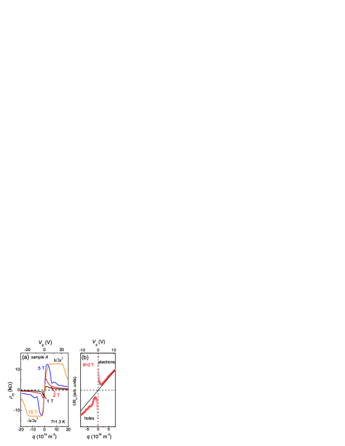
We first present measurements of Hall resistivity with increasing magnetic field in Fig. 1(a) for sample A as a function of total carrier concentration for several magnetic fields at =1.3 K. The corresponding back-gate voltage is displayed on the top-axis. For =15 T, exhibits Hall plateaus quantized to at filling factors . For all magnetic fields, the Hall resistance is not diverging at the CNP when either electron or hole states are depleted. rather moves smoothly through zero from the plateau to the =+2 plateau.
In order to accommodate for this simple experimental observation, we describe the inverse Hall coefficient with a two-carrier model for electrons and holes as known for compensated semiconductors two-carrier
| (1) |
and are the electron and hole concentrations and and are the electron and hole mobilities, respectively. In our graphene samples the measured conductivity as a function of carrier concentration is symmetric around the CNP and we can therefore assume the same mobility for both electrons and holes, , and Eq. (1) simplifies to
| (2) |
It is worth emphasizing that we can apply the two-carrier model despite the presence of electron-hole puddles, which would result, for conventional nonrelativistic charge carriers, in spatial separation and related percolation phenomena in electron and hole regions. In the two-dimensional case, the percolation over electron puddles blocks unavoidably the transport for holes, and vice versa. The case of graphene is dramatically different. The crucial point is that for graphene the borders between and regions are actually transparent, and electrons and holes transfer smoothly into each other, which is referred to as Klein tunneling Katsnelson-Klein . At specific magic angles of incidence (including normal incidence) the transmission probability is 100% . The presence of a magnetic field does not destroy the Klein tunneling but just shifts the magic angles Young-Klein . It can be assumed that tunneling from one electron puddle to the other electron puddle always remains possible even for carriers incident to an oblique angle (the same holds for hole transport). Thus, even under a nonuniform distribution of electron-hole puddles, we can apply our two-carrier model to graphene.
Fig. 1(b) shows the inverse Hall coefficient as a function of for =2 T extracted from our measurements. For high , exhibits a linear increase due to the presence of either electrons () or holes (). For , however, the simultaneous presence of two distinct types of charge carriers around the CNP immediately becomes visible as a divergence of around the CNP, which in turn implies that must remain finite.
II.1 Low magnetic fields
We now present low-field data in Fig. 2 for sample B measured at 0.5 K and in magnetic fields where the quantum Hall effect (QHE) is not yet developed. Using Eq. (2) we extract the individual charge-carrier concentrations and as a function of the total charge density [see Fig. 2(b)].
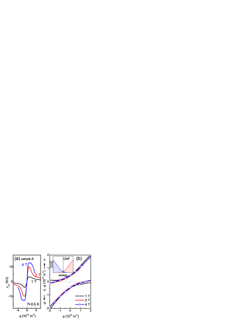
Both charge carriers are present above and below the CNP and the electron (hole) concentration already starts to increase as the hole (electron) concentration is still decreasing. Precisely at the CNP, we extract a charge-carrier concentration m-2 only weakly dependent on for T. Away from the CNP, the system remains two-component and the minority charge carriers only disappear for m-2. The same analysis for the other two samples qualitatively yields similar results with m-2 for sample A and m-2 for sample C. The fact that the sample with the lowest mobility (sample A) reveals the highest qualitatively confirms a scenario of coexisting electron-hole puddles, where lower mobilities are generally associated with larger potential fluctuations.
II.2 Quantum Hall regime
We now turn our attention to measurements in high magnetic fields. We present experimental data from 5 to 25 T both for longitudinal resistivity and Hall resistivity [see Fig. 3(a) and Fig. 3(b)] measured in sample C at =4 K. is measured from =5 T up to 25 T in steps of 5 T. is now quantized at 2 but still shows a smooth zero-crossing from to without any sign of divergence at the CNP. Consequently, we still find a finite charge carrier concentration for electrons and holes around the CNP as depicted in Fig. 3(c). Therefore, we can conclude that electrons still contribute to conduction below =0 and holes do so above =0. It should be noticed that in the range of magnetic fields used for the extraction of the carrier densities, does not affect even if we take into account a small amount of mixing between both signals but becomes relevant if starts diverging at the CNP.
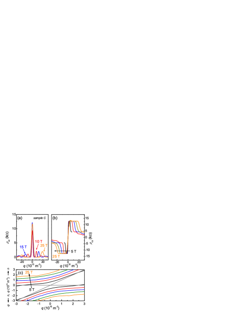
In addition, we now observe an increase of and with increasing magnetic field. This field-dependent carrier concentration around the CNP is elucidated further in Fig. 4 where we plot the electron concentration at the CNP as a function of magnetic field for all investigated samples. For low magnetic fields (5 T), remains constant and can be explained by the presence of electron-hole puddles.
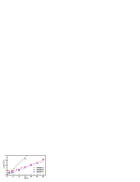
For higher magnetic fields, starts to increase linearly with reflecting the -proportional degeneracy for each of the four sub-levels in the zero-energy Landau level (LL) Kostya-QHE ; Kim-QHE . Since, at the CNP, half of the possible electrons states and half of the hole states are filled, respectively, we expect electron states and hole states occupied per unit area. Therefore, for comparison, we have also plotted in Fig. 4. Interestingly, we only observe about 30 of the expected electron and hole concentration in our data extracted from the Hall experiments.
In contrast to low magnetic fields, where the QHE is not yet developped and all charge carriers can be considered as mobile, we now have to take into account localized charge carriers in the tails of the LLs in the quantized regime. This fact is essentially reflected in Fig. 4, where we extracted the density for electrons and holes using Eq. (2) from the Hall resistivity, which only takes free charge carriers into account. To further support our assumption that about 30 of the charge carriers are indeed free, we take a look at the broadening of LLs and the ratio between extended and localized states depending on the strength of the magnetic field which has been extracted from temperature-dependent measurements Jos-temperature and QH plateaus at high . Indeed, we observe a good agreement with our findings that only 30 of the total carrier concentration is measured as free charge carriers.
III Density of states model
III.1 Investigated samples
The above measurements allow us to sketch the density of states (DOS) for electrons and holes. For =0 (see inset to Fig. 2) the DOS in graphene ( is the Fermi velocity) is smeared out around the CNP due to the presence of electron-hole puddles. Applying a magnetic field leads to a quantization of the DOS, shown in Fig. 5(a). Electrons and holes in the center of the LLs are extended (shaded areas) whereas they are localized in the Landau level tails (filled areas). In that picture the LLs =0 and =1 are well separated, yielding quantized plateaus in at 2 [Fig. 3(a)] when the Fermi energy is situated in the localized tails of the LLs.
Within this DOS model (see also Ref. Jos-gap ) we can now calculate the longitudinal conductivity by means of the Kubo-Greenwood formalism Kubo ; Greenwood and the Hall conductivity summing up all states below the Fermi energy Streda . Including the presence of electrons and holes above and below the CNP indeed yields a smooth zero crossing of as measured in Fig. 3(a) and modeled in Fig. 5(b).

Our experimental observation of coexisting electrons and holes around the CNP also has a direct implication on the nature of the =0 QHE in graphene DasSarma . Neither a gap opening at the CNP Jos-gap , nor a complete lifting of spin and valley degeneracy, if we assume the spin first scenario of the zeroth LL Zhang , fundamentally change the zero-crossing of the Hall resistance. Our experimental results up to a magnetic field of 30 T do not exhibit interaction-driven QHE Nomura due to a larger disorder confirmed by lower mobility in our samples compared to Ref. Zhang . If we calculate and from measured and using standard matrix inversion our samples show the gap opening in at =30 T due to increasing at the CNP. Consequently, a small plateau in at the CNP appears whereas the Hall resistance smoothly crosses through zero Jos-gap .
III.2 Splitting scenarios of the lowest Landau level
In samples with lower disorder, spin and valley degeneracies are lifted. As demonstrated in Ref. Zhang , the Hall resistivity exhibits a smooth zero-crossing (with fluctuations) from the =-1 plateau to the =1 plateau with increasing . We have calculated the DOS assuming that both electrons and holes exist above and below the CNP [Fig. 6(c)] and find the smooth zero-crossing of the Hall resistivity [see Fig. 6(c)].
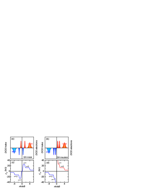
Furthermore, we use our DOS model to directly address the question weather =0 is a QH-metal or a QH-insulator. Measurements of longitudinal resistance have shown either finite , even subjected to high magnetic fields (QH-metal) Kostya-QHE ; Kim-QHE ; Zhang ; Abanin or a steeply increase in , attributed to an insulating ground state Ong . The first observation is generally explained by an insulating bulk and conducting channals at the sample edges Abanin . Both scenarios are directly related to the lifting of degeneracy of the zeroth LL. Whereas in a QH-metal spin splitting is larger than valley splitting, in a QH-insulator the contrary is the case. If spin and valley degeneracy is lifted, a zero-crossing of is observed if we include the presence of electrons and holes above and below the CNP, see Fig. 6(a) and (c). However, if we separate electrons and holes at the CNP, see Fig. 6(b) (valley first scenario), diverges (see Fig. 6(d)). The divergence of in the valley first scenario beyond filling factor =1 when approaching the CNP has indeed been recently found in high mobility graphene devices, fabricated on a single-crystal boron nitride substrate Dean and thus confirm our DOS model. However, beyond fractional filling factor =1/3, starts to decrease strongly and might pass through zero. This behavior would imply positive and negative charged composite fermions around the CNP.
IV Conclusion
In conclusion, we have performed measurements of the Hall resistivity in
graphene in a magnetic field up to 30 T. does not diverge
at the CNP but shows a smooth transition from electrons to holes. Our
analysis based on mixed conduction at the CNP implies that both electrons
and holes exist both below and above the CNP with as many hole states
as electron states occupied at the CNP. Charge-carrier concentration
as a function of magnetic field is explained as a transition from
transport dominated by electron-hole puddles to a quantized DOS
with increasing . Taking into account the presence of both charge
carriers above and below the CNP contributes to a better understanding
of the unique nature of electronic states at the lowest LL in graphene.
Finally, we have to point out that physics around the CNP, such as the
behavior of from hole-dominated to electron-dominated transport
becomes easier to access with high-mobility samples even though diverging
directly affects the extraction of Hall resistivity under realistic
experimental conditions.
Part of this work has been supported by EuroMagNET II under the EU contract number 228043 and by the Stichting Fundamenteel Onderzoek der Materie (FOM) with financial support from the Nederlandse Organisatie voor Wetenschappelijk Onderzoek (NWO).
References
- (1) E. H. Hall, American Journal of Mathematics vol 2, 287 (1879).
- (2) A. K. Geim and K. S. Novoselov, Nat. Mater. 6, 183 (2007).
- (3) J. Martin, N. Akerman, G. Ulbricht, T. Lohmann, J. H. Smet, K. von Klitzing, A. Yacobi, Nat. Phys. 4, 144 (2008).
- (4) P. Blake, E. W. Hill, A. H. Castro Neto, K. S. Novoselov, D. Jiang, R. Yang, T. J. Booth, and A. K. Geim, Appl. Phys. Lett. 91, 063124 (2007).
- (5) K. S. Novoselov, A. K. Geim, S. V. Morozov, D. Jiang, Y. Zhang, S. V. Dubonos, I. V. Grigorieva, and A. A. Firsov, Science 306, 666 (2004).
- (6) see, e.g., K. Seeger, Semiconductor physics, an introduction, 5th ed., p. 61, Springer, Berlin (1997).
- (7) M. I. Katsnelson, K. S. Novoselov, and A. K. Geim, Nature Phys. 2, 620 (2006).
- (8) A. F. Young and P. Kim, Nature Phys. 5, 222 (2009).
- (9) K. S. Novoselov, A. K. Geim, S. V. Morozov, D. Jiang, M. I. Katsnelson, I. V. Grigorieva, S. V. Dubonos, and A. A. Firsov, Nature (London) 438, 197 (2005).
- (10) Y. Zhang, Y. Tan, H. L. Stormer, and P. Kim, Nature (London) 438, 201 (2005).
- (11) A. J. M. Giesbers, U. Zeitler, M. I. Katsnelson, L. A. Ponomarenko, T. M. Mohiuddin, and J. C. Maan, Phys. Rev. Lett. 99, 206803 (2007).
- (12) A. J. M. Giesbers, L. A. Ponomarenko, K. S. Novoselov, A. K. Geim, M. I. Katsnelson, J. C. Maan, and U. Zeitler, Phys. Rev. B 80, 201403(R) (2009).
- (13) R. Kubo, Canad. J. Phys. 34, 1274-1277 (1956).
- (14) D. A. Greenwood, Proc. Phys. Soc. London 71, 585-596 (1958).
- (15) P. Streda, J. Phys. C: Solid. State Phys. 15, 717-721 (1982).
- (16) S. Das Sarma and K. Yang, Solid State Commun. 149, 1502 (2009).
- (17) Y. Zhang, Z. Jiang, J. P. Small, M. S. Purewal, Y. W. Tan, M. Fazlollahi, J. D. Chudow, J. A. Jaszczak, H. L. Stormer, and P. Kim, Phys. Rev. Lett. 96, 136806 (2006).
- (18) K. Nomura and A. H. MacDonald, Phys. Rev. Lett. 96, 256602 (2006).
- (19) D. A. Abanin, K. S. Novoselov, U. Zeitler, P. A. Lee, A. K. Geim, and L. S. Levitov, Phys. Rev. Lett. 98, 196806 (2007).
- (20) J. G. Checkelsky, L. Li, and N. P. Ong, Phys. Rev. Lett. 100, 206801 (2008); Phys. Rev. B 79, 115434 (2009).
- (21) C. R. Dean, A. F. Young, P. Cadden-Zimansky, L. Wang, H. Ren, K. Watanabe, T. Taniguchi, P. Kim, J. Hone, K. L. Shepard, Nature Phys., 5, 693 (2011).