Chiral charge order in the superconductor 2H-TaS2
Abstract
We find chiral charge order in the superconductor 2H-TaS2 using Scanning Tunneling Microscopy and Spectroscopy (STM/S) at 0.1 K. Topographic images show hexagonal atomic lattice and charge density wave (CDW) with clockwise and counterclockwise charge modulations. Tunneling spectroscopy reveals the superconducting density of states, disappearing at Tc = 1.75 K and showing a wide distribution of values of the superconducting gap, centered around =0.28 meV.
pacs:
64.10.+v,74.20.Mn,74.55.+v,74.70.XaSince the suggestion by Anderson and BlountAnderson65 that charge order may appear in metals and superconductors, the size and anisotropy of charge density wave (CDW) modulations are an intensely debated issueKiss07 ; Rossnagel01 . Layered compounds, such as hexagonal bilayer stackings of dichalcogenides, named 2H, have received attention because the charge order is only partial and clean metallic behavior is ubiquitously observed. In the 2H series of TaSe2, TaS2, NbSe2 and NbS2, the critical temperature of the CDW decreases from around 120 K in 2H-TaSe2, to 80 K in 2H-TaS2, down to 30 K in 2H-NbSe2 and finally no CDW in 2H-NbS2 CastroNeto01 ; Suderow05d . Superconductivity coexists with CDW, with a superconducting critical temperature Tc which increases from around 0.2 K in 2H-TaSe2 up to 7.2 K and 6 K in, respectively 2H-NbSe2 and 2H-NbS2. Generally it is believed that their mutual interaction is competitive, as charge order usually drives towards insulating behavior, and superconductivity towards perfect conductance. However, evidence for cooperative interactions, which actually shape the form of the gap over the Fermi surface, have been found in angular resolved photoemission Kiss07 . CDW significantly shapes the anisotropy of the superconducting properties of the compound 2H-NbSe2, producing vortex cores with a star shaped cross section, instead of the tubular cores expected in a simple isotropic s-wave superconductorHess90 ; Gygi90 ; Hayashi96 ; Guillamon08 .
The Fermi surface of all four 2H compounds (2H-TaSe2, 2H-TaS2, 2H-NbSe2 and 2H-NbS2) consists essentially of warped tubes deriving from the d electrons of the transition metal, with a strong hybridization to the p electrons of the chalcogenWilson75 ; Corcoran94 . Calculations find that, generally, p-electron derived bands of the chalcogens do not cross the Fermi level, with the important exception of 2H-NbSe2, where they form a small 3D pocketJohannes06 ; Ge10 . The charge order properties have been studied in the whole series, although usually at temperatures well above liquid helium (see e.g. Sacks98 ). Only the superconducting properties of 2H-NbSe2 and of 2H-NbS2 have been analyzed in some detail, finding peculiar multigap superconducting behavior Guillamon08 ; Boaknin03 ; Rodrigo04c ; Fletcher07 ; Noat10 ; Kacmarcik10 .
On the other hand, in the related semimetallic compound 1T-TiSe2 (the 1T trigonal arrangement of single layers produces generally semimetallic or semiconducting systems Bulaevskii76 ; DiSalvo76 ), CDW has been found with novel properties. 1T-TiSe2 presents the hitherto unique feature of alternating sheets with a 3D helical stacking of intralayer charge modulation with the helical axis perpendicular to the layersIshioka10 . Domains which are mirror images of each other, and cannot be brought together with only rotation operations, are found over the surface. The question if such kind of chiral charge order can appear in a superconductor with CDW has not been addressed. Chiral symmetry is a particular example of absence of space parity, a concept of fundamental importance in BCS theory. To our knowledge, the only known superconductor where chiral symmetry is presently debated is the p-wave superconductor Sr2RuO4Mackenzie03 . In Sr2RuO4, the chiral symmetry appears due to Cooper pair wavefunction phase winding at the superconducting transition, related to the particular form of the p-wave order parameter. How superconductivity evolves out of a chiral electronic environment, however, has yet to be worked out. Here we find for the first time chiral charge order in a metallic compound, 2H-TaS2, which, in addition, superconducts below 1.75K. We discuss chiral properties of CDW in this material, and determine the superconducting density of states from tunneling spectroscopy.
2H-TaS2 single crystals were synthesised using a iodine transport method. Stoichiometric amounts of the elements were sealed under vacuum in a silica tube with a small amount of Iodine (5mg/cm3). The tube was then heated for a period of 15 days in a gradient furnace (50∘C along the tube) with the mixture located in the high temperature zone ( 800∘C). This synthesis yielded layered crystals some hundreds of m size that exhibit X-ray diffraction patterns corresponding to 2H-TaS2. For Scanning Tunneling Microscopy (STM) measurements, we use a STM in a partially home-made dilution refrigerator set-up described in detail elsewhere Rodrigo04b ; Suderow11b . The set-up features the possibility to mount several very small (some tens of micron size) single crystals and change the position of the tip from one sample to the other in-situ, at low temperatures. The gold tip can be moved to a sample of gold to clean and sharpen, and the energy resolution of the set-up is of 15eV. Scanning was made at constant current with tunneling conductances of some 0.1 S and bias voltages usually below 10 mV. Several 2H-TaS2 samples were glued one by one using silver epoxy on an Au substrate, and measured at 100 mK. Samples were mechanically cleaved using scotch tape prior to the experiment. After cleaving, clean atomically flat surfaces are easily found, with the exposed surface composed of hexagons of the chalcogen atomic layer.
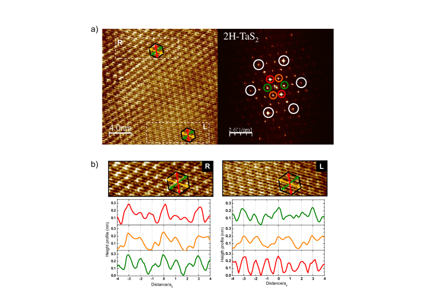
The STM topography at constant current of 2H-TaS2 taken at 100 mK is shown in Fig.1a. The hexagonal atomic S lattice is nicely observed, together with a remarkable triangular 3x3 charge modulation of wavelength 3 times the lattice constant. The Fourier transform of the whole image (right panel of Fig.1a) shows that the CDW modulation is located at one third the in-plane reciprocal lattice wavevectors, within experimental error of 1%. The CDW modulation leads to hexagons spanned by 3 vectors parallel to the three symmetry axis of the hexagonal atomic lattice, repeating itself in the topography. We identify two regions with different hexagonal patterns produced by the CDW modulation, marked by white rectangles in Fig.1. In each region, within a given hexagon, the amplitude of the charge density along the three principal CDW vectors has an angular dependence, breaking six-fold rotational symmetry. The amplitude relationship between the three modulations varies when going from the upper left corner to the lower right corner. In Fig.1b we show representative topography profiles along the three CDW wavevectors. The CDW amplitude is highest along the red arrow direction in the upper left corner, and along the green arrow direction in the lower right corner. The hexagonal pattern spanning the CDW modulation, changes as a function of the position in the image, without any step or impurity cutting the image in two. Note that both parts cannot be transferred into each other by a simple rotation.
The angular dependence of the CDW modulation observed in the real space can be further characterized by making a detailed Fourier analysis. If we look at the Fourier transforms of the two different areas marked by rectangles in Fig.1a, we find that the amplitude of CDW Bragg peaks decrease clockwise (in R) and counter-clockwise (in L), respectively. The normalized amplitude relationships for, respectively, (red), (orange), and (green), are 1-0.6-0.4 for the upper part of the image (R in Fig.2b), and 0.6-0.8-1 for the bottom part of the image (L in Fig.2b). This behavior is not followed by the intensity changes of the lattice Bragg peaks and evidences the presence of chiral domains in the CDW of 2H-TaS2.
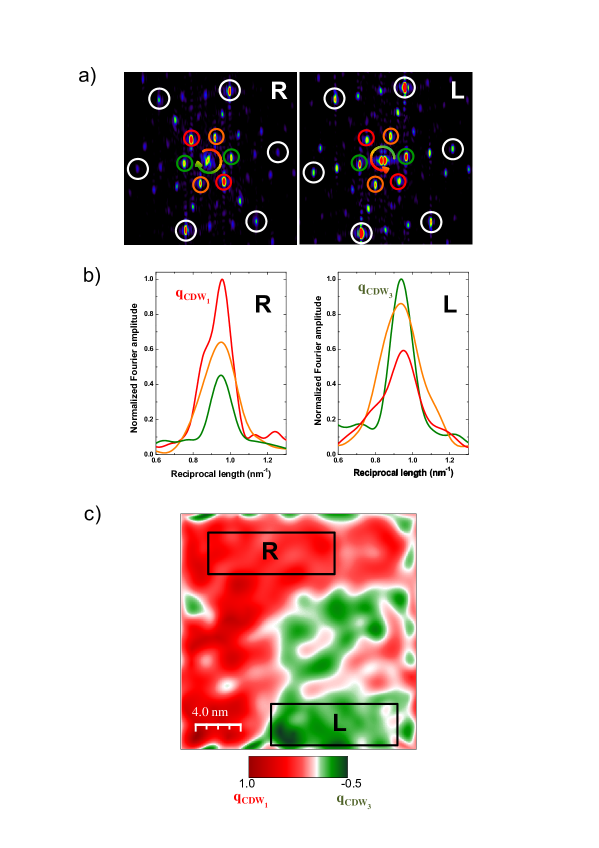
The spatial distribution of the chiral domains can be imaged by further Fourier analysis. We first Fourier transform the whole real space image (shown in Fig.1a), center the resulting Fourier image at the peak corresponding to CDW’s component with highest amplitude in the upper left corner domain (q), filter the rest of the image out, and re-transform into real space. This gives us the real space dependence of the CDW amplitude corresponding to the wavevector q. We then make the same procedure for the CDW modulation corresponding to q which has the highest amplitude in the lower right corner domain. Finally, we subtract both imagesZeljkovic11 obtaining the map of the relative height between both modulations (Fig.2c). We use red color for the area where q has highest amplitude, and green color for the area where q has highest amplitude (Fig.2c). White color is used for the boundary, where both modulations have equal amplitude. The size of the areas with different CDW modulations is rather large, of up to 10 nm, and their boundary is irregular.
The height of the atomic and CDW Fourier Bragg peaks measured in the transition metal di-chalcogenides depends always on the direction. This is the result of the complex Moiré-pattern, with very different hexagonal symmetry structures appearing in different positions, ubiquitously observed in these materials (see e.g. Coleman88 ; Giambattista88 ). Calculating precisely the local density of states to obtain such patterns is a problem of great complexity. Tip-sample coupling, depending on the detailed band structure of the sample, and of the form and geometry of the tip, or defects, shape considerably the measured local density of states Tersoff83 ; Guillamon08PRB . For example, Moiré patterns of 2H-NbSe2 have been widely discussed in literature, and related to different tip-sample coupling effects. In 2H-TaS2, within the same image, without any change in the properties of the tip nor of the surface (i.e. without any step, defect, or surface anomaly), the Moiré patterns change its symmetry properties, in a rather complex way, as shown in Figs. 1 and 2. This was first found in 1T-TiSe2 Ishioka10 , and, to the best of our knowledge, was never observed previously in any metallic 2H dichalcogenide compound. To explain such patterns, it is needed to consider out-of-plane decoupling of the three components of the CDW, which are combined in two different ways in different areas of the surface, giving chiral CDW orderIshioka10 .
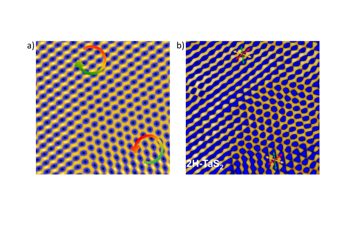
Microscopic origin of chiral charge arrangements is now under debate. Electronic interactions between planes (along c), which separate in-plane charge modulations through Coulomb interaction, can lead to a c-axis chiral modulation of the CDWIshioka10 . More recently, it has been shown that chiral charge order can also appear in relation to orbital order, which produces transversal polarization introducing phase shifts in the CDW Jasper11 . The charge modulation observed in 2H-TaS2 can be simulated by assuming that the intensity of the modulations corresponding to each changes as a function of the out-of-plane stacking, or by phase shifting each component Ishioka10 ; Jasper11 . For example, if we sum up three CDW components with r) r (with Ai the amplitude of ), and two different amplitude relationships in two different areas, we obtain the image shown in Fig.3a. Qualitatively, the obtained shapes agree with the experimental image of the CDW (Fig.3b).
All these observations, which are similar to those reported in the compound 1T-TiSe2Ishioka10 , demonstrate that 2H-TaS2 has a chiral modulation of its CDW. Note that 2H-TaS2 is a metal which superconducts, but 1T-TiSe2 is a semimetal, with no report of superconducting correlations at ambient pressureKusmartseva09 . Note also that in 1T-TiSe2 the CDW modulation is located at two times the lattice constant, whereas in 2H-TaS2 it is located at three times the lattice constant. The three fold in-plane symmetry with clockwise and counterclockwise domains appearing in the charge order features, are, however, similar. Furthermore, in 1T-TiSe2, there is a c-axis modulation of the CDW Ishioka10 , with periodicity 2 times the c-axis lattice constant. In 2H-TaSe2, interlayer separation is highest among the 2H series (it is continuously decreasing from 2H-TaSe2, 2H-TaS2, 2H-NbSe2 and is smallest in 2H-NbS2 where no CDW is observed) the three coexisting CDWs lead to a reduction of the crystal symmetry from hexagonal to orthorhombic Littlewood82 . In 2H-NbSe2, as discussed above, no chiral CDW has been reported, in spite of having been very extensively studied by many different groups. It could be that 2H-TaS2 lies in between both cases, being sufficiently 2D to present de-coupling of CDW modulations, but not enough to show structural transition or to destroy superconductivity through a too strong destruction of the Fermi surface by the CDW gap opening.
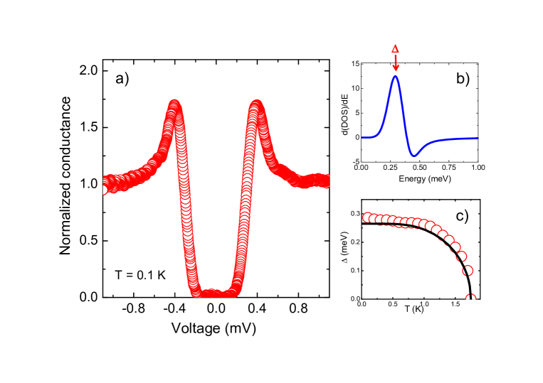
The superconducting tunneling conductance of 2H-TaS2 measured at 100 mK is shown in Fig.4. The tunneling conductance remains flat until around 0.15 mV, where it starts increasing continuously until 0.4 mV, where the quasiparticle peak is located. Such a feature is found over large parts of the surface, and we could not, until now, observe changes related to the domains of the chiral CDW modulation. The behavior is instead reminiscent of the compounds 2H-NbSe2 and 2H-NbS2, where a distribution of values of the superconducting gap, starting also roughly at half the maximal gap value, is found. In the latter compounds, however, two clear features are seen in the tunneling conductance, which show up as two peaks in the derivative of the corresponding density of statesGuillamon08 ; Rodrigo04c . These features are due to the two band superconducting properties characteristic of these compounds. Here, the derivative of the density of states (DOS, obtained by de-convoluting the temperature, as shown in Ref.Guillamon08 ), shows only one broad peak centered at =0.28 meV (Fig.4), which evolves until the Tc=1.75 K following roughly BCS theory. The value we find for is close to, although somewhat larger, than the value expected within BCS theory, =1.76kBTc=0.265 meV. Thus, the superconducting gap of 2H-TaS2 has a significant anisotropy, and the two gap features characteristic of 2H-NbSe2 and 2H-NbS2 are, if they exist at all, less clearly resolved in the superconducting density of states.
Our results establish that, in 2H-TaS2, chiral CDW properties coexist with superconductivity. Possible consequences could be related to those found in the context of other superconductors with broken space inversion symmetry. For example, in a superconductor with broken space parity and strong spin orbit coupling (spin orbit coupling is strong in 2H-TaS2 as discussed in Ref.Rossnagel07 ), the two fold electronic spin degeneracy may be lifted, and spin structured Cooper pairs could appear Edelstein95 ; Schnyder10 ; Bauer10 ; Gorkov01 ; Samokhin08 . The form and size of the superconducting gap can be under such conditions peculiar, with nodes along some directions, but it can be also fully opened Suderow09 ; Mackenzie03 . In 2H-TaS2, the observation of an opened somewhat anisotropic gap, similar to the ones found in related materials, shows that the influence of broken space parity in the superconducting properties is, if present, weak. Characterization of superconductivity in the other system of the series, 2H-TaSe2Rossnagel07 , the observation of the vortex lattice in both compounds, and a closer look to superconductivity in related CDW materials, should bring further advance.
In summary, we have observed a chiral CDW in a metallic and superconducting compound, 2H-TaS2, and provide measurements of its superconducting density of states. We could not establish an influence of broken space parity through a helical electronic structure on the superconducting density of states, but the mere presence of both phenomena in the same material, calls for more work in this and similar compounds.
We acknowledge discussions with P. Kulkarni, K. Machida, A.I. Buzdin, J. Flouquet and F. Guinea. The Laboratorio de Bajas Temperaturas is associated to the ICMM of the CSIC. This work was supported by the Spanish MICINN (Consolider Ingenio Molecular Nanoscience CSD2007-00010 program and FIS2008-00454 and by ACI-2009-0905), by the Comunidad de Madrid through program Nanobiomagnet, and by NES program of the ESF.
References
References
- (1) P.W. Anderson and E.I. Blount. Symmetry considerations on martensitic transformations: ”Ferroelectric” metals ? Phys. Rev. Lett., 14:217, 1965.
- (2) T. Kiss, T. Yokoya, Aa. Chainany, S. Shin, T. Hanaguri, M. Nohara, and H. Takagi. Charge-order-maximized momentum-dependent superconductivity. Nature Physics, page 12 August issue, 2007.
- (3) K. Rossnagel, O. Seifarth, L. Kipp, M. Skibowski, D. Voß, P. Krüger, A. Mazur, and J. Pollmann. Fermi surface of and its implications on the charge-density-wave mechanism. Phys. Rev. B, 64:235119, 2001.
- (4) A. H. Castro Neto. Charge density wave, superconductivity, and anomalous metallic behavior in 2d transition metal dichalcogenides. Phys. Rev. Lett., 86:4382 – 4385, 2001.
- (5) H. Suderow, V.G. Tissen, J.P. Brison, J.L. Martinez, and S. Vieira. Pressure induced effects on the Fermi surface of superconducting 2H-NbSe2. Phys. Rev. Lett., 95:117006, 2005.
- (6) H. F. Hess, R. B. Robinson, and J. V. Waszczak. Vortex-core structure observed with a scanning tunneling microscope. Phys. Rev. Lett., 64:2711, 1990.
- (7) F. Gygi and M. Schluter. Angular band structure of a vortex line in a type-II superconductor. Phys. Rev. Lett., 65:1820, 1990.
- (8) N. Hayashi, M. Ichioka, and K. Machida. Star-shaped local density of states around vortices in a type-II superconductor. Phys. Rev. Lett., 77:4074, 1996.
- (9) I. Guillamon, H. Suderow, S. Vieira, L. Cario, P. Diener, and P. Rodiere. Superconducting density of states and vortex cores of . Phys. Rev. Lett., 101:166407, 2008.
- (10) J. A. Wilson, F. J. DiSalvo, and S. Mahajan. Charge-density waves and superlattices in the metallic layered transition metal dichalcogenides. Adv. Phys., 24:117, 1975.
- (11) R. Corcoran, P. Meeson, Y. Onuki, P.A. Probst, M. Springford, K. Takita, H. Harima, G.Y. Guo, and B.L. Gyoffry. Quantum oscillations in the mixed state of the type II superconductor 2H-NbSe2. J. Phys. Cond. Matt., 6:4479 – 4492, 1994.
- (12) M. D. Johannes, I. I. Mazin, and C. A. Howells. Fermi-surface nesting and the origin of the charge-density wave in NbSe2. Phys. Rev. B, 73:205102, 2006.
- (13) Y. Ge and A.Y. Liu. Physical Review B, 82:155133, 2010.
- (14) W. Sacks, D. Roditchev, and J. Klein. Voltage-dependent STM image of a charge density wave. Phys. Rev. B, 57:13118 – 13131, 1998.
- (15) E. Boaknin, M. A. Tanatar, J. Paglione, D. Hawthorn, F. Ronning, R. W. Hill, M. Sutherland, L. Taillefer, J. Sonier, S. M. Hayden, and J. W. Brill. Heat conduction in the vortex state of NbSe2: Evidence for multiband superconductivity. Phy. Rev. Lett., 90:117003, 2003.
- (16) J. G. Rodrigo and S. Vieira. STM study of multiband superconductivity in NbSe2 using a superconducting tip. Physica C, 404:306, 2004.
- (17) J. D. Fletcher, A. Carrington, P. Diener, P. Rodiére, J.P. Brison, R. Prozorov, T. Olheiser, and R. W. Giannetta. Penetration depth study of superconducting gap structure of 2H-NbSe2. Phys. Rev. Lett., 98:057003, 2007.
- (18) Y. Noat, T. Cren, F. Debontridder, D. Roditchev, W. Sacks, P. Toulemonde, and A. San Miguel. Signatures of multigap superconductivity in tunneling spectroscopy. Phys. Rev. B, 82:014531, 2010.
- (19) J. Kacmarcik, Z. Prbulova, C. Marcenat, T. Klein, P. Rodiere, L. Cario, and P. Samuely. Specific heat measurements of a superconduting single crystal in an external magnetic field: energy gap structure. Phys. Rev. B, 82:014518, 2010.
- (20) L.N. Bulaevskii. Superconductivity and electronic properties of layered compounds. Sov. Phys..-Usp., 18:514, 1976.
- (21) F.J. DiSalvo, D.E. Moncton, and J.V. Waszcak. Electronic properties and superlattice formation in the semimetal TiSe2. Phys. Rev. B, 14:4321, 1976.
- (22) J. Ishioka, Y.H. Liu, K. Shimatake, T. Kurosawa, K. Ichimura, Y. Toda, M. Oda, and S. Tanda. Chiral charge-density waves. Phys. Rev. Lett., 105:176401, 2010.
- (23) A. P. Mackenzie and Y. Maeno. The superconductivity of and the physics of spin-triplet pairing. Rev. Mod. Phys., 75:657, 2003.
- (24) J. G. Rodrigo, H. Suderow, S. Vieira, E. Bascones, and F. Guinea. Superconducting nanostructures fabricated with the scanning tunnelling microscope. J. Phys.: Condens. Matter, 16:1151, 2004.
- (25) H. Suderow, I. Guillamon, and S. Vieira. Compact very low temperature scanning tunneling microscope with mechanically driven horizontal linear positioning stage. Rev. of Sci. Inst., 82:033711, 2011.
- (26) I. Zelkjovic, E.J. Main, T.L. Williams, M.C. Boyer, K. Chatterjee, W.D. Wise, T. Kondo, T. Takeuchi, H. Ikuta, G.D. Gu, E.W. Hudson, and J.E. Hoffman. STM imaging of inversion-symmetry-breaking structural distortion in the Bi-based cuprate superconductors. ArXiv, page 1104.4342, 2011.
- (27) R. V. Coleman, B. Giambattista, P. K. Hansma, A. Johnson, W. W. McNairy, and C. G. Slough. Scanning tunneling microscopy of charge density waves in transition metal chalcogenides. Advances in Physics, 37:559–644, 1988.
- (28) B. Giambattista, A. Johnson, R. V. Coleman, B. Drake, and P. K. Hansma. Scanning tunneling microscopy of charge density waves in transition metal chalcogenides. Phys. Rev. B, 37:2741, 1988.
- (29) J. Tersoff and D. R. Hamann. Theory and application for the scanning tunneling microscope. Phys. Rev. Lett., 50, 1998.
- (30) I. Guillamon, H. Suderow, F. Guinea, and S. Vieira. Intrinsic atomic-scale modulations of the superconducting gap of 2H-NbSe2. Phys. Rev. B, 77:134505, 2008.
- (31) J. van Wezel. Chirality and orbital order in charge density waves. ArXiV, 1106.1930v1.
- (32) A.F. Kusmartseva, B. Sipos, H. Berger, L. Forro, and E. Tutis. Pressure induced superconductivity in pristine 1T-TiSe2 Phys. Rev. Lett., 103:236401, 2009.
- (33) P.B. Littlewood and T.M. Rice. Theory of the splitting of discommensurations in the charge-density-wave state of 2H-TaS2. Phys. Rev. Lett., 48:27, 1982.
- (34) K. Rossnagel and N.V. Smith. Spin-orbit splitting, Fermi-surface topology, and charge-density-wave gapping of 2H-TaSe2. Phys. Rev. B, 76:073102, 2007.
- (35) V.M. Edelstein. Magnetoelectric effect in polar superconductors. Phys. Rev. Lett., 75:2004, 1995.
- (36) A.P. Schnyder and S. Ryul. Topological phases and flat surface bands in superconductors without inversion symmetry. arXiV:1011.1438v1, 2010.
- (37) E. Bauer, G. Rogl, X.Q. Chen, R.T. Khan, H. Michor, G. Hilscher, E. Royanian, K. Kumagai, D.Z. Li, Y.Y. Li, R. Podloucky, and P. Rogl. Unvoncentional superconductivity in weakly correlated, non-centrosymmetric Mo3Al2C. arXiV:107.0420v1, 2010.
- (38) L.P. Gor’kov and E.I. Rashba. Superconducting 2D system with lifted spin degeneracy: Mixed singlet-triplet state. Phys. Rev. Lett., 87:037004, 2001.
- (39) K.V. Samokhin and V.P. Mineev. Gap structure in noncentrosymmetric superconductors. Phys. Rev. B, 77:104520, 2008.
- (40) H. Suderow, V. Crespo, I. Guillamon, S. Vieira, F. Servant, P. Lejay, J.P. Brison, and J. Flouquet. A nodeless superconducting gap in Sr2RuO4 from tunneling spectroscopy. New Journal of Physics, 11:093004, 2009.