A New Artificial Dielectric Metamaterial and its Application as a THz Anti-Reflection Coating
Abstract
We describe a novel artificial dielectric material which has applications at millimetre and submillimetre wavelengths. The material is manufactured from layers of metal mesh patterned onto thin polypropylene sheets which are then bonded together using a hot pressing process to provide planar rugged discs which can be reliably cycled to cryogenic temperatures. The refractive index of this material can be tuned by adjusting the geometry and spacing of the metal-mesh layers. We demonstrate its usage by designing and characterising a broadband anti-reflection coating for a Z-cut crystalline Quartz plate. The coating was fabricated and applied to the quartz using the hot press technique and characterized using a Fourier Transform Spectrometer. The performance is shown to be in good agreement with HFSS and transmission line modelling results.
1 Introduction
Metal mesh technology has been adopted in the millimetre and sub-millimetre wavelength range (THz frequencies) as the standard method for fabricating optical filters, beam-splitters and dichroics [1, 2, 3, 4]. Components fabricated using this technique have been used in a number of THz cameras and spectrometers [5, 6, 7, 8, 9]. More recently, the same technique has been used to manufacture half-wave plates using aligned metallic patterns with air-gap spacing between the layers [10]. These traditional metal mesh components are not considered metamaterials because their electromagnetic properties are not independent of their thickness, i.e. they cannot be characterized as having a bulk electric permittivity and magnetic permeability.
This paper demonstrates that closely spaced multiple layers of metal-mesh films embedded in polypropylene behave as an artificial dielectric metamaterial. By changing the metal mesh geometry the effective impedance of the mesh layer is modified changing the apparent refractive index of the overall material. In Section 2 we present a theoretical analysis to obtain a physical insight into this behaviour and to show how the geometrical parameters modify the effective dielectric constant. This modelling uses a commercial finite-element analysis package: High Frequency Structure Simulator (HFSS; [11]), which provides an exact solution to Maxwell′s equations for a unit cell of the structure.
As a demonstration, a prototype broadband anti-reflection coating was designed and applied to a single Z-cut quartz plate. In Section 3 spectral measurements of both the anti-reflection coating and of the quartz plate before and after coating with the artificial dielectric are presented. These results are compared with predictions from HFSS and our own transmission line model.
2 Theory and modeling
2.1 Theoretical elements
The metal mesh technology described in Ade et al. [1] is based on standard two port microwave circuit analysis. The metal mesh layer is modelled as an equivalent lumped LC filter and the spacing between meshes is modelled as a transmission line with impedance, where is the impedance of free space and is the index of refraction of the material between meshes. The lumped element impedance for a single sheet containing periodic metal structures has been previously determined by a number of authors [12, 13, 14, 15] to be dependent only on the geometric properties of the metal.
For filters and other components built up of many individual metal meshes, the metallized layers are stacked together with plane parallel spacers, which consist of either air gaps or dielectric discs. The model is successful in designing and predicting the performance when the spacing between layers , is large enough so that there is relatively little inductive or capacitive coupling between layers. Air gap devices require an annular support ring, while the dielectric spacers and metallized sheets can be fused together using a hot pressing technique to make a solid self-supporting disc. While the design of these components is based on radiation at normal incidence to the metal mesh layers, their performance, which is measured in a converging beam of half angle 9.6 degrees (see later), agree well. This indicates that there is not a strong dependence with off-axis angle.
The simplest metal mesh pattern used for low pass filters is termed a capacitive grid as described in Ade et al. [1]. Here we describe the properties of a stack of identical capacitive mesh grids with spacing between the grids, immersed in a dielectric substrate layer using hot-pressed technology. In these structures, the two port microwave circuit model breaks down due to the capacitive coupling between layers. However, the properties of the components are well described by an effective bulk permittivity, and bulk permeability, corresponding to a material with effective index of refraction, . By changing the basic mesh geometry, the mesh layer spacing and the number of mesh layers the effective permittivity of the newly created artificial dielectric slab can be modified. This is expected since the lumped capacitance of the grids will increase the capacitance per unit length for an electric field parallel to grids, thus increasing the effective permittivity of the material. A full EM analysis of structures made of solid metal bars with gaps between them has been reported [16]. We perform a semi-empirical analysis of our structures based on 3-D EM simulations using HFSS and compare these results to measurements of fabricated components.
2.2 Essential parameters in the build
Figure 1 shows the basic structure of the capacitive metal mesh layers embedded in a base dielectric material such as polypropylene.
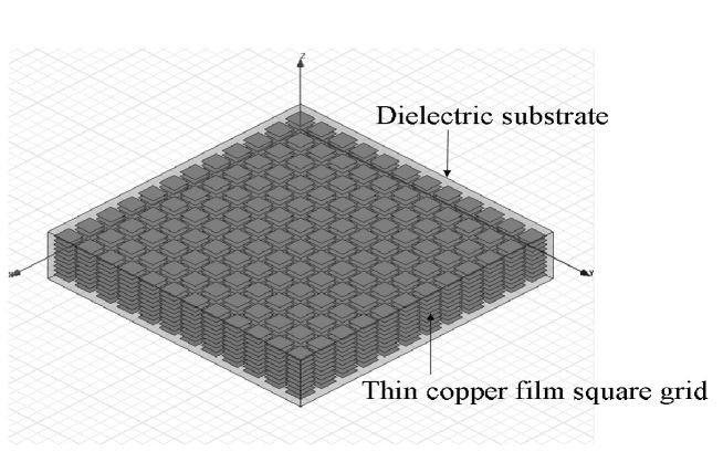
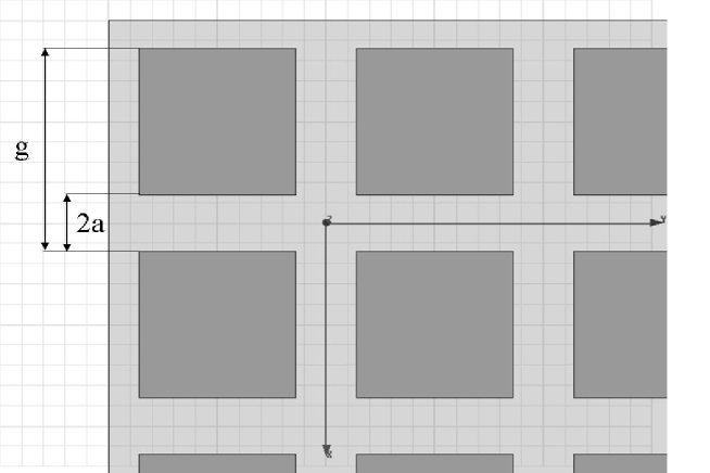
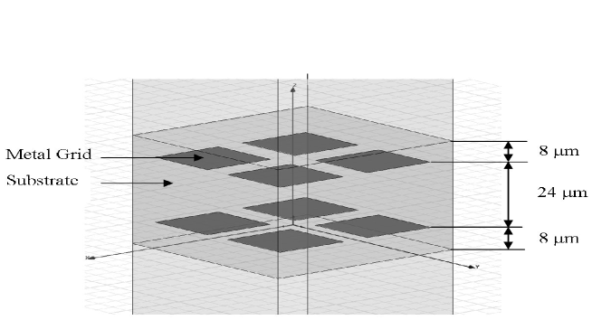
The structure of a single mesh layer is periodic so there are only three essential geometrical parameters in the model; the spacing between the layers, d, the gap between two adjacent metallic squares, 2a, and the period of the repetitive square structure, g, as shown in Figure 2. It was also found useful to categorize the mesh patterns by the ratio a/g since for a given grid period this characterizes the basic frequency dependence of the single mesh.
2.3 HFSS simulation result for metal mesh dielectric
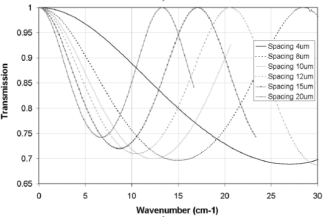
We used HFSS simulations to explore the optical properties of these capacitive grid stacks with different geometrical properties. For these simulations we fixed the basic grid periodicity, g, to be 100 m. Changing this dimension along with the spacing between the layers scales the observed properties to different spectral regions. The simulations were made for a range of a/g ratios from 0.05 up to 0.28 (0.05, 0.1, 0.14, 0.28). For each a/g, we also varied the number of layers (5, 10, 20 layers) and explored the dependence on the grid spacing, d, between adjacent layers (4, 5, 8, 10, 12, 15 and 20 m).
The simulation transmission results for one set of a ten layer device with a/g = 0.28 for various grid spacing are shown in Figure 3.
The refractive index, n, is derived from the transmission data by assuming that the resultant material behaves like a plane parallel dielectric plate with thickness, . From the HFSS simulation we obtain the complex reflection and transmission coefficients, r and t, of the material and invert the standard Fabry-Perot (FP) transmission formulas [17]:
| (1) |
and
| (2) |
to determine the index of refraction, n and material impedance, z. From these we can compute values for the relative permittivity, and permeability, . We find for all structures that independent of frequency so the material can be characterized as a simple dielectric and the index can be calculated from the FP intensity formula [18]:
| (3) |
or simply by measuring the transmitted intensity at the first minimum:
| (4) |
Inversion of this for the transmission at the first minima observed in Figure 3 gives the effective refractive index for the artificial material at that frequency.
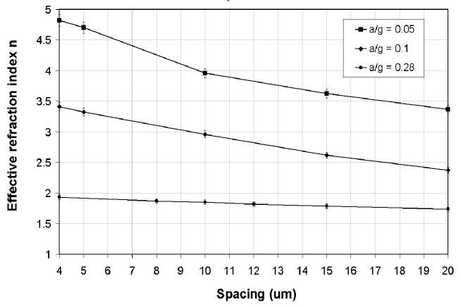
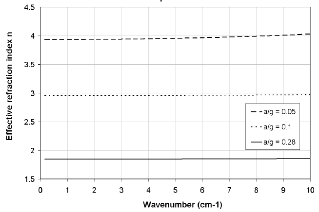
The estimated refractive index as a function of the grid spacing for each a/g ratio is presented in Figure 4. This shows that for a fixed a/g ratio, the refractive index of the material decreases as the grid spacing increases. It can also be seen that for a fixed grid spacing, a higher a/g ratio yields a lower refractive index. For both cases an increase in the grid spacing or the a/g ratio results in a decrease per unit length of the effective artificial material capacitance for an E-field parallel to grids and hence a decrease in refractive index. We perform simulations of structures with different numbers of mesh layers and find that the effective index of refraction is independent of component thickness and therefore can be considered a bulk material parameter. Finally, Figure 5 shows that the index of refraction is weakly dependent on the frequency and that the metamaterial behaves as an artificial dielectric over a wide range of wavelengths, corresponding to .
2.4 HFSS model parameters for anti-reflection coating
One important application of this artificial dielectric is as an element in a broadband multilayer anti-reflection coating (ARCs). In this application there are two fundamental material requirements that need to be met. First, the materials used in ARCs must have a range of appropriate refractive indices and high transparency over the desired spectral band. Secondly, the material must be mechanically suitable for applying to crystalline materials.
ARCs are usually used to maximize the device transmission over spectral bandwidths approaching 100 %. Previous designs used specially prepared polypropylene layers[19, 20] that are loaded with high refractive index powders (TiO2) or ceramic based materials (e.g., Rogers TMM material [21]) to create a particular refractive index. These ARCs needed three layers to achieve a flat response across the band. Each layer required hot pressing or grinding to the required thickness before being bonded to the front and back surfaces of the crystalline plates [19, 22]. Major problems were encountered with both the previous approaches. The loaded powder layers were slow to manufacture since the powder needed to be uniformly mixed in the polypropylene and then the layers had to be hot pressed to the appropriate thickness. The ceramics are brittle and could only be thinned by using a grinding technique which proved to be time consuming and difficult to handle in thin sheet form.
Compared with the previous techniques, the artificial dielectric design has the advantages of simple refractive index tuning through the geometry and spacing of the grids. Without high index powders added into the material, the metal mesh design has a complete control over the thickness of the coating layer and the coating material is not brittle and has better performance in thermal cycling. Furthermore, since the base dielectric is polypropylene, it also has low absorption for frequencies up to 20 THz [23]. Thus the artificial dielectric meets with the ARC fundamental requirements.
To demonstrate the new material we have prototyped an ARC for a Z-cut crystal quartz plate with refractive index n=2.1. To increase the spectral bandwidth of the low reflection region we needed two materials with intermediate refractive index values close to 1.3 and 1.7. The first of these is realised using readily available porous PTFE whilst the latter requires the customised artificial dielectric.
The artificial dielectric is constituted by two essential elements, a metal mesh grid and the embedding dielectric. The first is obtained by photo-lithographic techniques adopted in the manufacturing of far-infrared low-pass filters [24]. The copper deposited patterns on thin substrates (8 m) of polypropylene are then inserted into a stack (see Figure 6). The two metal mesh layers were immersed in the substrate at a distance of 8 m from the top and bottom surfaces and with a spacing s=24 m between two layers. The single mesh layers are periodic structures of square grids patterns. In this design with g=25.4 m and a=3.556 m. Once the 40 m multi-layer structure is assembled it is then fused by hot-pressing the layers at high temperature near the polypropylene melting point (160∘ C). The temperature is such that the polypropylene layers are joined but is insufficient to allow the polymer chains to flow in a liquid-like manner. Expansion due to relaxation when hot pressing the layers is avoided by maintaining high pressure in the press and through the absence of soft materials in the stack. Thicknesses measurements made after hot pressing show that the layer thicknesses are maintained to better than m.
The artificial material created by this process has the consistency of a solid plastic film which can be easily handled and cut to size to suit requirements. Bonding of this material to the quartz crystal is again performed through a cycle of thermal heating with applied pressure using a thin layer of polymer based glue (thickness wavelength). Finally, the outer layers of porous PTFE are again glued at the extremes of the stack (top layer in Figure 7)with identical procedure (the two procedures can in fact be performed in one single press cycle).
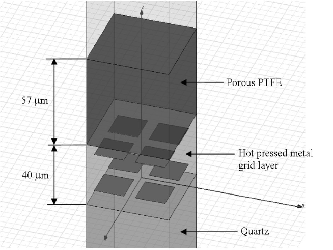
The ARC layers are symmetrical with respect to the central crystal in order to taper the impedance that a given wavelength of radiation experiences when entering and subsequently exiting the crystal.
2.5 HFSS prediction for anti-reflection coating
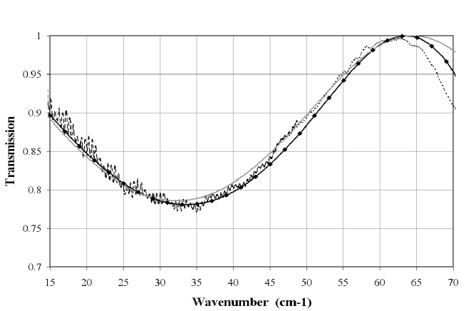
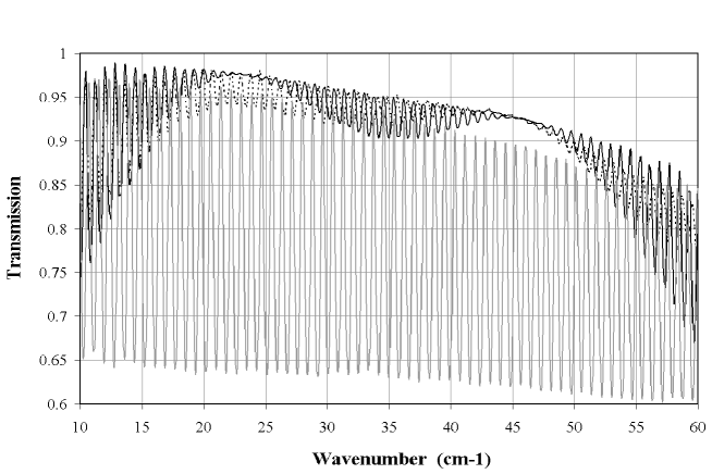
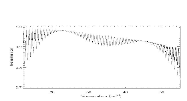
Simulations for both the prototype ARC on its own and the completed quartz plate with AR coatings have been made. The transmission for the prototype ARC layer is shown in Figure 8. The refractive index was calculated based on transmission as described in section 2.3 to be 1.65 in average. Figure 9 shows the comparison between the uncoated quartz substrate, the AR-coated substrate and the simulated transmission expected. The efficiency of the coating yielding high transmission over the frequency band from 18.6–52 cm-1 (560–1560 GHz) is obvious.
3 Measurements and Data Analysis
As a stand-alone material, the embedded grids in polypropylene will have a complex impedance with the real part mimicking a behaviour analogous to that of a plane parallel dielectric slab. We therefore subjected the material to the same spectral tests that we would have imposed on a thin dielectric slab to determine its refractive and absorptive properties.
The material has also been measured when used as a tuned anti-reflection coating element. As reported above for this measurement it was hot pressed on both sides of a quartz plate. We were careful to choose grids with a period of 25.4 m to ensure that diffraction effects would be negligible at the frequencies for which the ARC was optimised. However, we expected to observe spectral features resulting from the complex impedance nature of the resonant structures which would distinguish the measured spectral behaviour from that of a normal dielectric with constant index of refraction.
3.1 Spectral measurements of the material.
To verify the optical properties of the artificial dielectric alone and with the crystal, we placed the material in the f/3 beam of a rapid scanning polarizing Fourier Transform Spectrometer (FTS). The spectral features associated with the source (a Hg-arc lamp) together with the spectral efficiency of the detector (a 4 Kelvin Ge bolometer) were removed by performing the ratio with a background spectrum recorded with the sample removed. Three sets of 10 scans each were performed in order to obtain acceptable signal to noise for a spectral resolution of 0.25 cm-1 and limit phase errors in the Fourier transform process. Interferograms in each set were averaged and then Fourier Transformed. The resulting three spectra have then been averaged before ratioing against the background spectrum. The final transmission spectrum is shown in Figure 8. By repeating this measurement at various orientation of the mesh axises with respect to the polarization direction we confirmed there is no polarization sensitivity observable above 1 % level as expected.
From the peak of transmission at 62 cm-1 we can infer that absorption loss due to the polypropylene, which is usually a monotonic function of frequency, is negligible. Data for the absorption coefficient of Tucker and Ade [23] indicate that the expected loss would be only 0.2 %. With this consideration we can expect the transmission of an equivalent dielectric slab to be given by equation (1). By inverting this equation whilst fixing the physical thickness of the material we can numerically solve for each value of to obtain a value . Figure 10 shows the residual mismatch of the FTS data with the ideal Fabry-Perot behaviour. The contour levels are the percentage error on the transmission mismatch (measured/ideal). The thick line in the clear contour region shows the best fit over the spectral interval 20–40 cm-1 for an assumed linear function of frequency. The linear fit parameters are:
| n | (5) | ||||
| (6) | |||||
| (7) |
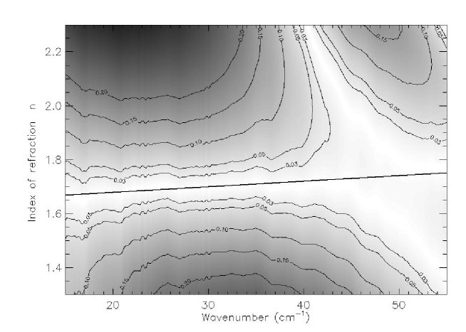
The small ripple artifacts which are visible in the leftmost region of the contour, arise from standing waves in the FTS sample box between the sample and the output polariser, and hence have been ignored in the fitting procedure.
Using these values as initial conditions for a simulation of the complete stack we can then proceed to verify that its employment as an anti-reflection coating element is consistent with its stand-alone properties.
3.2 Spectral measurements of coated quartz substrate.
As previously stated, the end goal is to produce a broadband anti-reflection coating to remove reflection loss from high refractive index crystalline components. The complete ARC structure as described above was measured in the identical setup as the stand-alone material. Figure 9 presents these data which can now be compared with the spectral performance as simulated at a number of frequencies using HFSS.
First, we note that in general there is good agreement between the envelopes of the fringes. This denotes that the material is acting as a good anti-reflection coating over the desired band. However, some minor discrepancies are also present which question either the set of input parameters for the simulation or our understanding of the effects.
Having manufactured a large number of anti-reflection coated windows and filters with different techniques, we are aware that some of the parameters can slightly change due to the heat-bonding process in our press. Indeed some bonding materials change when heated. Porous PTFE can be pressed to a smaller thickness and being porous can absorb some of the polyethylene glue, raising the equivalent index of refraction by a small amount and changing its final thickness. Polypropylene on the other hand tends to relax and expand if there is not sufficient pressure placed on it. Crystals clearly will not be deformed at these temperatures and pressures.
Performing HFSS simulations with different values of parameters at multiple frequencies proves to be very time consuming, so we have adopted a transmission line based model [22] to perform a Monte-Carlo simulation cycling through some of the input parameters (thickness of the coating layers and indexes of refraction to find the solution which closely matches our data set and check for potential manufacturing effects.
In order to justify the results we first tested the consistency of the two simulation/modelling packages by running the transmission line model on the nominal input-parameters. In Figure 11 we can clearly see an excellent agreement from low to high-frequencies with the two best-matching regions in 20–25 and 42–46 cm-1. The loss of relative precision in the HFSS simulation at the higher frequencies is potentially the cause of the mismatch occurring there.
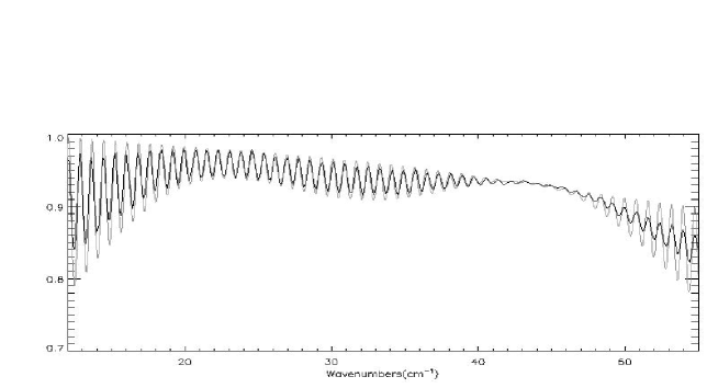
The Monte-Carlo parameter fit results and minimum square residuals are given in Table 1 for the best fit of the data shown in Figure 12. This fit, performed over the region 15–55 cm-1, yields a good match with the following caveats regarding the numbers in Table 1:
-
•
Mupor [25]: Porous PTFE. The increase in the mupor index and its decrease in average thickness is consistent with compression of a porous material during bonding.
-
•
ADM - t: The thickness of the Artificial Dielectric Material (ADM). The values of thickness slightly larger than expected could point to thermal relaxation of the polypropylene layers. This phenomenon has been observed in direct coating of quartz windows. This tendency of thin layers to shrink in diameter and grow in thickness of a few percent can occur when the pressure applied is not sufficient or other less dense materials in the stack give way.
-
•
ADM - n: The refractive index of the Artificial Dielectric Material (ADM). The values of index of refraction are slightly different from the recovered functional values found previously ( and ) but it is important to note that in the interval of frequencies considered, the two functional dependencies are not too dissimilar.
-
•
Top-bottom asymmetry : Generally we would not expect a marked asymmetry between top and bottom coating layer thicknesses. However, we note that in the vacuum oven the top plate of the press is only conductively heated through the stainless steel press screws. A temperature difference of a few degrees will affect the tendency of materials to change their thickness subject to pressure.
-
•
Quartz n : The values of quartz index obtained are slightly different (smaller) than those in literature [26] by a scaling factor . This is expected as the standing wave pattern in the fitted data does not vary with a constant product of and the quartz thickness. To avoid additional standing waves in the measuring setup, the sample was tilted by and this would affect the thickness travelled by with . By forcing the nominal thickness the fitted value of the index of refraction compensates accordingly.
List of parameters (fixed and variable) in the simulation of the coated stack. It is important to specify that due to the nature of the fit and the different parameter intervals, the errors reported are only indicative of the dependence of the result from that parameter (i.e. how much does that variable influence the result) and not a simple standard deviation of a gaussian distribution. The two errors are respectively indicating an increase of (1)=10 % and (2)= 100% in the residual of the least square quadratic fit when applied to the specific parameter. The quartz value was measured on the substrate with a precision micrometer and the error resulting in the repeatability of the measurement across the sample.
| Parameter | Value | Error | Error | Units | |
|---|---|---|---|---|---|
| Mu-por Index of Refraction | |||||
| Mu-por Thickness (Top) | (m) | ||||
| Mu-por Thickness (Bottom) | (m) | ||||
| ADM Index of Refraction | |||||
| ADM Index of Refraction | |||||
| ADM Thickness (Top) | (m) | ||||
| ADM Thickness (Bottom) | 45 | (m) | |||
| Quartz Index of Refraction | |||||
| Quartz Index of Refraction | |||||
| Quartz Index of Refraction | |||||
| Quartz Loss Tangent | |||||
| Quartz Loss Tangent | |||||
| Quartz Thickness (*) | (fixed) |
4 Conclusions
We have shown through modelling and experimental verification that artificial dielectrics with refractive indexes above that of the base material can be obtained over a broad spectral band by fusing in layers of metal mesh. The resultant refractive index can be easily controlled by adjusting the geometrical parameters of the meshes and the spacing between them in the new material.
We have also demonstrated the viability of this metamaterial as an element in producing a broad band anti-reflection coating for a quartz crystal. Again modelling and measurement results are in good agreement showing that we have good control of this process. As a further test of the robustness of the coated layers we dropped the sample into liquid nitrogen (77K) and warmed to room temperatures five times with no discernable signs of the coating peeling of fracturing.
We believe that this new approach will assist in the manufacture of many other optical components in the FIR to millimetre wavelength range. These include flat lenses, birefringent components for waveplates (using 1-D grid structures) and dispersive components.
References
- [1] Ade P.A.R., Pisano G., Tucker C., Weaver S., “A Review of Metal Mesh Filters”, Proceedings of the SPIE, Vol. 6275, 62750U (2006).
- [2] Ulrich R., “Interference Filters for The Far Infrared”, Applied Optics, Vol. 7 , No. 10, October 1968.
- [3] Kuznetsov S.A., Kubarev V.V., Kalinin P.V., Goldenberg B.G., Eliseev V.V., Petrova E.V., and Vinokurov N.A., “Development of Metal Mesh Based Quasi-Optical Selective Components and Their Applications in High-Power Experiments at Novosibirsk Terahertz Fel”, Proceedings of FEL 2007, pp. 89–92, Novosibirsk, Russia, 2007.
- [4] Naylor D.A., Gom B.G., Schofield I. S., Tompkins G. J., Davis G.R., “Mach-Zehnder Fourier Transform Spectrometer for Astronomical Spectroscopy at Submillimeter Wavelengths”, SPIE, Millimeter and Submillimeter Detectors for Astronomy 4855, 540-551, 2003.
- [5] Lamarre, J. M.; Puget, J. L.; Bouchet, F.; Ade, P. A. R.; Benoit, A.; Bernard, J. P.; Bock, J.; de Bernardis, P.; Charra, J.; Couchot, F.; Delabrouille, J.; Efstathiou, G.; Giard, M.; Guyot, G.; Lange, A.; Maffei, B.; Murphy, A.; Pajot, F.; Piat, M.; Ristorcelli, I.; Santos, D.; Sudiwala, R.; Sygnet, J. F.; Torre, J. P.; Yurchenko, V.; Yvon, D. “The Planck High Frequency Instrument, a third generation CMB experiment, and a full sky submillimeter survey”, New Astronomy Reviews, Volume 47, Issue 11-12, p. 1017-1024, 2004.
- [6] Fowler J.W., Niemack M. D., Dicker S. R., Aboobaker A. M., Ade P. A. R., Battistelli E. S., Devlin M. J., Fisher R.P., Halpern M., Hargrave P.C., Hincks A.D.,Kaul M., Klein J., Lau J. M., Limon M., Marriage T. A., Mauskopf P.D., Page L., Staggs S.T., Swetz D. S., Switzer E. R., Thornton R. J., Tucker C. E., “Optical Design of the Atacama Cosmology Telescope and the Millimeter Bolometric Array Camera”, Applied Optics, 46, Issue 17, 3444-3454, 2007
- [7] Pascale, E.; Ade, P. A. R.; Bock, J. J.; Chapin, E. L.; Chung, J.; Devlin, M. J.; Dicker, S.; Griffin, M.; Gundersen, J. O.; Halpern, M.; Hargrave, P. C.; Hughes, D. H.; Klein, J.; MacTavish, C. J.; Marsden, G.; Martin, P. G.; Martin, T. G.; Mauskopf, P.; Netterfield, C. B.; Olmi, L.; Patanchon, G.; Rex, M.; Scott, D.; Semisch, C.; Thomas, N.; Truch, M. D. P.; Tucker, C.; Tucker, G. S.; Viero, M. P.; Wiebe, D. V., “The Balloon-borne Large Aperture Submillimeter Telescope: BLAST”, Astrophys. J., 681, Issue 1, 400-414, 2008
- [8] Griffin, M.; Ade, P.; Andr , Ph.; Baluteau, J.-P.; Bock, J.; Franceschini, A.; Gear, W.; Glenn, J.; Huang, M.; King, K.; Lellouch, E.; Naylor, D.; Oliver, S.; Olofsson, G.; Page, M.; Perez-Fournon, I.; Rowan-Robinson, M.; Saraceno, P.; Sawyer, E.; Swinyard, B.; Vigroux, L.; Wright, G.; Zavagno, A., “The SPIRE Instrument”, EAS Publications Series, 34, 33-42, 2009.
- [9] Ruhl, John; Ade, Peter A. R.; Carlstrom, John E.; Cho, Hsiao-Mei; Crawford, Thomas; Dobbs, Matt; Greer, Chris H.; Halverson, Nils w.; Holzapfel, William L.; Lanting, Trevor M.; Lee, Adrian T.; Leitch, Erik M.; Leong, Jon; Lu, Wenyang; Lueker, Martin; Mehl, Jared; Meyer, Stephan S.; Mohr, Joe J.; Padin, Steve; Plagge, T.; Pryke, Clem; Runyan, Marcus C.; Schwan, Dan; Sharp, M. K.; Spieler, Helmuth; Staniszewski, Zak; Stark, Antony A., “The South Pole Telescope”, SPIE, Volume 5498, pp. 11-29,
- [10] Pisano G., Savini G., Ade P.A.R., Haynes V., “Metal-mesh Achromatic Half-wave Plate for Use at Submillimeter Wavelengths”, Applied Optics, Vol. 47, No. 33. 20 November 2008.
- [11] http://www.ansoft.co.uk/products/hf/hfss/.
- [12] Marcuvitz N., “Waveguide Handbook”, M.I.T. Rad. Lab. Ser., McGraw-Hill, 280-290, 1951.
- [13] Compton R., Rutledge D. B., “Approximation Techniques for Planar Periodic Structures”, IEEE Transactions on Microwave Theory And Techniques, Vol. MTT-33, No.10, October 1985.
- [14] Chen C.C., “Transmission of Microwave Through Perforated Flat Plates of Finite Thickness”, IEEE Transactions on Microwave Theory And Techniques, Vol. MTT-21, No.1, January 1973.
- [15] Rubin B., “Scattering from a Periodic Array of Apertures or Plates Where the Conductors Have Arbitrary Shape, Thickness, and Resistivity”, IEEE Transactions On Antennas And Propagation, Vol. AP-34, NO.11, November 1986.
- [16] Shen J.T., Catrysse P.B., and Fan Shanhui., “Mechanism for Designing Metallic Metamaterials with a High Index Refraction”, Physical Review Letters. PRL 94, 197401, 2005.
- [17] Smith D.R., Schultz S., Markos P., and Soukoulis Markos P., “Determination of Effective Permittivity and Permeability of Metamaterials from Reflection and Transmission Coefficients”, Physical Review B, Vol. 65, 195104, 2002.
- [18] Hecht E., “Optics”, ISBN 0-321-18878-0, Addison Wesley, 1301 Sansone St., San Francisco, CA94111, 2002.
- [19] Pisano G., Savini G., Ade P.A.R., Haynes V., and Gear W. K., “Achromatic Half-Wave Plate for Submillimeter Instrumentations in Cosmic Microwave Background Astronomy: Experimental Characterization’,’ Applied Optics, Vol. 45, No. 27, September 2006.
- [20] Savini G., Ade P.A.R., House J., Pisano G., Haynes V., Bastien P., “Recovering The Frequency Dependent Modulation Function of The Achromatic Half-wave Plate for POL-2: The SCUBA-2 Polarimeter”, Applied Optics, Vol. 48, pp. 2006–2013, 2009.
- [21] Rogers Corporation supply TMM high frequency laminate materials: www.rogerscorp.com
- [22] Savini G., Pisano G., and Ade P.A.R., “Achromatic Half-Wave Plate for Submillimeter Instruments in Cosmic Microwave Background Astronomy: Modeling and Simulation”, Applied Optics, Vol. 45, No. 35, August 2006.
- [23] Tucker C. and Ade P.A.R., “Thermal filtering for large aperture cryogenic detector arrays”, Proceedings of the SPIE, Vol. 6275, pp. 62750T, 2006.
- [24] Tucker C. and Ade P.A.R., “Metal-Mesh Filters for THz Applications”, Infrared and Millimeter Waves, 2007 and the 2007 15th International Conference on Terahertz Electronics, IRMMW-THz Joint 32nd International Conference, pp. 973-975, 2007.
- [25] http://www.porex.com/porous.cfm
- [26] Russell E.E. and Bell E.E., “Measurement of the optical constants of crystal quartz in the far infrared with the asymmetric Fourier-transform method”, Journal of the Optical Society of America, vol. 57, issue 3, p.341