Zener tunneling isospin Hall effect in HgTe quantum wells and graphene multilayers
Abstract
A Zener diode is a paradigmatic device in semiconductor-based electronics that consists of a - junction where an external electric field induces a switching behavior in the current-voltage characteristics. We study Zener tunneling in HgTe quantum wells and graphene multilayers. We find that the tunneling transition probability depends asymmetrically on the parallel momentum of the carriers to the barrier. In HgTe quantum wells the asymmetry is the opposite for each spin, whereas for graphene multilayers it is the opposite for each valley degree of freedom. In both cases, a spin/valley current flowing in the perpendicular direction to the applied field is produced. We relate the origin of this Zener tunneling spin/valley Hall effect to the Berry phase acquired by the carriers when they are adiabatically reflected from the gapped region.
pacs:
61.46.-w, 73.22.-f, 73.63.-bI Introduction
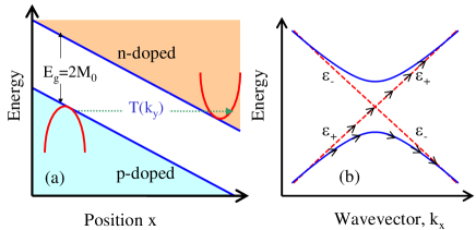
A large class of semiconductor devices is based on quantum mechanical tunneling of carriers through potential barriers. This is the case of the Zener diode, which consists of a - junction where a strong enough electric field induces interband transitions from the valence band of the -type material to the conduction band of the -doped material, see Fig. 1(a). The tunneling amplitude is highly non linear in the applied field, and the tunneling current shows a breakdown-type behavior in the current-voltage (-) characteristics. The nonlinearity of the Zener tunneling makes this device very useful for semiconductor-based electronicsSze (1981). Interband tunneling has been studied extensively in parabolic band-gap semiconductors, it is a paradigmatic example of non-adiabatic transitions, and it is known as the Landau-Zener tunnelingZener (1934); Wittig (2005). The most used model for studying the interband tunneling in parabolic semiconductors is a two-level system described by a Dirac-like Hamiltonian with a mass termKane and Blount (1969); Wittig (2005); Shevchenko et al. (2010), see Fig. 1(b). In this kind of materials, the spin of the carriers typically plays no role.
In this paper we are interested in analyzing Zener tunneling physics in systems in which there is a correlation between the carrier’s spin (or an equivalent degree of freedom) and its direction of motion, i.e., systems is which chirality plays a role. In particular, we analyze two types of materials, HgTe quantum wells and carbon-based planar heterostructures. These materials have in common that they can be described by Hamiltonians and, therefore, it is possible to map the tunneling problem to the evolution of a two-level systemShimshoni and Gefel (1991).
In the first case, HgTe quantum wells, we find that the Zener tunneling depends asymmetrically on the parallel momentum of the carriers to the barrier, and this asymmetry is the opposite for each spin. We call this phenomenon Zener tunneling spin Hall effect. In these quantum wells the central region is an inverted band-gap semiconductor, such as HgTe, whose intrinsic strong spin-orbit coupling induces an inversion of the normal band progression of typical semiconductors, like the one used for the barrier material (e.g. CdTe). This kind of materials have come to the spot-light recently because, depending on the width of the central region, the system can undergo a quantum phase transition and become a topological insulatorX.-L. Qi et al. (2006); B. Bernevig et al. (2006); M. König et al. (2007). A topological insulator is a novel quantum state of matter that has metallic surface states inside the bulk energy gap L. Fu et al. (2007); J. E. Moore etal. (2007); Murakami (2007).
In the second case, graphene multilayers, we find that the Zener tunneling is also asymmetric with respect to the parallel momentum (except for monolayer), but the asymmetry changes for each carrier’s valley index (instead of real spin). We call this phenomenon Zener tunneling valley Hall effect. Graphitic systems are also of great interest in condensed matter physics since it became possible to isolate monolayers, bilayers and in general multilayers of grapheneNovoselov et al. (2004, 2005); Zhang et al. (2005). - junctions of graphene have been created by gating locally these layers and the transport properties of these heterostructures have been studied theoretically and experimentallyKatsnelson et al. (2006); Cheianov and Fal’ko (2006); Williams et al. (2007); Zhang and Fogler (2008); Young and Kim (2009); Vandecasteele et al. (2010); Stander et al. (2009); Jena et al. (2008); Chiu et al. (2010); Brey and Fertig (2009); Arovas et al. (2010). In particular, in bilayer graphene it is possible to open a gap in the spectrum by applying a voltage difference between the layers, and Zener tunneling is expected to occur. Actually, it has recently been predicted that the - characteristics in bilayer graphene p-n junctions present, on top of the nonlinear Zener signal, some N-shaped branches with negative differential conductivityNandkishore and Levitov (2011).
In both type of materials, the low-energy Hamiltonian can be expressed in terms of a pseudospin vector that multiplies the vector of Pauli matrices. In a tunneling process, the pseudospin vector undergoes a certain trajectory in the Bloch sphere and the carrier’s wave function may acquire a Berry phase. We relate the Zener transition asymmetry with the spin/valley-dependent Berry phase that the carriers acquire when they are adiabatically reflected from the gapped region.
The paper is organized in the following way: In Section II we define the Hamiltonians that govern the properties of HgTe quantum wells and graphene multilayers. In Section III we map the tunneling problem to the time evolution of a two-level system and show numerical results for the different Hamiltonians. In Section IV we derive analytical expressions for the tunneling transition in the sudden and adiabatic approximations. In Section V the asymmetry of the tunneling amplitude as function of the momentum parallel to the barrier is explained in terms of the Berry phases that the carriers acquire upon reflection from the barrier. In Section VI we show the - characteristic curves for HgTe quantum well and multilayer graphene Zener diodes. We finish the paper in Section VII with a summary of our results.
II Hamiltonians
II.1 HgTe quantum wells
We study a HgTe quantum well confined by CdTe barriers. In bulk, and due to the strong spin-orbit coupling, HgTe is a zero gap semiconductor. When confined, HgTe is a normal band insulator for well thickness narrower than 63 and becomes a topological insulator for larger widthsM. König et al. (2007). For HgTe quantum wells grown in the (100) direction, the -component of the spin is conserved. Near the band gap there are four relevant bands: the E1 bands that consist of the two spin states of the -orbital, and the two spin states of the HH1 bands which are a linear combination of and orbitals. The low-energy effective Hamiltonian for the two spin orientations, 1, reads
| (1) |
where = is the in-plane wavevector of the carriers, , =, , , , and are the Pauli matrices and is the identity. is the band gap and - are parameters fitting the HgTe quantum wellspar . The product determines the character of the insulator. For the system is a normal insulator, whereas for a band inversion occurs and the system becomes a topological insulator. The - structure of the Zener diode is described by adding to the Hamiltonian the appropriate scalar external potential of the form .
II.2 Multilayer Graphene
In graphene and its multilayers, the low energy properties occur near two non-equivalent valleys and and the motion of the carriers depends on the valley where they reside. The role that the spin plays in HgTe quantum wells is played here by the valley index, . Recently, it has been predicted that spin-orbit coupling in graphene opens a gap and the system could become a topological insulatorKane and Mele (2005a, b). However, this gap is very small and the occurrence of the quantized spin Hall effect would be observed at extremely low temperatures and in extremely clean samplesPrada et al. (2011). Thus, neglecting spin-orbit coupling, the low energy properties of -layer ABC-stacked multilayers are described, in general, by the HamiltonianCastro-Neto et al. (2009); Min et al. (2008)
| (2) |
Here the notation is and , where . In the previous expression the Pauli matrices act on the external layers for and on atoms and of the unit cell in monolayer graphene. 106ms-1 is the velocity of the carriers in monolayer grapheneCastro-Neto et al. (2009) and eV is the strongest direct interlayer hoppingMcCann et al. (2007). The last term in Eq. (2) opens a gap in the spectrum. In multilayer graphene this term represents an externally controlled potential shift in the chemical potential between the external layers. In monolayer graphene, though, it is not possible to open a gap experimentally, but we are going to study this possibility for the sake of completeness. Note, however, that at the surface of a 3D topological insulator there will exit a Dirac-like electron systemHasan and Kane (2010); Qi and Zhang (2011) that, doped with magnetic impurities, will develop a gap. The band structure of this surface state is governed by the same 22 Hamiltonian than monolayer graphene, but with the -matrices referring to the real electron spin.
As in the HgTe case, we describe the - structure of the Zener diode adding a scalar term, , to the Hamiltonian of Eq. (2).
III Constant field and the two-level system
In this work we describe Zener tunneling in the uniform electric field model, , see Fig. 1(a). In this approximation, it is possible to get the transmission across the - junction by mapping the problem into the evolution of a two-level systemKane and Blount (1969); Nandkishore and Levitov (2011). The key is that for an uniform electric field, , applied in the -direction, the problem can be simplified if we use the momentum representation, . With it, the Schrödinger equation corresponding to Eqs. (1) and (2) becomes
| (3) |
where is the energy and the index stands for the spin or the valley index, depending on the system at hand. For each index, , this equation is identical to the Bloch equation describing the dynamics of a spin- particle in the presence of a magnetic field, with the wavevector in the -direction playing the role of time. In the uniform electric field model, the term for HgTe quantum wells in Eq. (3), or equivalently the term for multilayers, does not contribute to the interband transition and we drop it.
In the limit the eigenvalues of are also eigenstates of , being for multilayer graphene and for HgTe quantum wells. Starting at from the low energy eigenvector (with eigenvalue ) and tuning from to , the two level system traverses a level anticrossingShimshoni and Gefel (1991). Valence to conduction interband transitions are described by the process in which a state that at has negative energy evolves into a state that at has positive energy. We have solved numerically Eq. (3) in an interval such that, at and , the eigenvalues of are . From the evolution of Eq. (3) we obtain the wavefunction at and from the square of its projection on the state with we obtain the interband transition probability.
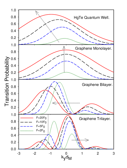
In Fig. 2 we plot the Zener transition probability as function of the wavevector of the incident particle for a HgTe quantum well and for monolayer, bilayer and trilayer graphene. We plot the transition probability for several values of the electric field, =2, 5, 10 and 20, with . Here and are the electric field and length characteristic scales set by the gap of the insulator: for HgTe quantum wells and = for multilayer graphene.
The symmetry of the Hamiltonian dictates that =. Except for monolayer graphene, the transition probability has a maximum at a finite value of that depends on the sign of . As a result, carriers with positive spin/isospin are mainly deflected towards one -direction when tunneling, whereas those with negative spin/isospin are deflected in the opposite direction. The overall transition probability increases with the applied electric field, see Fig. 2. At small fields the spatial extension of the forbidden region becomes very large and the Zener tunneling amplitude goes to zero abruptly when . This is the origin of the switching behavior of the Zener diodes. For moderate applied electric fields the asymmetry in the angle of incidence also increases with the field.
IV Sudden and Adiabatic approximations
In order to shed some light on our numerical results, we have solved Eq. (3) analytically in the limit of small parallel momentum and large electric field. The analytical calculations expand the solution of the Hamiltonian in a diabatic or in an adiabatic basis, see Fig. 1(b). The first case is suitable for an unperturbed Hamiltonian that can be diagonalized in a diabatic basis, where the carriers evolve with probability one from the valence to the conduction band. We then calculate the first correction to perfect transmission in the sudden approximation, treating the rest of the Hamiltonian in first order perturbation theory. When the Hamiltonian is such that the tunneling transmission form valence to conduction band is very small, it is more convenient to use the adiabatic basis as the unperturbed one. In the adiabatic basis the carriers are completely reflected at the barrier, and the tunneling probability can be obtained as first order perturbation to the adiabatic Hamiltonian.
The Hamiltonians of the systems we are studying can be written in the form
| (4) |
This equation defines a wavevector-dependent unitary pseudospin vector . From the form of this Hamiltonian, the expectation value of the vector of matrices is either parallel, in the conduction band, or antiparallel, in the valence band, to the pseudospin. In the absence of gap, , carriers approaching perpendicularly to the barrier, , should conserve the pseudospin. In agreement with the Klein paradox, that implies perfect transmission for gapless monolayer and trilayer graphene and perfect reflection for gapless bilayer grapheneKatsnelson et al. (2006). This conservation of the pseudospin at for massless Hamiltonians would help us to choose a diabatic or adiabatic basis as the starting point in perturbation theory.
IV.1 HgTe quantum wells, diabatic basis and sudden approximation
In HgTe quantum wells, the pseudospin has the form
| (5) |
For and , the pseudospin takes the form: , and the eigenfunctions of the Hamiltonian of Eq. (1) are chiral. In this limit, the Klein paradox dictatesKatsnelson et al. (2006) that the tunneling amplitude at is unity. For finite values of and , the Klein paradox does not apply exactly, but the transmission probability at large electric fields and small values of and is close to unity. Therefore, it is convenient to work in the diabatic basis.
In the natural units of the problem, , , and , the Hamiltonian is written as:
| (10) |
The eigenvectors of define the diabatic basis, with eigenvalues , see Fig. 1(b). We represent the corresponding wavefunction in the diabatic basis as
| (11) |
where and . We define the transmission and reflection amplitude as follows: assuming that = 0 and = 1, then and . Plugging the wavefunction, Eq. (11), into the Hamiltonian of Eq. (10), we get
| (12) |
| (13) |
The amplitudes and are obtained from the asymptotic solution of Eq. (12) with the appropriate boundary conditions. For large values of it is possible to get an analytical expression for the transition. To lowest order in , the asymptotic form of is obtained by substituting in Eq. (12),
| (14) |
For small values of this integral can be evaluated using the steepest descent method. From it we obtain the interband transition probability
| (15) |
Recovering previous units, the maximum of the transition probability to lowest order in occurs at a wavevector
| (16) |
being the maximum transition probability
| (17) |
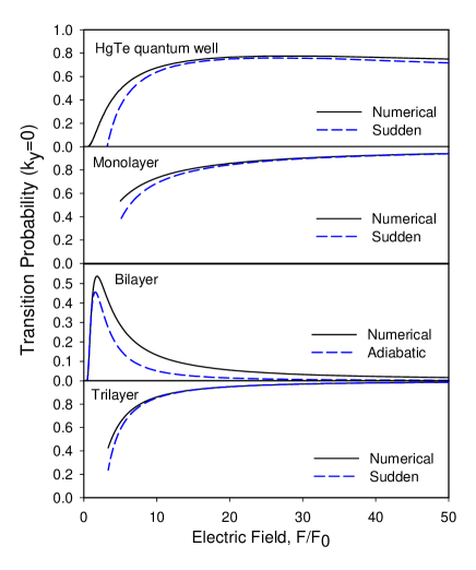
In Fig. 3 we compare the transmission at =0 obtained numerically from Eq. (3) with the one obtained from Eq. (15). The quality of the approximation is good, specially for strong electric fields. Equations (16) and (17) explain qualitatively much of the results presented in the first panel of Fig. 2: i) for each spin orientation the transition probability is asymmetric with respect to , ii) the asymmetry increases with the field, iii) the sign of depends on the product (note that when there is no spin Hall effect), iv) the asymmetry is present either for or , i.e., irrespective of whether the quantum well is in the trivial or in the topological phase, and v) the overall transition increases with the electric field. Moreover, Eqs. (16)-(17) describe quantitatively the results in the case of large . For example, for =10 we get =0.69 and , results that are in rather good agreement with the numerical ones presented in Fig. 2.
A spin dependent transmission has been also predicted to occur at the interface between a HgTe quantum well and a metalGuigou et al. (2011). In this case the asymmetry is related to localized states at the interface.
IV.2 Monolayer graphene, diabatic basis and sudden approximation
The pseudospin vector for graphene has the form
| (18) |
and for gapless monolayer graphene the Klein paradox applies exactly. Therefore, in order to study the tunneling when , it is convenient to work in the diabatic basis and, using natural units as before, we write the Bloch-like equation as
| (19) |
Note that in the reduced units, plays the same role as . The eigenvalues of the first term of Eq. (19) define the diabatic basis. Using this basis, the wavefunction takes the form
| (20) |
and the coefficients and satisfy
| (21) |
The reflection amplitude in the sudden approximation, valid in the limit, is then
| (22) |
being the transition probability, in the original units,
| (23) |
In agreement with the numerical results, we get that the transition probability is symmetric in and independent on the isospin (see Fig. 2). Note that, for monolayer graphene, the transition probability can be obtained exactlyKane and Blount (1969); Zhang and Fogler (2008),
| (24) |
and Eq. (23) corresponds to the first term in the expansion. Fig. 3, second panel, illustrates the quality of the sudden approximation at large values of the electric field.
IV.3 Bilayer graphene and the adiabatic approximation
For bilayer graphene, the pseudospin has the form
| (25) |
Gapless bilayer graphene, , is also chiral, and the pseudospin is . Holes impinging perpendicularly to the barrier from the left have opposite pseudospin than electrons moving to the right, and the same pseudospin than holes reflecting from the barrier. Therefore, the tunneling probability for and is null. When , the transition probability at is still small, see Fig. 2, and it is thus more appropriate to work in the adiabatic basis.
The Bloch equation for bilayer graphene has the form
| (26) |
where now .
The Hamiltonian in Eq. (26) defines the adiabatic basis with eigenvalues and eigenfunctions
| (27) |
where and . In order to solve Eq. (26) we consider the general solution
| (28) |
with . The coefficients and satisfy
| (29) |
with
| (30) |
Now we take the adiabatic limit, i.e., we consider that the probability to undergo a transition from one adiabatic state to another is negligible, . Then the transmission amplitude is
| (31) |
In the limit this integral can be evaluated following the methods presented in Refs. [Davis and Pechukas, 1976; Shimshoni and Gefel, 1991] and we obtain (back in physical units), see appendix A,
| (32) | |||||
where and are numerical factors. Some comments on Eq. (32) are in order: i) as shown in Fig. 3, there is a reasonable agreement between the numerical results and the one obtained in the adiabatic approximation, ii) the transition probability is not symmetric with respect to , but it is so with respect to the product , iii) the maximum transition occurs at finite , iv) there is an oscillatory term in the transmission amplitude that produces zeros in the tunneling probability at finite values of , and . These zeros appear because the bilayer graphene Hamiltonian is quadratic in the momentum and, for each energy in the gap region, there are two decaying states that interfere under the tunneling barrierNandkishore and Levitov (2011).
IV.4 Trilayer graphene, diabatic basis and sudden approximation
In ABC-stacked trilayer graphene the pseudospin unitary vector is
| (33) |
For massless trilayer graphene the pseudospin reduces to and the eigenvectors are again chiral. Because the pseudospin rotates 6 when the wavevector rotates 2 around , the transition probability at =0 is unity for massless trilayer graphene. In Fig. 2 we see that, even for , in the limit of large electric field the transition probability at small is near one. Therefore, it is appropriate to work in the diabatic basis and use the sudden approximation. We write the Bloch equation as the sum of a diabatic term plus a perturbation,
| (34) |
and in the case of the trilayer graphene we have
| (35) |
The eigenfunctions of the first term of Eq. (34) define the diabatic basis. In this basis the wavefunction takes the form
| (36) |
and the coefficients and satisfy
| (37) |
To lowest order in and , the reflection amplitude is
| (38) | |||||
and the transmission probability, in the physical units, is
| (39) |
V Berry phase and lack of reflection symmetry
The question that remains is the physical origin of the asymmetry, for a fixed spin/valley, of the tunneling amplitude as a function of . The asymmetry is not related to Chern number associated with the chirality of the massless, , HamiltoniansPrada et al. (2011). Although HgTe and monolayer graphene share the same Chern number, in monolayer graphene the transition amplitude is symmetric with respect , whereas it is not so in HgTe quantum wells.
We associate the asymmetry with the winding of the expectation value of the pseudospin when a carrier is adiabatically reflected by the tunneling barrier. This is related to the sign of the Berry phase acquired by the carrier’s pseudospin in this process.
Consider a quasiparticle moving in the valence band in the presence of a constant electric field, . This quasihole coming from and moving towards the right has a momentum . Upon arriving into the gapped region, it is adiabatically reflected from it back to with momentum . In the presence of the electric field, the momentum is not a good quantum number and it is not conserved. In a semiclassical/adiabatic approximation the momentum is defined by the relation
| (40) |
In the reflection process the pseudospin describes a trajectory on the Bloch sphere of radius unity. When the trajectory closes a circuit in the unit sphere, the wavefunction of the carrier acquires a Berry phase equal to half the solid angle defined by the surface enclosed by the circuit .
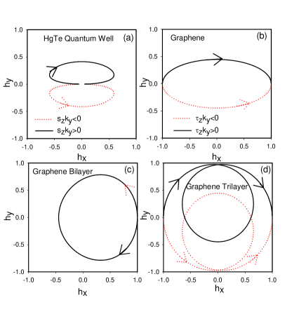
In Fig. 4 we plot, for the different Hamiltonians studied in this paper, the in-plane projection of the trajectories defined by the pseudospin when the carrier goes from to the barrier and is reflected adiabatically back to . In the case of monolayer graphene such trajectory defines an open line, both for greater or smaller than zero. Thus, for monolayer graphene there are no closed paths in the adiabatic process and there is no Berry phase associated with the reflection. The situation is different for HgTe quantum wells. In this case the trajectory defines a closed circuit and there is a Berry phase associated with the adiabatic reflection. The sign of the Berry phase depends on the direction in which the closed loop is traversed by the pseudospin. It turns out that it has opposite sign for opposite signs of or . Therefore, the sign of the Berry phase depends on the sign of the product . For graphene multilayers, , the pseudospin trajectory in the adiabatic reflection process always defines closed paths that have opposite orientation for opposite values of the product . The dependence of the Berry phase on the product , being the spin or the valley index, breaks the reflection symmetry in each index and explains the asymmetry of the transmission for a momentum at a fixed index .
VI Zener tunneling current
Finally, we calculate the tunneling current flowing through the Zener diode. We consider a - junction as the one sketched in the inset of Fig. 5. represents the built-in potential induced by doping or electrical gates, and is the source-drain potential difference. is the junction length. Within the Landauer approximation, the tunneling current for index moving in the positive -direction has the form
| (41) | |||||
where is the Fermi-Dirac distribution and is the transverse length of the - interface. Although in the uniform field approximation the transition amplitude is energy independent, the limits of the integral in depend on energy through the relation . The current flowing in the negative -direction, , is obtained performing the integral in from to . As the transition is dominated by small values of , see Fig. 2 and Ref. Nandkishore and Levitov, 2011, we approximate by in the calculation of the currents. For zero temperature the current gets the form
| (42) |
This current verifies the symmetries = and =.
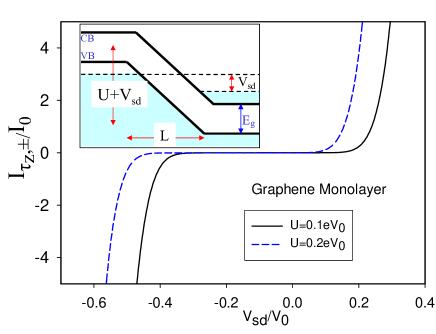
In Fig. 5 we plot the - characteristics for monolayer graphene and different values of . The curves present the breakdown-type behavior characteristic of a Zener diode. In the case of monolayer graphene the transmission amplitude is symmetric with respect to the momentum and the current is equal for positive and negative -direction.
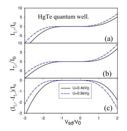
In Fig. 6 we plot the - curves for a HgTe quantum well and different values of . For spin up there is an excess of current in the negative -direction. This effect is the opposite for spin down electrons. These results indicate the existence of a spin current perpendicular to the Zener barrier. This Zener tunneling spin Hall effect is a consequence of the asymmetry in the transition curves of Fig. 2. From Fig. 6 we obtain that the Hall spin current can be as large as 30 per cent of the electrical current. Because a HgTe quantum well may be a two-dimensional topological insulator under certain conditions, there is an extra contribution to the current in this case coming from the spin-polarized edge states developed in the barrier region. However, its magnitude is always of the order of one conductance quantum or less, since the electric field diminishes itDóra and Moessner (2011). On the other hand, the Zener tunneling spin Hall current is proportional to the transverse length , see Eq. (42), and increases with the electric field.
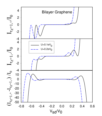
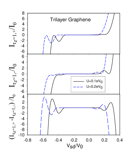
In Figs. 7 and 8 we plot the - characteristic curves for bilayer and trilayer based Zener diodes. In both cases there are some oscillations on top of the non-lineal, N-shaped - curves. These negative differential conductivities appear for positive and negative -directions, and they have their origin in the interference between decaying states in the energy gap regionNandkishore and Levitov (2011). In trilayer graphene the negative differential conductivity is even stronger than in bilayer graphene. At large source-to-drain voltage, the asymmetry of the tunneling amplitude is reflected in an excess of current in the negative -direction with respect to the positive -direction. For multilayer graphene, this effect is the opposite depending on the valley . These results indicate the existence of a valley current perpendicular to the Zener barrier that is a consequence of the asymmetry in the transition curves of Fig. 2.
VII Summary
We have analyzed Zener diode physics in HgTe quantum wells and multilayer graphene. In the case of HgTe quantum wells we find that, after traversing the barrier, a Zener tunneling spin Hall current is developed to the right of the diode. In the case of bilayer and trilayer graphene the Zener diode generates a valley Hall current. This effect is absent for the monolayer graphene. The magnitude and polarization of the Hall currents increase with the applied electric field.
The tunneling current is obtained from the transmission probability that is computed numerically in the constant electric field approximation. The origin of the Hall currents is the asymmetry of the transmission probability in the momentum perpendicular to the tunneling barrier. We have developed an analytical approximation for the tunneling transmission at small that agrees rather well with the numerical results. The physical origin of the Zener tunneling asymmetry on is related to the Berry phase that the carriers acquire when they are adiabatically reflected from the tunneling region.
In the case of multilayer graphene the Zener tunneling valley Hall effect could be used for valleytronic applicationsRycerz et al. (2007); Xiao et al. (2007). In an appropriated geometry, the asymmetry in the Zener tunneling should enable to spatially separate the carriers of each valleySchomerus (2010), which could be useful to manipulate the valley degree of freedom in bulk garphene.
The Zener tunneling spin Hall effect we predict to occur in HgTe quantum wells could be used for electrical manipulation of the spin currents. The spin currents in the Zener device should be stronger than those occurring in diffusive systems, and they could be detected in non local electrical measurements in H-shaped structuresC. Brune et al. (2010).
Acknowledgements.
We acknowledge fruitful discussions with B. Dóra, S. Kohler and M. O. Goerbig. Funding for this work was provided by MICINN-Spain via grant FIS2009-08744, the CSIC JAE-Doc program, and was supported in part by the National Science Foundation under Grant No. NSF PHY05-51164.Appendix A
In this appendix we evaluate the integral of Eq. (31). In the limit , the transition probability takes the form
| (43) |
In terms of , the integral has simple poles in the complex plane at , where . Expanding the value of near we find
| (44) |
and we rewrite
| (45) |
We solve this integral by closing the path around the lower half of the complex plane. This path encloses the poles and their associated branches. The integral then yields
| (46) |
with and .
References
- Sze (1981) S. M. Sze, Physics of Semiconductor Devices (Wiley, 1981).
- Zener (1934) C. Zener, Proc. Royal Soc. London p. 523 (1934).
- Wittig (2005) C. Wittig, J. Phys. Chem. B 109, 8428 (2005).
- Kane and Blount (1969) E. O. Kane and E. Blount, Tunneling Phenomena in Solids (Plenum Press,, New York, 1969).
- Shevchenko et al. (2010) S. N. Shevchenko, S. Adshab, and F. Nori, Physics Reports 492, 1 (2010).
- Shimshoni and Gefel (1991) E. Shimshoni and Y. Gefel, Annals Phys. 201, 16 (1991).
- X.-L. Qi et al. (2006) X.-L. Qi et al., Phys. Rev. B 74, 085308 (2006).
- B. Bernevig et al. (2006) B. Bernevig et al., Science 314, 1757 (2006).
- M. König et al. (2007) M. König et al., Science 318, 766 (2007).
- L. Fu et al. (2007) L. Fu et al., Phys. Rev. Lett. 98, 106803 (2007).
- J. E. Moore etal. (2007) J. E. Moore etal., Phys. Rev. B 75, 121306 (2007).
- Murakami (2007) S. Murakami, New Journal of Physics 9, 356 (2007).
- Novoselov et al. (2004) K. S. Novoselov, A. K. Geim, S. V. Mozorov, D. Jiang, Y. Zhang, S. V. Dubonos, I. V. Gregorieva, and A. A. Firsov, Science 306, 666 (2004).
- Novoselov et al. (2005) K. S. Novoselov, D. Jiang, T. Booth, V. V. Khotkevich, S. M. Morozov, and A. K. Geim, Nature 438, 197 (2005).
- Zhang et al. (2005) Y. Zhang, Y.-W. Tan, H. L. Stormer, and P. Kim, Nature 438, 201 (2005).
- Katsnelson et al. (2006) M. I. Katsnelson, K. S. Novoselov, and A. Geim, Nat. Phys. 2, 620 (2006).
- Cheianov and Fal’ko (2006) V. V. Cheianov and V. I. Fal’ko, Phys. Rev. B 74, 041403 (2006).
- Williams et al. (2007) J. R. Williams, L. DiCarlo, and C. M. Marcus, Science 317, 638 (2007).
- Zhang and Fogler (2008) L. M. Zhang and M. M. Fogler, Phys. Rev. Lett. 100, 116804 (2008).
- Young and Kim (2009) A. Young and P. Kim, Nat. Phys. 5, 222 (2009).
- Vandecasteele et al. (2010) N. Vandecasteele, A. Barreiro, M. Lazzeri, A. Bachtold, and F. Mauri, Phys. Rev. B 82, 045416 (2010).
- Stander et al. (2009) N. Stander, B. Huard, and D. Goldhaber-Gordon, Phys. Rev. Lett. 102, 026807 (2009).
- Jena et al. (2008) D. Jena, T. Fang, Q. Zhang, and H. Xing, Applied Physics Letters 93, 112106 (2008).
- Chiu et al. (2010) H.-Y. Chiu, V. Perebeinos, Y.-M. Lin, and P. Avouris, Nano Letters 10, 4634 (2010).
- Brey and Fertig (2009) L. Brey and H. A. Fertig, Phys. Rev. Lett. 103, 046809 (2009).
- Arovas et al. (2010) D. P. Arovas, L. Brey, H. A. Fertig, E.-A. Kim, and K. Ziegler, New Journal of Physics 12, 123020 (2010).
- Nandkishore and Levitov (2011) R. Nandkishore and L. Levitov, Proceedings of the National Academy of Sciences 108, 14021 (2011).
- (28) Typical parameters for HgTe quantum wells areG. Tkachov et al. (2011), , , .
- Kane and Mele (2005a) C. L. Kane and E. J. Mele, Phys. Rev. Lett. 95, 226801 (2005a).
- Kane and Mele (2005b) C. L. Kane and E. J. Mele, Phys. Rev. Lett. 95, 146802 (2005b).
- Prada et al. (2011) E. Prada, P. San-Jose, L. Brey, and H. Fertig, Solid State Communications 151, 1075 (2011).
- Castro-Neto et al. (2009) A. H. Castro-Neto, F.Guinea, N.M.R.Peres, K.S.Novoselov, and A.K.Geim, Rev. Mod. Phys. 81, 109 (2009).
- Min et al. (2008) H. Min, G. Borghi, M. Polini, and A. H. MacDonald, Phys. Rev. B 77, 041407 (2008).
- McCann et al. (2007) E. McCann, D. S. Abergel, and V. I. Fal’ko, Solid State Communications 143, 110 (2007).
- Hasan and Kane (2010) M. Z. Hasan and C. L. Kane, Rev. Mod. Phys. 82, 3045 (2010).
- Qi and Zhang (2011) X.-L. Qi and S.-C. Zhang, Rev. Mod. Phys. 83, 1057 (2011).
- Guigou et al. (2011) M. Guigou, P. Recher, J. Cayssol, and B. Trauzettel, Phys. Rev. B 84, 094534 (2011).
- Davis and Pechukas (1976) J. Davis and P. Pechukas, J.Chem.Phys. 64, 3129 (1976).
- Dóra and Moessner (2011) B. Dóra and R. Moessner, Phys. Rev. B 83, 073403 (2011).
- Rycerz et al. (2007) A. Rycerz, J. Tworzydlo, and C. W. J. Beenakker, Nature Physics 3, 172 (2007).
- Xiao et al. (2007) D. Xiao, W. Yao, and Q. Niu, Phys. Rev. Lett. 99, 236809 (2007).
- Schomerus (2010) H. Schomerus, Phys. Rev. B 82, 165409 (2010).
- C. Brune et al. (2010) C. Brune et al., Nat.Phys. 6, 448 (2010).
- G. Tkachov et al. (2011) G. Tkachov et al., Phys. Rev. Lett. 106, 076802 (2011).