New interpretation of the origin of 2DEG states at the surface of layered topological insulators
Abstract
On the basis of relativistic ab-initio calculations we show that the driving mechanism of simultaneous emergence of parabolic and M-shaped 2D electron gas (2DEG) bands at the surface of layered topological insulators as well as Rashba-splitting of the former states is an expansion of van der Waals (vdW) spacings caused by intercalation of metal atoms or residual gases. The expansion of vdW spacings and emergence of the 2DEG states localized in the (sub)surface region are also accompanied by a relocation of the topological surface state to the lower quintuple layers, that can explain the absence of interband scattering found experimentally.
pacs:
73.20.-r, 79.60.-iThe recently discovered three-dimensional topological insulators belong to a class of insulators in which the bulk gap is inverted due to the strong spin-orbit interaction Fu_PRL_07 ; Fu_PRB_07 ; Qi_PRB_08 ; Zhang_NatPhys_09 . A direct consequence of such bulk band structure arises at the surface: the spin-polarized topologically protected massless metallic states, forming a Dirac cone. These surface states (SS) exhibit many interesting properties resulting from the fact that the spin of electron is locked perpendicular to its momentum, thus forming a SS spin structure that protects electrons from backscattering under the influence of weak perturbations. This makes topological insulators potentially promising materials for creation of new quantum devices.
By now few families of topological insulators (TI) have been discovered Shitade ; Chadov ; Lin_MN2010 ; EremeevJETPLettTh ; Lin_PRL2010 ; Kuroda_PRL2010 ; EremeevJETPL_PBT ; Xia_NatPhys2009 ; ChenScience09 ; ZhangPRL09 ; KurodaPRL10 , of which the binary layered compounds Bi2Te3, Bi2Se3, and Sb2Te3 are the most studied both experimentally Xia_NatPhys2009 ; ChenScience09 ; ZhangPRL09 ; KurodaPRL10 and theoretically Zhang_NatPhys_09 ; EremeevJETPL_10 ; ZhangNatPhys10 ; SongPRL10 ; ZhangNJP10 ; Yazyev_PRL2010 . The latter systems have tetradymite-like layered structure with ionic-covalent bonded quintuple layer (QL) slabs, which are linked by weak van der Waals forces. Such a layered structure predetermines the formation of the surface by cleavage on the van der Waals (vdW) spacing that doesn’t result in the formation of dangling bonds, and thus only the Dirac states reside in the bulk energy gap.
However, recently in several studies it has been demonstrated by using angle-resolved photoemission spectroscopy (ARPES) that beside the Dirac cone the 2DEG states arise at the surface of Bi2Se3 after a few hours of exposition in vacuum Bianchi , upon deposition of various magnetic Wray_NatPhys11 ; Valla and non-magnetic atoms Valla ; Wray_arXiv ; Zhu_arXiv , and molecules as well Benia_arXive ; Wray_arXiv . These states form a parabolic band (PB) in the energy gap just below the conduction band and M-shaped band in the local gap of bulk-projected valence band. The former bands show an appreciable Rashba spin splitting King_Arxiv ; Wray_NatPhys11 ; Valla ; Benia_arXive ; Zhu_arXiv . Moreover, for several adsorbates Valla ; Zhu_arXiv at the saturation deposition time a second and even third pair of spin-split parabolic states emerges below the conduction band minimum. In the most of these papers the emergence of PB states was ascribed to a confinement of the conduction band states in a quantum well formed by band bending potential produced by adsorption of metallic atoms or residual gases, although in Ref. Benia_arXive it was pointed out that the potential gradient from band bending cannot alone be responsible for their Rashba-splitting. Indeed, a model calculation exploiting band bending approach based on the coupled solution of the Poisson and Schrödinger equations yielded the Rashba spin-orbit coupling parameter which is significantly smaller than that extracted from the ARPES data King_Arxiv . Moreover this approach doesn’t reproduce the M-shaped band Bianchi . The most surprising experimental finding is the absence of interband scattering of the Dirac state electrons in the presence of the PB spin-split states after the deposition of any kind of metal atoms Valla . A study of a naturally aged surface of Bi2Se3 also reveals that scattering rate in the topologically protected state is unaffected by the potential created by adsorbed atoms or molecules Park_PRB10 .
In this Letter we propose an alternative explanation of the emergence of the 2DEG states based on a well known fact: the interlayer gaps (vdW spacings) in the layered compounds can serve as natural containers for impurities in synthesis processes and for intercalated atoms. Various atoms have been intercalated in different layered materials, inducing expansion of vdW spacings Dresselhaus ; Friend ; ILM . One would expect that due to a weak binding between QLs even a relatively small concentration of contaminants in the vdW gap can produce its sizeable expansion. The magnitude of this expansion depends on the impurity size and on formation of impurity atom clusters within the vdW gap. Mechanisms of diffision of adsorbed atoms into the vdW gap are not known in detail yet, however, at least two kinds of the diffusion process can be anticipated. First, the Fermi level of naturally grown crystals of the tetradymite-like TI is usually found to be located in the bulk conduction band due to vacancy defects Xia_NatPhys2009 ; KurodaPRL10 and, thus, apparently there is a sufficiently high vacancy concentration to ensure the vacancy mediated penetration of impurities through a QL into the vdW gap. The second process can be associated with the sliding of impurity atoms into the vdW gap from step edges.
Here we show on the basis of ab-initio calculations using the VASP code VASP1 ; VASP2 that the driving mechanism of the simultaneous emergence of the parabolic and M-shaped bands in Bi2Se3, Bi2Te3, and Sb2Te3, is a widening of the outermost vdW spacing. This scenario also explains the Rashba-type splitting for the PB. We find that besides the emergence of PB states, which are localized in the detached QL the expansion of the vdW spacing results in a relocation of the Dirac state to the lower QL that makes topological and PB states separated in space. This fact explains the observable absence of interband scattering Valla ; Park_PRB10 . We also show that the expansion of various vdW gaps produces multiple 2DEG states.
| expansion | (eVÅ) | |||||
|---|---|---|---|---|---|---|
| (%) | (eV) | - | - | - | - | |
| Bi2Se3 | 10 | 0.30 | 0.38 | 0.46 | 0.16 | 0.14 |
| 20 | 0.27 | 0.27 | 0.28 | 0.25 | 0.24 | |
| 30 | 0.24 | 0.20 | 0.20 | 0.33 | 0.32 | |
| 40 | 0.22 | 0.18 | 0.18 | 0.29 | 0.29 | |
| 50 | 0.19 | 0.17 | 0.17 | 0.24 | 0.24 | |
| Bi2Te3 | 10 | 0.15 | 0.31 | 0.37 | 0.29 | 0.28 |
| 20 | 0.04 | 0.17 | 0.18 | 0.40 | 0.40 | |
| 30 | 0.01 | 0.14 | 0.13 | 0.74 | 0.71 | |
| 40 | 0.00 | 0.12 | 0.12 | 0.59 | 0.57 | |
| 50 | -0.02 | 0.12 | 0.13 | 0.45 | 0.45 | |
| Sb2Te3 | 10 | 0.09 | 0.24 | 0.28 | 0.30 | 0.30 |
| 20 | 0.08 | 0.17 | 0.18 | 0.35 | 0.36 | |
| 30 | 0.05 | 0.12 | 0.13 | 0.26 | 0.26 | |
| 40 | 0.04 | 0.12 | 0.12 | 0.15 | 0.15 | |
| 50 | 0.02 | 0.12 | 0.12 | 0.10 | 0.10 | |
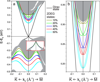
We start with consideration of the Bi2Se3 surface. To simulate the effect of the adsorbate deposition time as well as the impurity atom size we perform a calculation of the Bi2Se3 surface with expansion of the outermost vdW spacing by 10% - 50%. As one can see (Fig. 1), the detachment of the outermost QL leads to the simultaneous emergence of both the Rashba-split band below the bottom of the bulk conduction band and the M-shaped band in the valence bulk-projected gap. The energy of the M-shaped and parabolic spin-split bands as well as the magnitude of the Rashba splitting parameter strongly depend on the vdW spacing expansion. At 10% expansion the first pair of spin-split bands as well as the M-shaped state emerges just below the bulk projected states. Upon increasing the vdW expansion these bands shift gradually down. This behavior reflects the rise of the 2DEG bands as a function of the deposition time found in recent experimental studies Valla ; Benia_arXive . Up to 30% expansion this also leads to the decrease of the effective mass of PBs and to the increase of the Rashba coupling parameter (see Table 1). At the same time demonstrates an apparent -- anisotropy at 10% expansion. At higher expansions this anisotropy is significantly reduced. The small () anisotropy was also obtained in Ref. King_Arxiv (SI). Different fitting procedures for the ARPES measured band in Ref. King_Arxiv (SI) gave the Rashba splitting parameter varying from 0.36 to 1.35 eVÅ in aged Bi2Se3 surface. In the case of potassium deposition on Bi2Se3 a maximal eVÅ was observed after 2.5-3 minute K evaporation Zhu_arXiv . Our model gives a lower limit for the former case at moderate expansions and underestimates the latter maximal while the band bending model King_Arxiv gives 0.1 eVÅ for the PB splitting.
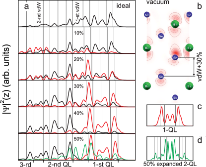
The nature of spin-split PBs can be deduced from analysis of their spacial localization. At 10% expansion the emerged parabolic state, which splits off from the conduction bulk band continuum, keeps yet a bulk-like delocalized character (Fig. 2(a)). This explains the obtained -- anisotropy of the parabolic band at small expansions: it just reflects a similar anisotropy of the bulk states. Upon increasing the vdW spacing this state acquires more localized character and at 30-50% it almost completely lies in the detached QL. The PB state, characterized by four peaks localized in the outermost QL, Fig. 2(a), reflects the symmetry of the energy gap edges at : it is composed of the Bi orbitals (lower edge of the gap) with the sizeable Se contribution (upper edge of the gap) to the vdW-side peak (Fig. 2(b)). With the further increase of the outermost vdW spacing the localization of the parabolic state approaches the distribution of the lowest unoccupied band in a free-standing QL (Fig. 2(c)). The latter band is not spin-orbit split since a free-standing QL possess inversion symmetry. This effect accounts for the reduction of in the PB states with the increase of the vdW spacing beyond 30% (Table 1). Note here that a large concentration of intercalated atoms in the vdW gap can affect the vdW-side Se orbitals and hence lead to change of some features of the spin-split band, for instance increase the Rashba splitting.
In the case of Bi2Te3 and Sb2Te3 we find the same trend in the development of the Rashba-split PB (Table 1). However, the heavier Te provides two times bigger in Bi2Te3 with respect to that in Bi2Se3 while the lighter Sb, in turn, gives a smaller Rashba coupling parameter in Sb2Te3.
An intriguing finding is that the development of PB states is accompanied by shifting the topological state deep into the crystal, so that at 30-50% expansion the Dirac state is mostly located in the second QL, beneath the detached QL. In this case wave functions of the topological and parabolic states only slightly overlap. The latter explains the experimentally observed absence of interband scattering Valla ; Park_PRB10 . It should be stressed that the dispersion of the upper part of the Dirac cone as well as the position of the Dirac point remain unchanged under this relocation while the dispersion of the lower part of the Dirac cone is slightly modified (Fig. 1(a), insert) in agreement with ARPES data Wray_arXiv .
The M-shaped band emerges in the local gap of the bulk-projected valence band splitting off from the upper edge of the gap. The edge is formed by the bulk Se states only which are not spin-orbit split at and around. The M-shaped SS being split off from the Se bands does not acquire other symmetry and thus does not show spin-orbit splitting at small momenta. Only being close to the bulk continuum states (at large momenta) it shows weak spin-orbit splitting. With the increase of the vdW gap it becomes more localized. Charge density of this state as shown for 50% expansion case in Fig. 2(a) is mostly situated in the expanded vdW gap and around. Comparing this with that of the the upper occupied state in free-standing 2-QL with 50% vdW gap expanded, Fig. 2(d), one can note that these two states are of the same origin: the vdW spacing expansion.
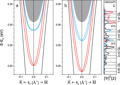
Now we consider the effect of simultaneous expansion of the first and second vdW spacings. The expansion of the latter can be caused by further diffusion in the sample of a smaller amount of atoms deposited on the surface. In Fig. 3(a) we show the band spectrum of Bi2Se3 with 40% and 10% expanded 1-st and 2-nd vdW spacings, respectively. This film geometry gives rise to the second parabolic state below the conduction band. This state shows very small spin splitting. The emergence of the second PB leads to a decrease of energy of the first band by 20 meV as well as a reduction of its to 0.27 eVÅ compared to the case of the single vdW spacing expansion by 40%. Further increase of the 2-nd vdW gap leads to a subsequent downshift of both PBs (Fig. 3(b)). While for the upper band in this case is 0.16 (0.15) eVÅ in - (-) directions, respectively, the spin splitting of the lower state is reduced to 0.25 eVÅ. Localizations of the lower and upper bands in general resemble those for a single vdW expansion by 40% and 20%, respectively except their mutual overlap (Fig. 3(c)). The overlap of the topological SS with that localized in the 2-nd QL is similar to that in the single 20% case while the Dirac state is absent in the outermost QL as in the case of the single 40% detachment. Further increase of the 2-nd vdW spacing leads to bigger downshift of both PBs, to increase of their overlap and complete relocation of the Dirac state to the third QL. The expansion of the second vdW spacing also results in the development of the second M-shaped state in the valence band gap (not shown). Subsequently expansion of the third vdW gap, that simulate a deeper diffusion of deposited atoms, leads to simultaneous emergence of the third pair of parabolic Rashba-split and M-shaped bands (not shown).
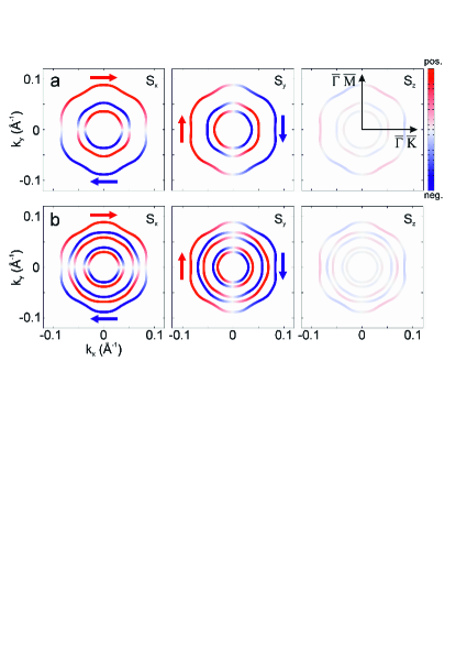
Note that the sizeable overlap between the topological SS and 2DEG state exists barely at the beginning of the formation of each new PB and hence the interband scattering is possible in a narrow energy interval just below the conduction band only. In fact this scattering will be also limited by spin conservation rule due to spin polarized nature of both topological and 2DEG Rashba-split states. The Dirac state has clockwise spin helicity while the parabolic states demonstrate typical Rashba-type counter-clockwise and clockwise helicities for outer and inner branches, respectively, with a very small spin component for both types of SS’s (Fig. 4(a)). This spin structure allows “ to ” scattering between the topological state and the inner branch of the PB and “ to ” transitions between the Dirac cone state and the outer branch of the PB. However, the efficiency of these transitions should be significantly reduced because of small overlap between the topological SS and PB state for well developed PBs. In the case of multiple detached vdW gaps new channels for scattering of Dirac electrons (Fig. 4(b)) arise, nevertheless, only PBs that have sizeable overlap with the topological SS can contribute to considerable interband scattering.
To summarize, on the base of the proposed scenario of impurity intercalation in the vdW gaps of the layered TIs and ab-initio calculation results we have shown that the driving mechanism of experimentally observed simultaneous emergence of parabolic and M-shaped bands as well as Rashba-splitting of former bands is expansion of vdW spacings. These bands are 2DEG states localized in the narrow (sub)surface region. We have found that besides the development of 2DEG SS’s the expansion of the vdW gap also provides relocation of the topological state to the lower QL. This fact explains the observed absence of interband scattering between the topological SS and Rashba-split PB states. We also show that expansion of the low-lying vdW gaps produces multiple 2DEG states. The proposed mechanism is expected to be also valid for other layered TIs.
We acknowledge partial support by the University of the Basque Country (project GV-UPV/EHU, grant IT-366-07) and Ministerio de Ciencia e Inovación (grant FIS2010-19609-C02-00). We thank Ph. Hofmann, A. Kimura, Yu.M. Koroteev, and E.E. Krasovskii for enjoyable discussions.
References
- (1) L. Fu, et al., Phys. Rev. Lett. 98, 106803 (2007).
- (2) L. Fu, and C.L. Kane, Phys. Rev. B 76, 045302 (2007).
- (3) X.L. Qi, et al., Phys. Rev. B 78, 195424 (2008).
- (4) H. Zhang, et al., Nature Phys. 5, 438 (2009).
- (5) A. Shitade et al., Phys. Rev. Lett. 102, 256403 (2009).
- (6) S. Chadov et al., Nature Mater. 9, 541 (2010).
- (7) H. Lin et al., Nature Mater. 9, 546 (2010).
- (8) S. V. Eremeev, et al., Pis’ma Zh. Eksp. Teor. Fiz. 91, 664 (2010) [JETP. Lett. 91, 594 (2010)].
- (9) H. Lin, et al., Phys. Rev. Lett. 105, 036404 (2010).
- (10) K. Kuroda, et al., Phys. Rev. Lett. 105, 146801 (2010).
- (11) S. V. Eremeev, et al., Pis’ma Zh. Eksp. Teor. Fiz. 92, 183 (2010) [JETP. Lett. 92, 161 (2010)].
- (12) Y. Xia, et al., Nature Phys. 5, 398 (2009).
- (13) Y. L. Chen, et al., Science, 325, 178 (2009).
- (14) T. Zhang, et al., Phys. Rev. Lett. 103, 266803 (2009).
- (15) K. Kuroda et al., Phys. Rev. Lett. 105, 076802 (2010).
- (16) Y. Zhang, et al., Nature Phys. 6, 584 (2010).
- (17) J. H. Song, et al., Phys. Rev. Lett. 105, 096403 (2010).
- (18) W. Zhang, et al., New J. Phys. 12, 065013 (2010).
- (19) S.V. Eremeev, et al., Pis’ma Zh. Eksp. Teor. Fiz. 91, 419 (2010) [JETP. Lett. 91, 387 (2010)].
- (20) O.V. Yazyev, et al., Phys. Rev. Lett. 105, 266806 (2010).
- (21) M. Bianchi, et al., Nature Comm. 1:128 DOI: 10.138/ncomms1131 (2010).
- (22) P.D.C. King, et al., arXiv:1103.3220.
- (23) L.A. Wray, et al., Nature Phys. 7, 32 (2011).
- (24) Z.-H. Pan, et al., arXiv:1104.0966v1
- (25) L.A. Wray, et al., arXiv:1105.4794v1
- (26) Z.-H. Zhu, et al., arXiv:1106.0552v1
- (27) H.M. Benia, et al., arXiv:1105.2664v1.
- (28) S.R. Park, et al., Phys. Rev. B 81, 041405(R) (2010).
- (29) M.S. Dresselhaus and G. Dresselhaus, Adv. Phys. 51, 1 (2002).
- (30) R.H. Friend and A.D. Yoffe, Adv. Phys. 36, 1 (1987).
- (31) Intercalation in Layered Materials, edited by M.S. Dresselhaus (Plenum, New York, 1986).
- (32) G. Kresse, J. Furthmüller, Phys. Rev. B 54, 11169 (1996).
- (33) G. Kresse, D. Joubert, Phys. Rev. B 59, 1758 (1998).