Generation of high-order optical vortices using directly machined spiral phase mirrors
Abstract
We report on the generation of high-order optical vortices by spiral phase mirrors. The phase mirrors are produced by direct machining with a diamond tool and are shown to produce high-quality optical vortices with topological charges ranging from 1 to 1000 at a wavelength of 532 nm. The direct machining technique is flexible and offers the promise of high-precision, large-diameter spiral phase mirrors that are compatible with high optical powers.
I Introduction
Optical vortices are light beams that carry orbital angular momentum and are characterised by a phase that increases azimuthally about a singularity at the centre of the beamCoullet:1989p2463 . These beams can be generated directly in a cylindrically symmetric laser cavity. It is, however, simpler in practice to approximate them by illuminating diffractive optics with more readily available laser modesHeckenberg:1992p4137 ; Beijersbergen:1994p2791 ; Kennedy:2002p3945 .
A variety of possible applications for optical vorticesFrankeArnold:2008p3716 have driven research into their production. These applications include optical trapping and manipulation of colloidal particlesGrier:2003p844 and cold atomsKuga:1997p5064 , the generation of Bose-Einstein condensate vorticesNatarajan:2006p4907 , phase-contrast microscopyBernet:2006p3400 , image filtering for extra-solar planet detectionLee:2006p3375 , stimulated emission depletion (STED) microscopyWillig:2006p3766 and the encoding of optical quantum informationMair:2001p2490 .
The considerable utility of optical vortices has driven the development of several methods for their production. Most commonly, a phase shift of the form is applied to an incident laser beam where is the topological charge and is the azimuthal coordinate about the beam centre in the transverse plane.
One method to apply the required phase shift is to use a computer-controlled spatial-light modulator (SLM)Sundbeck:2005p2535 . This approach has the considerable advantages of being flexible and allowing the phase profile to be dynamically varied on 10 ms timescales. SLM’s, however, suffer from high cost and limited spatial and phase resolution. Conversion efficiencies can be quite high for low-order optical vortices but begin to suffer from resolution limits as the order is increased.
Another approach is to use lithographic processes to construct a phase maskKennedy:2002p3945 ; Moh:2006p2223 ; Kotlyar:2008p4053 . These phase masks have restrictions in terms of phase resolution, spatial resolution, maximum phase shift and useable area, although advanced lithographic techniques can relax many of these restrictions.
Here, we report on the production by direct machining of spiral phase mirrors (SPMs) that are suitable for generating optical vortices. We demonstrate that the resultant phase mirrors can deterministically produce high-quality optical vortices over a large range of topological charges from 1 to 1000. These mirrors can be produced economically and the size of the optics is restricted only by the geometry of the machining enclosure.
II Fabrication
The SPMs are machined from aluminium using a single-crystal diamond tool. The machining is performed by an ultra-precision lathe, produced by Moore Nanotechnology. The tool position relative to the part surface is adjusted while the part is rotated at a constant rate on the spindle. High-resolution position encoders ensure that the tool is positioned with nanometric precision for each point on the part surface.

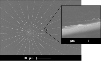
The cutting speed is limited by the acceleration of the lathe’s linear axes, although we can relax this restriction by breaking the SPM into segments. Each segment is a linear ramp with a total height corresponding to a phase shift. Figure 1 shows an SEM image of a charge 100 SPM composed of 25 segments, each of which imparts an phase ramp. For the charge 100 SPM, we estimate that the central defect accounts for 0.006% of the total mirror surface, while the sharp jumps between segments collectively account for approximately 3% of the total area.
For our analysis, we produced 25 mm diameter optics, which required cutting times ranging from 30 minutes to two hours for charges of 1 to 100, respectively. The size of the optic can be scaled without losing quality or increasing cutting time simply by selecting a diamond tool of an appropriate radius.
III Results
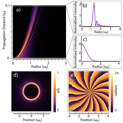
To verify the performance of our phase plate, we made transverse beam profile measurements that can be compared to theoretical models. The illumination of an SPM with a TEM00 mode results in a beam profile that can be expressed as a hypergeometric Gaussian mode (HyGG)Karimi:2007p3929 . These modes have a cylindrically symmetric amplitude and propagate from a Gaussian profile at the SPM into a ring-shaped profile in the far-field. Figure 2 a) shows the calculated radial amplitude of a propagating charge 15 HyGG mode immediately after it is created.
Experimental intensity profiles are obtained by illuminating machined SPMs with a 532 nm laser beam that has been transmitted through a mode-cleaning cavity locked to the TEM00 mode. The resulting intensity patterns are recorded on a CCD camera. The radial intensity distribution is then obtained by fitting an interpolating function to the raw pixel data and integrating the resultant function azimuthally in polar co-ordinates. The experimental data is normalised such that the area under the curve is equal to that of the normalised HyGG integrated over the same region.

Figures 2 b) and c) show the calculated (dashed blue) and measured (solid red) radial intensity profiles after propagation through 0.096 Rayleigh lengths and at the location of the SPM, respectively. The beam waist of the input Gaussian mode is 450 and the propagation distance has been corrected from a measured 9.5 cm to 11.5 cm, a discrepancy which we attribute to the SPM not being located exactly at the beam waist. The excellent agreement of the model with our data indicates that the SPM is performing as designed. Figure 2 d) shows the intensity of a charge 15 optical vortex that has been imaged in the far-field. The phase of the vortex in the near-field, figure 2 e), has been obtained by interfering the vortex with a collimated Gaussian beam and scanning the relative phase of the two beams. CCD images of the interference patterns are captured and the phase profile is obtained by fitting a sine function to the intensity recorded at each pixel.
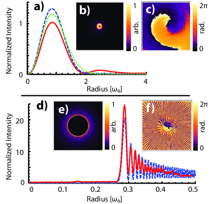
We verify that the machined SPMs produce high-quality vortices over a range of topological charges by examining the intensity and phase profiles of charge 1 and charge 100 vortices. Figure 3 (a-c) shows the results for the charge 1 vortex. Due to the slow evolution of the charge 1 vortex, imaging optics were used to record the intensity pattern and the propagation distance which was used for the calculated intensity was selected to fit the measured profile.

Figure 3 (d-f) shows the results for a charge 100 vortex. There is some deviation from the calculated intensity in the peripheral fringes; however, the primary feature is in good agreement with the calculated intensity distribution. As with the charge 15 analysis, the propagation distance was corrected to account for the SPM not being located at the beam waist. The phase profile shows three distinct regions. The central region has zero charge and originates from the undiffracted portion of the beam. An intermediate region shows a charge of 25, which we believe is an artefact of the 25 step design used to create the SPM. The inner region is, however, of little consequence because the outer region, beyond a radius of 0.25 , contains 98% of the optical power and shows the intended charge 100 optical vortex.
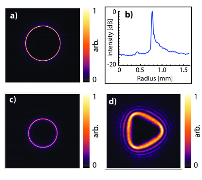
The intensity distribution of the same charge 100 vortex, imaged in a plane that features the smallest observed ring thickness, is shown in figures 4 a) and b). The minimal undiffracted order, even at high charges, is notable when compared to SLM-produced vorticesSundbeck:2005p2535 .
In an attempt to find the limits of the direct machining process, we manufactured a charge 1000 SPM; however, our ability to properly characterise the vortices degraded after a charge of roughly 100 due to limited CCD resolution. Figure 4 c) shows the measured intensity profile of the charge 1000 optical vortex.

Spiral phase mirrors that can be manufactured by this technique are not limited to linear azimuthal phase ramps. Modulated phase profilesCurtis:2003p2447 can be produced provided that the modulation is slow compared to the loop bandwidth of the positional feedback on the lathe. To demonstrate this flexibility, we cut a charge 15 optical vortex with a sinusoindally modulated phase ramp, shown in figure 4 d). The modulation has a period of and a depth of 0.1. It is also possible to cut the SPMs on a curved surface. In this way, SPMs could be created on spherical or even aspherical mirrors to provide integrated focusing optics.
IV Conclusions
We have demonstrated that the direct machining of spiral phase mirrors using a diamond tool can produce high-quality, high-charge optical vortices. In addition to low cost, technical simplicity and flexibility, this fabrication method has the advantage of being applicable to a variety of metallic and soft crystalline optical materials, which may allow the production of transmissive as well as reflective vortex producing optics.
Acknowledgments
We thank A. Luiten, A. G. White, M. Hosseini and N. Devlin for fruitful discussion. We gratefully acknowledge the technical support provided by T. Stewart and E. Alarie from Moore Nanotechnology. This research is supported by the Australian Research Council (project numbers CE110001027 and DP1092891).
References
- (1)
- (2) P. Coullet, L. Gil, and F. Rocca, Opt. Commun. 73, 403 (1989).
- (3) N. R. Heckenberg, R. McDuff, C. P. Smith, and A. G. White, Opt. Lett 17, 221 (1992).
- (4) M. Beijersbergen, R. Coerwinkel, M. Kristensen, and J. Woerdman, Opt. Commun. 112, 321 (1994).
- (5) S. A. Kennedy, M. J. Szabo, H. Teslow, J. Z. Porterfield, and E. R. I. Abraham, Phys. Rev. A 66, 043801 (2002).
- (6) S. Franke-Arnold, L. Allen, and M. Padgett, Laser & Photon. Rev. 2, 299 (2008).
- (7) D. Grier, Nature 424, 810 (2003).
- (8) T. Kuga, et. al., Phys. Rev. Lett. 78, 4713 (1997).
- (9) M. F. Andersen, et. al., Phys. Rev. Lett. 97, 170406 (2006).
- (10) S. Bernet, A. Jesacher, S. Fürhapter, C. Maurer, and M. Ritsch-Marte, Opt. Express 14, 3792 (2006).
- (11) J. H. Lee, G. Foo, E. G. Johnson, and G. A. Swartzlander, Phys. Rev. Lett. 97, 053901 (2006).
- (12) K. I. Willig, S. O. Rizzoli, V. Westphal, R. Jahn, and S. W. Hell, Nature 440, 440 (2006).
- (13) A. Mair, A. Vaziri, G. Weihs, and A. Zeilinger, Nature 412, 313 (2001).
- (14) S. Sundbeck and I. Gruzberg, Opt. Lett. 30, 477 (2005).
- (15) K. J. Moh, et. al., App. Opt. 45, 1153 (2006).
- (16) V. V. Kotlyar, A. A. Kovalev, R. V. Skidanov, S. N. Khonina, and J. Turunen, Appl. Opt. 47, 6124 (2008).
- (17) E. Karimi, G. Zito, B. Piccirillo, L. Marrucci, and E. Santamato, Opt. Lett. 32, 3053 (2007).
- (18) J. Curtis and D. Grier, Opt. Lett. 66, 872 (2003).