Thermodynamic properties of tunneling quasiparticles in graphene-based structures
Abstract
Thermodynamic properties of quasiparticles in a graphene-based structures are investigated. Two graphene superconducting layers (one superconducting component is placed on the top layered-graphene structure and the other component in the bottom) separated by oxide dielectric layers and one normal graphene layer in the middle. The quasiparticle flow emerged due to external gate voltage, we considered it as a gas of electron-hole pairs whose components belong to different layers. This is a striking result in view of the complexity of these systems: we have established that specific heat exhibits universal (-) behaviour at low , independent from the gate voltage and the superconducting gap. The experimental observation of this theoretical prediction would be an important step towards our understanding of critical massless matter.
pacs:
74.25.Jb, 81.05.ue,74.50.+r,74.45.+cI Introduction
Graphene is a unique system in many ways Novosel-1 ; Topsakal-1 ; Sahin-1 . It is truly two-dimensional systems, has unusual electronic excitations described in terms of Dirac fermions that move in a curved space, is an interesting mix of a semiconductor (zero density of states) and a metal (gaplessness), and has properties of soft matter. The electrons in graphene seem to be almost insensitive to disorder and electron-electron interactions and have very long mean free paths Denis-1 . Hence, graphene’s properties are different from what is found in usual metals and semiconductors GN-1 ; Sahin-2 . Graphene has also a robust but flexible structure with unusual phonon modes that do not exist in ordinary three-dimensional solids. In some sense, graphene brings together issues in quantum gravity and particle physics, and also from soft and hard condensed matter. Interestingly enough, these properties can be easily modified with the application of electric and magnetic fields, addition of layers, control of its geometry, and chemical doping Luis-1 ; Jun-1 . Moreover, graphene can be directly and relatively easily probed by various scanning probe techniques from mesoscopic down to atomic scales, because it is not buried inside a 3D structure Pan-1 . This makes graphene one of the most versatile systems in condensed-matter research.

Besides the unusual basic properties, graphene has the potential for a large number of applications Geim-1 , from chemical sensors Chen-1 to transistors Nel-1 ; Oos-1 . Graphene can be chemically and/or structurally modified in order to change its functionality and henceforth its potential applications. Moreover, graphene can be easily obtained from graphite, a material that is abundant on the Earth s surface. This particular characteristic makes graphene one of the most readily available materials for basic research. Whereas many papers have been written on monolayer graphene in the past few years, only a small fraction actually deal with multilayers Haas-1 ; Yan-1 . The majority of the theoretical and experimental efforts have concentrated on the single layer, perhaps because of its simplicity and the natural attraction that a one atom thick material, which can be produced by simple methods in almost any laboratory, creates. Nevertheless, few-layer graphene is equally interesting and unusual with a technological potential, perhaps larger than the single layer Bol-1 . Indeed, the theoretical understanding and experimental exploration of multilayers is far behind the single layer.
Graphene can be considered as a semiconductor with zero band gap. Electron energy spectrum of graphene contains two Dirac points that separate the electron and the hole subband. In a multilayer structure the Fermi levels of the hybrid system layers can be adjusted independently by the gate voltage. The electron-hole symmetry near the Dirac points ensures perfect nesting between the electron and the hole Fermi surfaces. A flow of electron-hole pairs in the graphene-layered structures is equivalent to two oppositely directed electrical currents in the layers. Therefore, the flow of such pairs is a kind of superconductivity Bol-2 . It is believed that electron-hole pairs may demonstrate superfluid behaviour Hon-1 ; Fil-1 . In this letter we consider multilayer graphene structure and claim: flow of electron-hole pairs consisting of an electron from the top (bottom) graphene layer and a hole from the bottom (top) graphene layer behave as superconductive one. This phenomenon can be obtained in a graphene-layered structure with dielectric layers, pairing of electrons in one top (bottom) graphene layer with holes in the bottom (top) graphene layer occurs.
In the weak-coupling limit, exciton condensation is a consequence of the Cooper instability Kel-1 of solids with occupied conduction-band states and empty valence-band states inside identical Fermi surfaces. Each layer has two Dirac-cone bands centered at inequivalent points in its Brillouin zone. The particle-hole symmetry of the Dirac equation ensures perfect nesting: the nesting condition requires only that the Fermi surfaces be identical in area and shape and not that layers have aligned honeycomb lattices and hence aligned Brillouin zones, between the electron Fermi spheres in one layer and its hole counterparts in the opposite layer, thereby driving the Cooper instability. Global wave vector mismatches can be removed by gauge transformations. When weak inter-valley electron-electron scattering processes are included only simultaneous momentum shifts of both valleys in a layer are allowed.
II Graphene-based Structures
Multilayered structures are the building blocks of many of the most advanced devices presently being developed and produced. They are essential elements of the highest-performance optical sources and detectors, and are being employed increasingly in high-speed and high-frequency digital and analog devices. The usefulness of such structures is that they offer precise control over the states and motions of charge carriers.
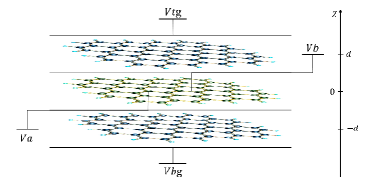
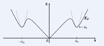
In Fig.1 we illustrate a device geometry in which flow of electron-hole pairs may be observed and in Fig.2 we sketchily represent the dispersion relation of elementary excitations in graphene multilayer device tunneling structure. We have two superconducting graphene monolayers which are separated by thin oxide barriers and one normal graphene monolayer in the middle. Top and bottom gates ( and ) are used to electrostatically. The top and bottom gates are separated manipulate the quasiparticle concentrations in the top and bottom layers. The top and bottom gates are separated from the graphene layers by gate oxides which are several nanometers thick. As the phenomenon of superfluidity of electron-hole pairs has not yet been experimentally observed in graphene multilayer structures.
A dissipationless flow of electron-hole pairs in equilibrium through the graphene mono-layer and thin oxide layers, depending on the phase difference between the two superconducting graphene layers. The single-particle Hamiltonian in graphene is the two-dimensional Dirac Hamiltonian
where acting on a four-dimensional spinor (,,,). The indices label the two sublattices of the honeycomb lattice of carbon atoms, while the indices label the two valleys of the band structure. There is an additional spin degree of freedom, which plays no role here. The 22 Pauli matrices act on the sublattice index.
The time-reversal operator interchanges the valleys
with the operator of complex conjugation. We consider a sheet of graphene in the plane. Electron and hole excitations are described by the Bogoliubov-de Gennes equation
with and the electron and hole wave functions, the excitation energy (relative to the Fermi energy ), the single-particle Hamiltonian, and the time-reversal operator. The pair potential couples time-reversed electron and hole states. In the absence of a magnetic field, the Hamiltonian is time-reversal invariant, and we yield two decoupled sets of four equations each, of the form

Separate gate electrodes make it possible to vary independently the carrier concentration of electron-hole pairs in the normal direction (-direction) to graphene mono-layer, thin oxide layers and superconducting graphene layers. For , the pair potential vanishes identically, disregarding any intrinsic superconductivity of graphene, where is a total width of graphene mono-layer and thin oxide layers. For and the superconducting graphene layers will induce a nonzero pair potential via the proximity effect similarly to what happens in a planar junction between a two-dimensional electron gas and a superconductorVolkov-1 . The bulk value for and for (with the superconducting phase) is reached at a distance from the interface which becomes negligibly small if the Fermi wavelength in superconducting layers is much smaller than the value in graphene mono-layer and thin oxide layers. We assume that the electrostatic potential in graphene mono-layer, thin oxide and superconducting graphene layers may be adjusted independently by a gate voltage or by doping. Since the zero of potential is arbitrary, we may take: for and otherwise. For large positive, and , the Fermi wave vector in graphene superconducting layers is large compared to the value in graphene mono-layer and thin oxide layers (with the energy-independent velocity in graphene).
III Specific heat
For the graphene mono-layer and oxide thin layers (where ) we assume that Fermi level is tuned to the point of zero carrier concentration. In the superconducting graphene layers there is a gap in the spectrum of magnitude .
The canonical partition function for this graphene-based structure can be interpreted as a collection of normal mode oscillators, the oscillator labelled by containing quanta of energy . First we calculate the Helmholtz free energy for normal graphene mono-layer (-like dependence) and thin oxide layers (its make dispersion relation between linear and quadratic dependence smooth, see Fig.2) which can be written as
| (1) |
where () is the largest (lowest) wavevector for which the linear dispersion is a reasonable approximation. Therefore, the contribution to free energy from the region of graphene-based structure is
| (2) |
where is the number of the component Dirac flavors, in the single layer graphene and is the Riemann zeta function. Contribution to the specific heat per unit volume is
| (3) |
III.1 Specific heat of superconducting layers: graphene-based layers
The grand potential of the system (-like dependence) is given by
| (4) |
where is the ”equilibrium” number of in the superconducting graphene layers. The summation over may be replaced by an integration, with the result
| (5) | |||||
where and are the lowest and highest values respectively of for which the quadratic approximation to the dispersion curve is reasonable (the limits of integration may be extended to ). The free energy of the -like superfluid gas is given by
| (6) |
The -like contribution to the specific heat we estimate as: , where
| (7) | |||
| (8) |

where , nm is the thickness of graphene sheet, n is the number of oxide dielectric layers (the thickness of each of them is presumed equivalent to graphene one) between normal and superconducting graphene layers. Rough low-temperature estimates often quote the result
| (9) |
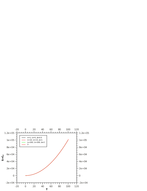
where is thermopower Scar-1 . In Fig.3 is depicted the specific heat against temperature. It is remarkable that in graphene-based superconducting structure the phonon-assisted drag effect is suppressed. The carrier concentration can be tuned varying different parameters: the thickness of oxide layers, phase difference in superconducting layers, pair and electrostatic potentials on one hand and on the another proposed structure exhibits Debye-like behaviour.
IV Conclusion
The practical significance of this investigation rests on the expectation that high-quality contacts between a superconducting graphene and normal graphene sheets can be realized. This expectation is supported by the experience with carbon nanotubes (rolled up sheets of graphene), which have been contacted succesfully by superconducting electrodes. Graphene-based structures provides a unique opportunity to explore the physics of the ”relativistic Josephson effect”, which had remained unexplored in earlier work on relativistic effects in high-temperature and heavy-fermion superconductors.
We believe that this device structure can also lead to greater understanding in another condensed matter systems such as high-temperature superconductors and exciton gases. The low cost experimental techniques allow for easy verification of the proposed hypothesis.
V ACKNOWLEDGMENT
Authors are very indebted to C. Y. Mou, E. Babaev, M. M. Parish, M. Baxendale and D. J. Dunstan for stimulating discussions and fruitful suggestions. We acknowledge Myerscough Bequest and School of Physics at Queen Mary University for financial support.
References
- (1) K. S. Novoselov, S. V. Morozov, T. M. G. Mohinddin, L. A. Ponomarenko, D. C. Elias, R. Yang, I. I. Barbolina, P. Blake, T. J. Booth, D. Jiang, J. Giesbers, E. W. Hill, and A. K. Geim, Phys. Stat. Sol. (b) 244, 4106 (2007).
- (2) M. Topsakal, H. Sevincli, and S. Ciraci, Appl. Phys. Lett. 92, 173118 (2008).
- (3) H. Sahin, R. T. Senger, and S. Ciraci, J. Appl. Phys. 108, 074301 (2010).
- (4) D. A. Areshkin, D. Gunlycke, and C. T. White, Nano Lett. 7 (1), 204 (2007).
- (5) R. R. Nair, P. Blake, J. R. Blake, R. Zan, S. Anissimova, U. Bangert, A. P. Golovanov, S. V. Morozov, A. K. Geim, K. S. Novoselov, and T. Latychevskaia, Appl. Phys. Lett. 97, 153102 (2010).
- (6) H. Sahin and R. T. Senger, Phys. Rev. B 78, 205423 (2008).
- (7) L. A. Agapito, N. Kioussis, and E. Kaxiras, Phys. Rev. B 82, 201411(R) (2010).
- (8) J. Yan, Y. Zhang, P. Kim, and A. Pinczuk, Phys. Rev. Lett. 98, 166802 (2007); H. T. Yang, arXiv:1011.3291v3.
- (9) D. Pandey, R. Reifenberger, R. Piner, Surface Science 602, 1607 (2008).
- (10) Geim, A. K., and K. S. Novoselov, Nature Matter. 6, 183 (2007).
- (11) Chen, Z., Y.-M. Lin, M. J. Rooks, and P. Avouris, Physica E 40, 228 (2007).
- (12) Nilsson, J., A. H. Castro Neto, F. Guinea, and N. M. R. Peres, Phys. Rev. B 76, 165416 (2007).
- (13) Oostinga, J. B., H. B. Heersche, X. Liu, A. Morpurgo, and L. M. K. Vandersypen, Nature Mater. 7, 151 (2008).
- (14) J. Hass, F. Varchon, J. E. Mill n-Otoya, M. Sprinkle, N. Sharma, W. A. de Heer, C. Berger, P. N. First, L. Magaud, and E. H. Conrad, Phys. Rev. Lett. 100, 125504 (2008).
- (15) Y. Sui and J. Appenzeller, Nano Lett. 9(8), 2973 (2009).
- (16) D. Bolmatov and C. Y. Mou, JETP 112, 102 (2011).
- (17) D. Bolmatova and C. Y. Mou, Physica B: Condensed Matter 405, 2896 (2010); T. Dobrowolski, Can. J. Phys. 88(9), 627-633 (2010); D. Bolmatov and C.Y. Mou, JETP 110, 612 (2010);
- (18) H. Min, R. Bistritzer, J. J. Su, and A. H. MacDonald, Phys. Rev. B 78, 121401(R) (2008).
- (19) D. V. Fil and L. Yu. Kravchenko, Low Temp. Phys. 35, 904 (2009).
- (20) L. V. Keldysh and A. N. Kozlov, Sov. Phys. JETP 27, 521 (1968).
- (21) V. W. Scarola and G. D. Mahan, Phys. Rev. B 66, 205405 (2002).
- (22) A. F. Volkov, P. H. C. Magnee, B. J. van Wees, and T. M. Klapwijk, Physica (Amsterdam) C242, 261 (1995).