The effect of changing electrode metal on solution-processed flexible titanium dioxide memristors
Abstract
Flexible solution processed memristors show different behaviour dependent on the choice of electrode material. Use of gold for both electrodes leads to switchable WORM (Write Once Read Many times) resistive devices. Use of aluminium for both electrodes increases the richness of behaviour allowing both curved and triangular memristive switching resistance memories. A comparison device with an aluminium bottom electrode and gold top electrode only exhibited significant memristive resistance switching when the aluminium electrode was the cathode, suggesting that the electrode is acting as a source/sink of oxygen anions. When the gold electrode was the cathode this electrode was deformed by oxygen evolution. These results demonstrate that aluminium is helpful for stabilising and promoting memristive behaviour in sol-gel TiO2 devices and that changing electrodes from aluminium to gold creates fundamentally different device characteristics.
Keywords: Memristor, TiO2, ReRAM, resistive switching, WORM, aluminium, gold
1 Introduction
Memristors are the fourth fundamental circuit element and have been the focus of intense research since the theory [1, 2] was recently united with a practical demonstration [3]. As they can hold a state, they may be useful as computer memory [4] and because synapses [2] can be described by the memristor theory, it is anticipated that memristor devices could operate as artificial synapses in neuromorphic computing paradigms [5] and there are several theoretical studies [6, 7, 8, 9, 10] that suggest that this approach may be fruitful and ongoing experimental projects [11, 12] (including ours) to test it out.
The definition of the memristor is a non-linear relationship between voltage and current, due to a linear relationship between charge and flux, where the memristor resistance is a function of either charge or flux [1]. In practical tests, the memristor is best identified by three ‘fingerprints’: such as the existence of a pinched hysteresis curve (specifically a Lissajous curve) [13].
In terms of technological approaches and types of materials, memristors are very similar to Resistive Random Access Memory, ReRAM (also known as RRAM). The relation between ReRAM and memristor technologies is not a settled one: it has been suggested that all resistance switching memories (include ReRAM) are memristors [14], that memristor theory can be only used to describe parts of the operation of ReRAM [15] and that some ReRAM requires an extension to memristor theory [16].
ReRAM devices are known to exhibit a rich set of behaviours including bipolar switching, BPS, a slow changing of resistance and unipolar switching, UPS, a more sudden switching regime [17]. To test for BPS, devices are subjected to a change in voltage and polarity of voltage, to test for UPS the devices are usually only tested with one voltage polarity. The results of subjecting UPS switching devices to a switch in polarity as well as voltage magnitude is not generally published and informal discussions with ReRAM scientist suggest that it’s not generally tested.
Titanium dioxide is not the only transition metal oxide that can switch via both BPS and UPS, a few examples are SrTiO3 [18, 19], NiO [20], CuO [21], ZnO [22], MnOx [23], and both binary and perovskite oxides are capable of it. The exact mechanisms are not completely understood, even if we restrict our focus to TiO2. The UPS switching has credited to: Joule heating [17], metal-semiconductor transitions [17], anion migration [17], crystalline TiO2-amorphous TiO2 phase transition via conduction heating and breaking [24], conical conducting filaments made of a Magnéli phase [25], fractal conducting filaments [26], raising and lowering Schottky barriers via bulk transport of oxygen [18], and conductance heating causing lateral transport of conducting filaments [27]. Similarly, BPS switching has been credited to: Joule heating [17], metal-semiconductor transitions [17], anion migration [17], Magnéli-insulator phase transitions [28], Ti4O7 conducting channels [29], raising and lowering Schottky barriers via interface-based transport of oxygen [18] and migration-caused slow breaking of conduction filaments [27]. There is also a debate as to what the structure of the less-conducting thin-film TiO2 is, with rutile (-TiO2) [24] and amorphous titanium dixoide (-TiO2) being the most popular suggestions. Note, that -TiO2 is also suggested as the conducting form of TiO2 and that Magnéli phases are sheer planes from -TiO2. However, the ReRAM community seems to have settled on the slow drift of vacancies or ions as being the root cause of BPS. This type of switching resembles the theoretical memristor curves and is the same mechanism as that put forward in a forthcoming theoretical paper [30]. The unipolar switching mechanism is most likely related to the creation of conducting filaments of doped material [17, 31, 24, 27, 26] and can be described by an extension to memristor theory [16]. This overlap in terms of functionality and theoretical viewpoint strongly suggest that ReRAM research is highly relevant to memristor research, a view which has been also taken up by some memristor researchers [32], thus we shall not limit ourselves to the memristor literature.
A recent paper [33] describing the creation of a solution processed TiO2 sol-gel memristor that could be fabricated on a flexible plastic substrate has attracted much interest because it could lead the way to easier fabrication of memristors as well as the possibility of flexible or wearable memristor circuitry. The archetypal memristor [3] was made with platinum electrodes which are expected to have no effect on the TiO2 switching, whereas the sol-gel memristor had aluminium electrodes [33]. There have been several examples in the ReRAM literature of aluminium oxide playing an essential role in resistance switching mechanisms [34, 35], including devices based on TiO2 and aluminium [36, 24, 37, 38], the addition of Al2O3 to improve switching [39], Al-Al2O3 resistive switching [40, 41] and even the fabrication of Al-Al2O3-Al based flexible switching memory [42]. Despite this weight of expectation that the aluminium electrodes might effect the switching in the flexible memristor, the authors did not report detailed tests and instead simply stated that the ‘switching behaviour in our devices cannot be attributed to the aluminium (or aluminium oxide), since it was also observed from devices with noble metal (gold, silver and platinum contacts’. It is known that TiO2 can switch by itself (see for example [28, 3]), but it is important to know if the aluminium electrodes are having an effect, as this would make the flexible memristor not a simpler-to-manufacture version of the Strukov memristor [3] but instead a more complex system. It is suggested that a more complex system may well have a richer set of behaviour and thus a wider range of uses.
In this paper, we have undertaken an investigation of the effect of electrode material on the TiO2 sol-gel memristor and in so doing we have discovered a much richer set of possible behaviours than has been reported previously and made an attempt to elucidate how to control which behaviour is selected. It is envisaged that this level of understanding will allow researchers to more finely control the aspects of their memristor devices and allow creation of useful and practical memristor devices.
2 Methodology
The standard memristors were prepared by first sputtering aluminium onto a plastic substrate via a mask. The sol-gel preparation is based on that found in [33, 43] and is described in detail elsewhere [44]. The final preparation was diluted 1:10 in dried methanol to make the spin-coat solution. 3ml of spin-coat solution was spun at 33 r/s for 60s and left for at least an hour (the time taken for the sol to convert to the gel [45]) before the second set of electrodes were sputtered on top. The electrodes were 4mm wide and crossed at 90 degrees giving a 16mm2 active area. Profilometer tests revealed that the TiO2 gel layer was approximately 44nm () thick.
6 batches of devices were fabricated and in total 130 devices were tested. To test the fabrication methods devices were left in clean room air to hydrolyse (R series) or put into vacuum (V series) or the top electrode size was changed to 1, 2, 3, 4 or 5mm, giving active areas of 4, 8, 12, 16 or 20mm2 (D series). The D series memristors were hydrolysed under vacuum. Comparison devices were made with: A, gold electrodes top and bottom (Au-TiO2-Au memristors); B, aluminium bottom electrodes and gold top electrode (Au-TiO2-Al memristors); and C, the standard aluminium top and bottom electrode (Al-TiO2-Al), all these devices were made with 4mm wide electrodes. From the memristor literature it is expected that the Au-TiO2-Au devices should switch similarly to the Al-TiO2-Al memristors, from the ReRAM literature it is expected that the aluminium oxide has a role to play in the switching.
Virgin memristor devices were used for all comparisons and were measured with linear I-V sweeps on a Keithley 2400 sourcemeter between a range of which is the same range as [33], with a voltage step size of 0.05V and a dwell time of 2s: this is the D.C. equivalent of an A.C. voltage of 1mHz, a frequency that it too slow to source any other way from the sourcemeter. Twelve memristors were tested in each case, the source was always connected to the bottom electrode to ensure comparability. For the Al-TiO2-Au memristor virgin runs, six devices were connected one way (Earth to Au, source to Al) and six the other way. For these devices a second run done connecting the wires the opposite way round (to reverse the asymmetry). The compliance current was 2mA unless stated.
As in [33] our electrodes were sputter coated, the TiO4(sol) is then spun on-top and hydrolyses to the gel [46]:
Ti(OH) TiO
before the next set of electrodes are sputtered on top. The Al-TiO2-Al were prepared in two different ways, depending on whether they were left in the clean room atmosphere to hydrolyse or kept under vacuum. Firstly, aluminium oxide forms very quickly and secondly the TiO2 may oxidize the bottom electrode, and so we expect the vacuum prepared memristors to have an Al2O3 layer, however it may be a different thickness or the TiO2 layer may have a different form under the two different preparation methods.
Photographs were taken with a Canon Powershot G6 using frontal and side-light from a tungsten desk lamp using a sheet of white paper as a soft-box. Micrographs were taken using on a 3D Hirox digital microscope using both frontal and side-lighting.
3 Results and Discussion
3.1 Types of Memristors Tested
3.1.1 Au-TiO2-Au Memristors
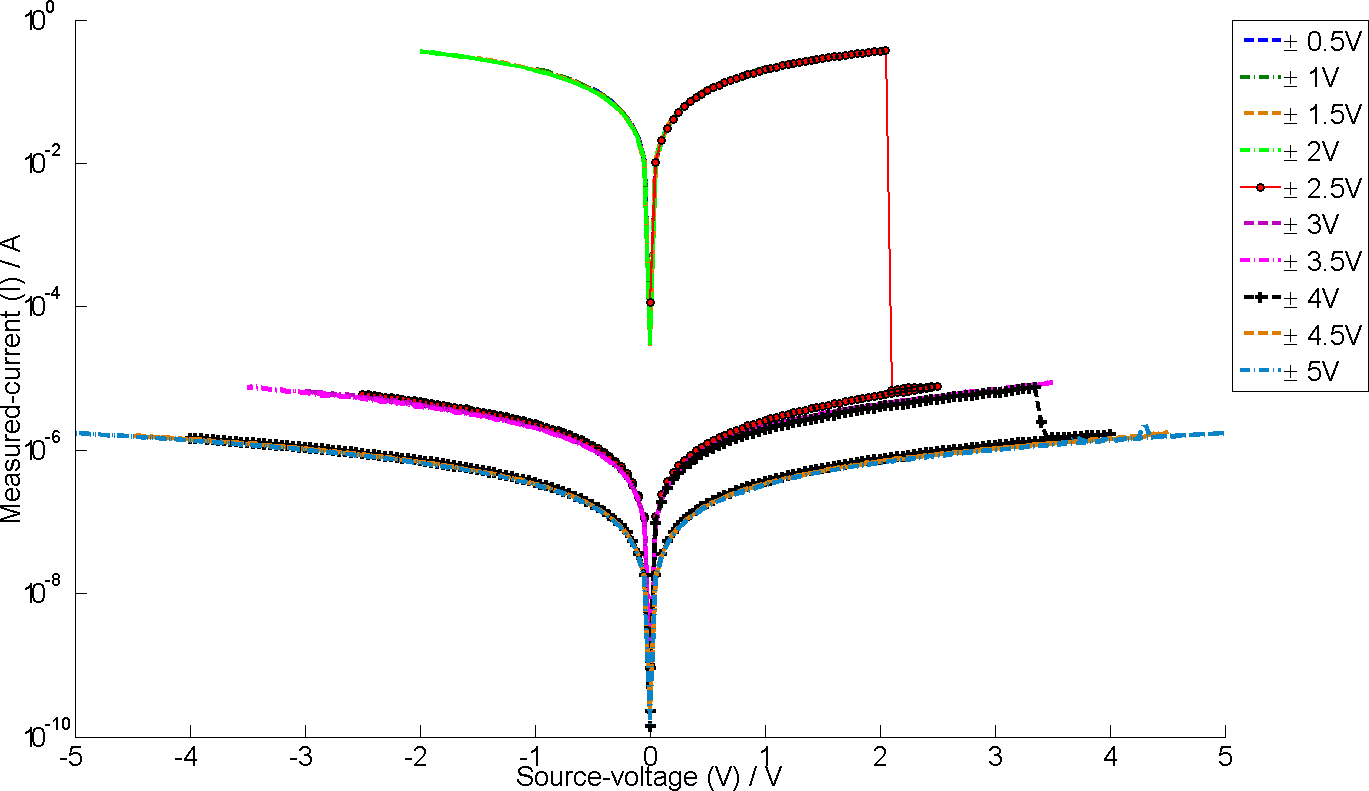
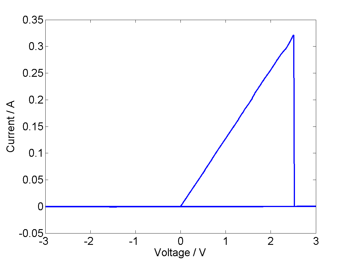
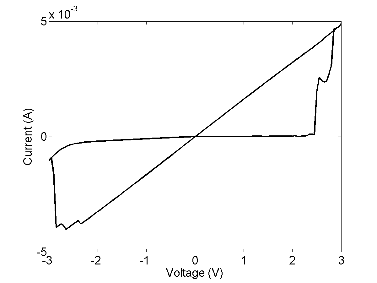
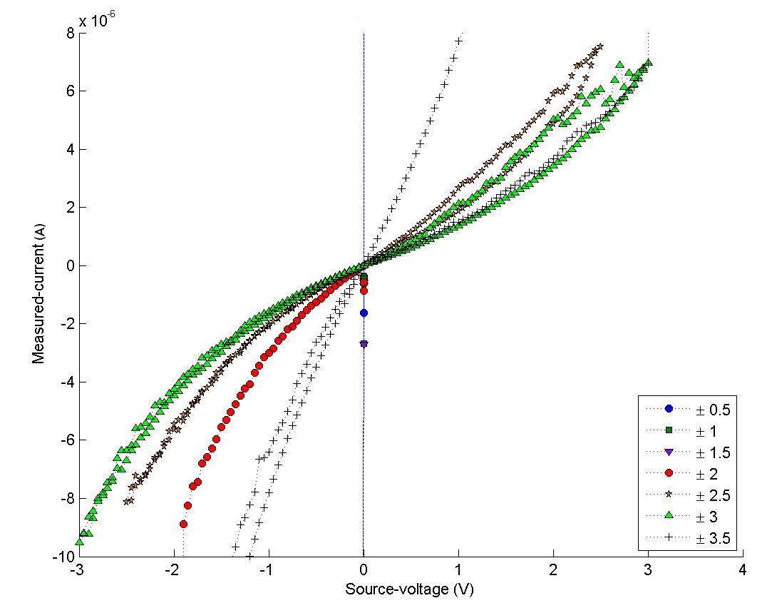
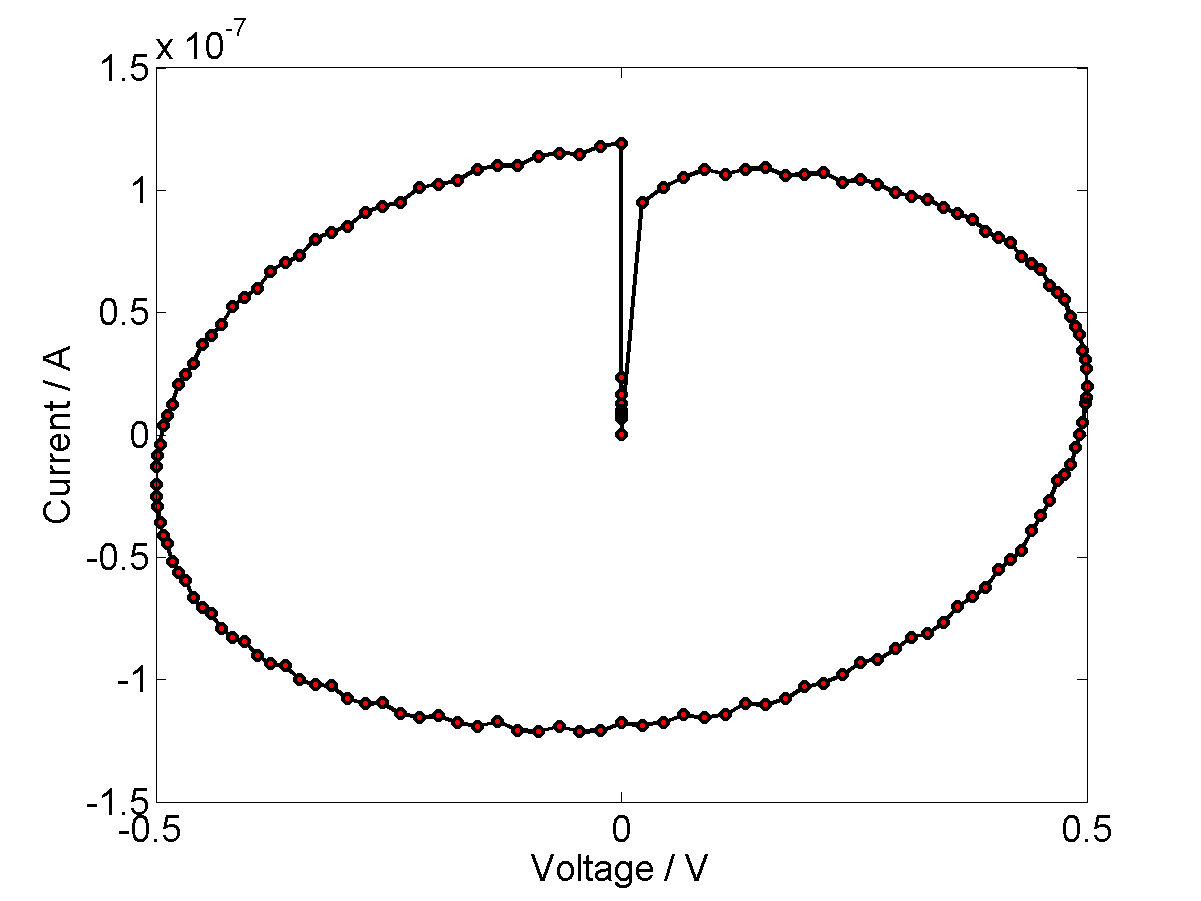
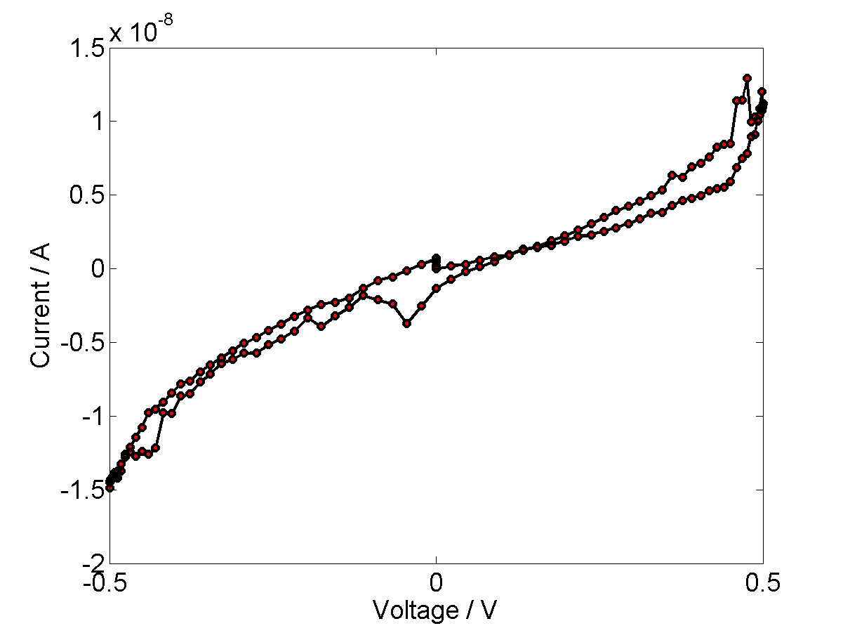
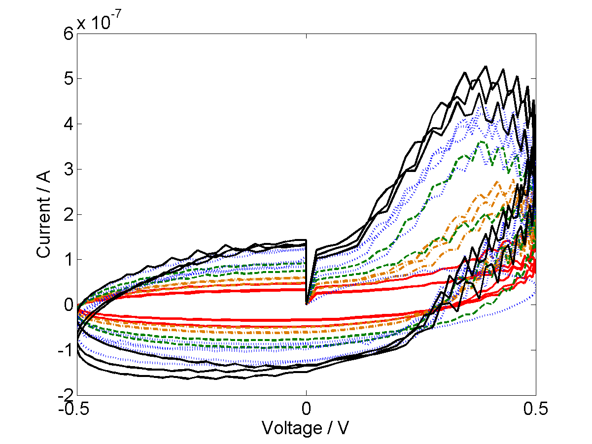
Using the gold electrodes gave a fuse-like behaviour, see figure 4A. The devices start off in a very low ohmic resistance state, see figure 2, with . This state breaks down at just over 2V to a higher resistance state, , and secondary breakdown is observed between 3 and 4V to , as shown in figure 1. This happened in all tested devices and was not reversible over a short timescale. Reversing the order that the device went round the I-V curve meant the switching behaviour was observed at a negative voltage. These devices might have applications in Write Once Read Many (times) WORM memory as the separation in current between and is in the order of 5 orders of magnitude, see figure 1. The Low Resistance State, LRS, and High Resistance State, HRS, are generally both linear and thus these devices are not memristors (they are ohmic resistance switches). We suspect that disruption of gold bridges causes the observed fall in resistance, as in [47]. A few devices showed memristive behaviour after the first fuse breaking, see for example 3, although it was not very stable, which we expect is the action of TiO2 gel.
To test for unipolarity, a device was run backwards, i.e. the negative half of the curve was run first. As would be expected if the size rather than the polarity the voltage caused the effect, the device switched on the negative side first. However, it switched at rather than , suggesting that the devices are not symmetric.
The mechanism of these devices is unknown. Silver Chalcogenide memristors operate via the reproducible formation and breaking of silver nanowires with the chalcogenide [104]. Gold is known to form nanowires which are highly extrudable (and can be used in break junctions). Filamentary conduction states have been recorded in thin continuous gold films on insulating surfaces [47]. Given these facts, and the fact that the Au-TiO2-Au device currents are much higher than the Al-TiO2-Al device currents, it could be that metallic gold filaments are forming, passing through the very thin TiO2 layer and forming a short-circuit. These filaments could then be being broken by Joule heating.
3.1.2 Al-TiO2-Al
One advantage that the sol-gel based fabrication method has over sputter or atomic deposition of TiO2 is that the sol-gel memristors can switch during their virgin I-V run and do not need a forming step. Most reported ReRAM devices require a forming step because deposited TiO2 has a very regular and crystalline structure, therefore holes or defects must be introduced [29] into the material (N.B, another approach is to add oxygen chemically during fabrication [48]) to cause appreciable conduction. The forming process generally involves pulsing [29] or increasing the voltage to high levels with a low compliance current [17, 18], this may change the device by moving the oxygen anions [29] or may change the structure via Joule heating [17] and furthermore both those statements may be equivalent in some devices, i.e., they are equivalent if Joule heating causes a structural rearrangement which moves the oxygen ions and not equivalent if the oxygen ions drift without significant heating. Forming is not necessary in the memristors reported here as the gel-form TiO2 structure is much more amorphous and already contains defects and thus these memristors can switch right away.
Behaviour and Device Properties
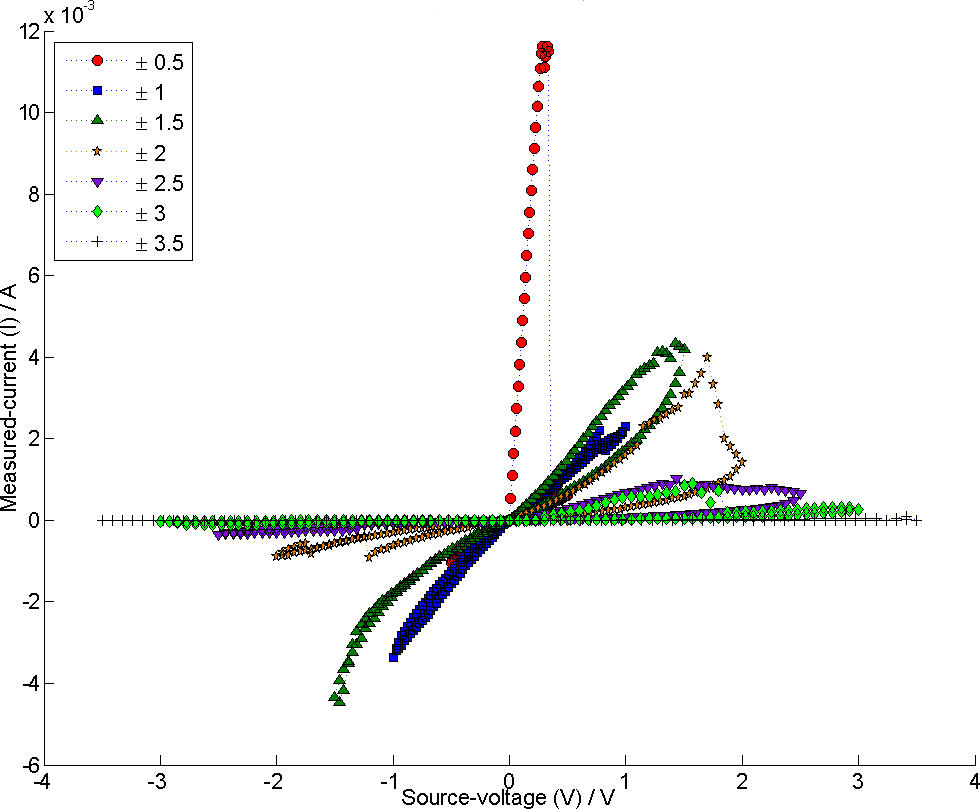
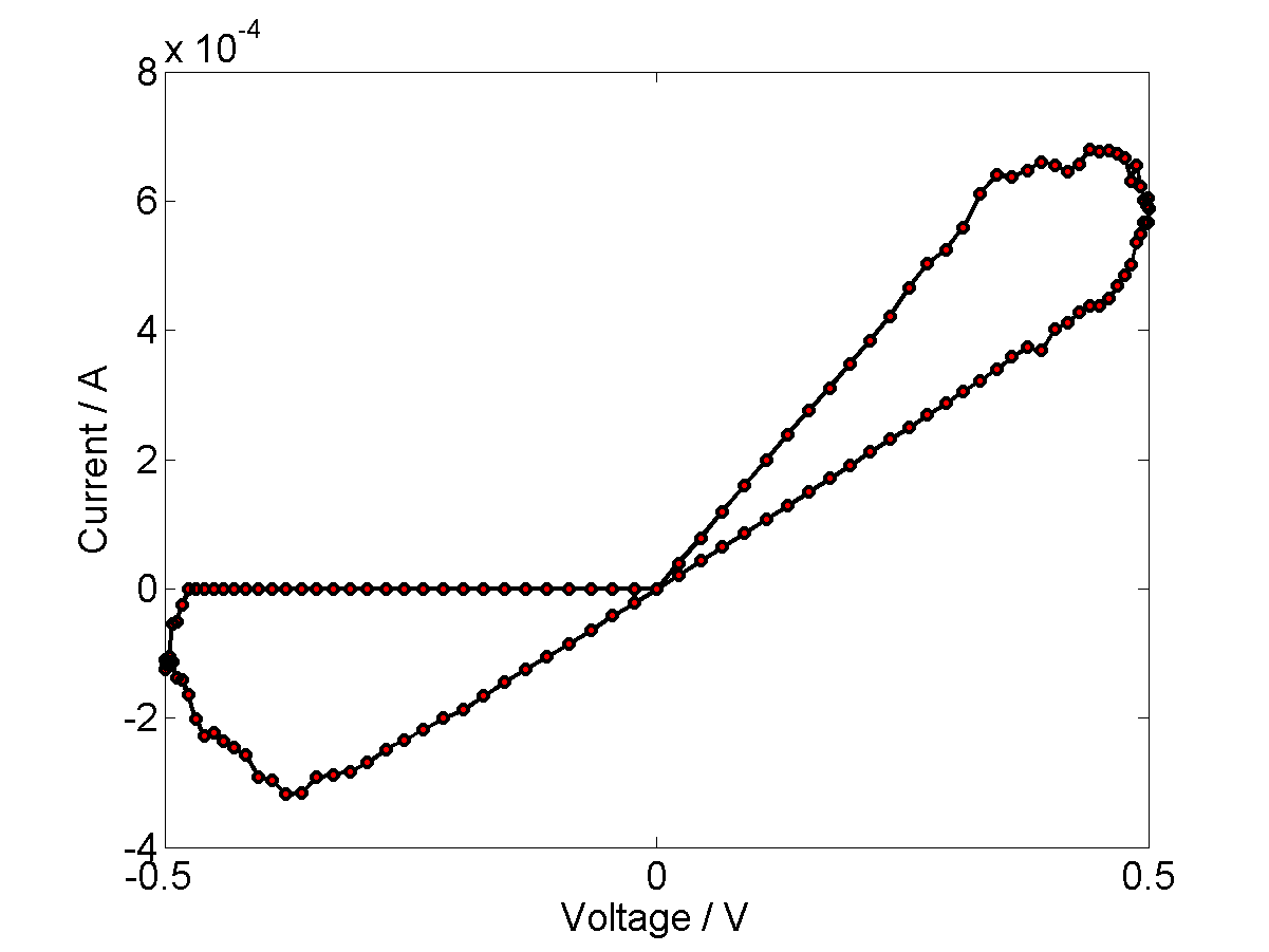
Changing both electrodes to aluminium increases the richness of the behaviour compared to gold electrode devices and improves the repeatability and stability of behaviour. We observed two types of behaviour, curved, see figure 4a and triangular, see figure 4b, I-V profiles. The curved switching profile is integrable (i.e. there are no discontinuities). These devices are very similar in form to the theoretical memristor curves [1] in that they are pinched, curved hysteresis loops, they differ in that they are more pinched close to the origin than at higher voltages. This may imply the existence of a threashold for memristive behaviour, which makes sense chemically and allows the devices to be ‘read’ at low voltages with very little or zero effect on the resistance value. Devices exhibiting this sort of switching have a HRS and LRS within the same order of magnitude which are usually in the range AA, most often around A, see figure 4a. We suggest that these devices closely resemble ReRAM BPS switching (as in [17]).
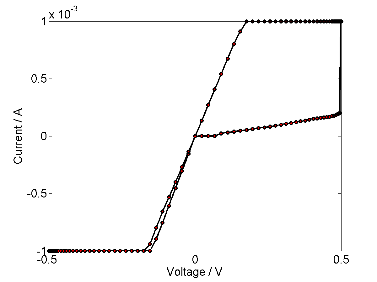
The triangular switching is shown in figure 4b. The devices start off in the HRS and then switch over a very small voltage range (i.e. there is a discontinuity in the current-time profiles) to the LRS which is orders of magnitude smaller and ohmic. The LRS gives currents in the 10-3A range and these devices never reach the 10-1 current range seen in the gold electrode devices. The HRS is curved and resembles the curved switching devices. Thus, we think the LRS is caused by filaments that connect after the device has been under a large enough voltage, and when not connected the device shows bulk memristance similar to that seen in the curved devices. These filaments give an ohmic response and could be considered as fuses. Changing the compliance current can allow a ReRAM device to switch between UPS and BPS behaviour [49], and thus we tested if changing the compliance current in these sol-gel devices would cause a transition in behaviour; it did not.
The sol-gel memristors are capable of both BPS-like and UPS-like switching. The coexistence of BPS and UPS switching has been observed before in thin-film TiO2 before [50, 24, 49], although none of these were sol-gels, and in SrTiO3 sol-gel based ReRAM [18]. The triangular-switching resembles that reported by Gergel-Hackett et al in their paper on sol-gel TiO2 memristors [33]. Our devices go round the I-V loop backwards compared to the Strukov et al memristor [3], as they start in the high conducting state and switch off, rather than the other way round. This makes sense if the gel phase is or is largely -TiO2 as it will have a high conductivity to start with, whereas the Strukov memristor is closer to a crystalline form of TiO2. Previous work using the same sol-gel solution with drop-coated devices [44] showed that the titanium dioxide gel layer was mostly the amorphous form, -TiO2.
However, our triangular switching is not necessarily UPS. Unipolar devices can be SET and RESET with only a single polarity voltage and compliance current control (as described in [49]), however this process was not found to reset these devices. A RESET to a negative voltage loop was, i.e. they are bipolar switches.
After the triangular-switching devices have been taken to a high voltage (), in subsequent I-V measurements the triangular-switching behaviour would be replaced by the curved behaviour. Once this had happened the devices were not properly reset by a negative voltage and were less reproducible: further repeated trips around the I-V curve showed a continuous memory effect whereby the HRS of one run would become the LRS of the next. This is consistent with the filament breaking leaving the memristor only operating via the bulk drift of vacancies.
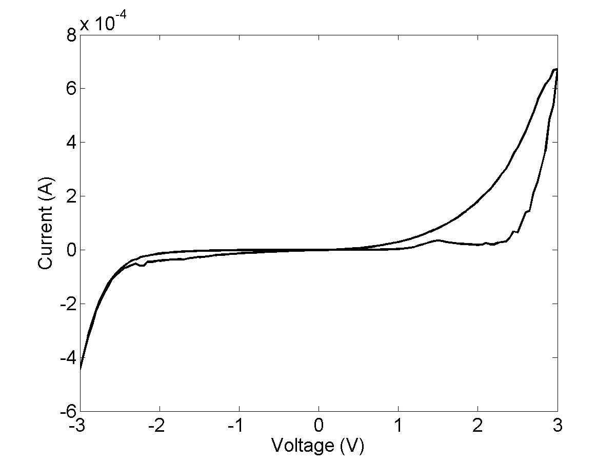
It was found that measuring an I-V curve over on virgin devices would show two types of behaviour, ohmic and a distinctive open curve as shown in figure 9e and previously reported for TiO2 thin films [50]. Devices which were ohmic over this range had starting resistances between 26 to 352 tended to exhibit triangular behaviour over higher voltage ranges, those which were curved tended to exhibit curved over a higher voltage range, providing quick device classification.
Similar devices fabricated by drop-coating the same sol-gel solution onto sputter-coated Al contacts have been tested over the same range [44] and only displayed curved switching over this voltage range. This suggests that the thickness of the layer has an effect on the presence or absence of triangular behaviour (over a given voltage range), which may suggest that the ohmic state in the triangular switching was due to the formation of filaments and the curved I-V and LRS of the triangular switching was due to unconnected filaments or background drift of oxygen vacancies.
Device Structure
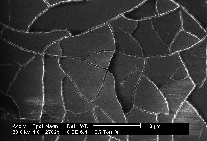
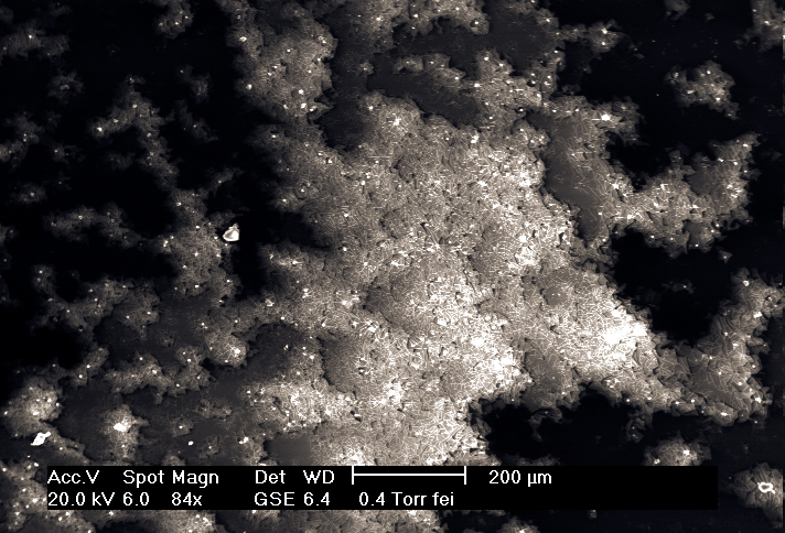
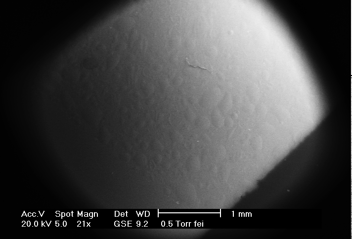
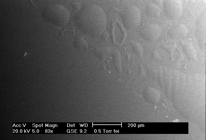
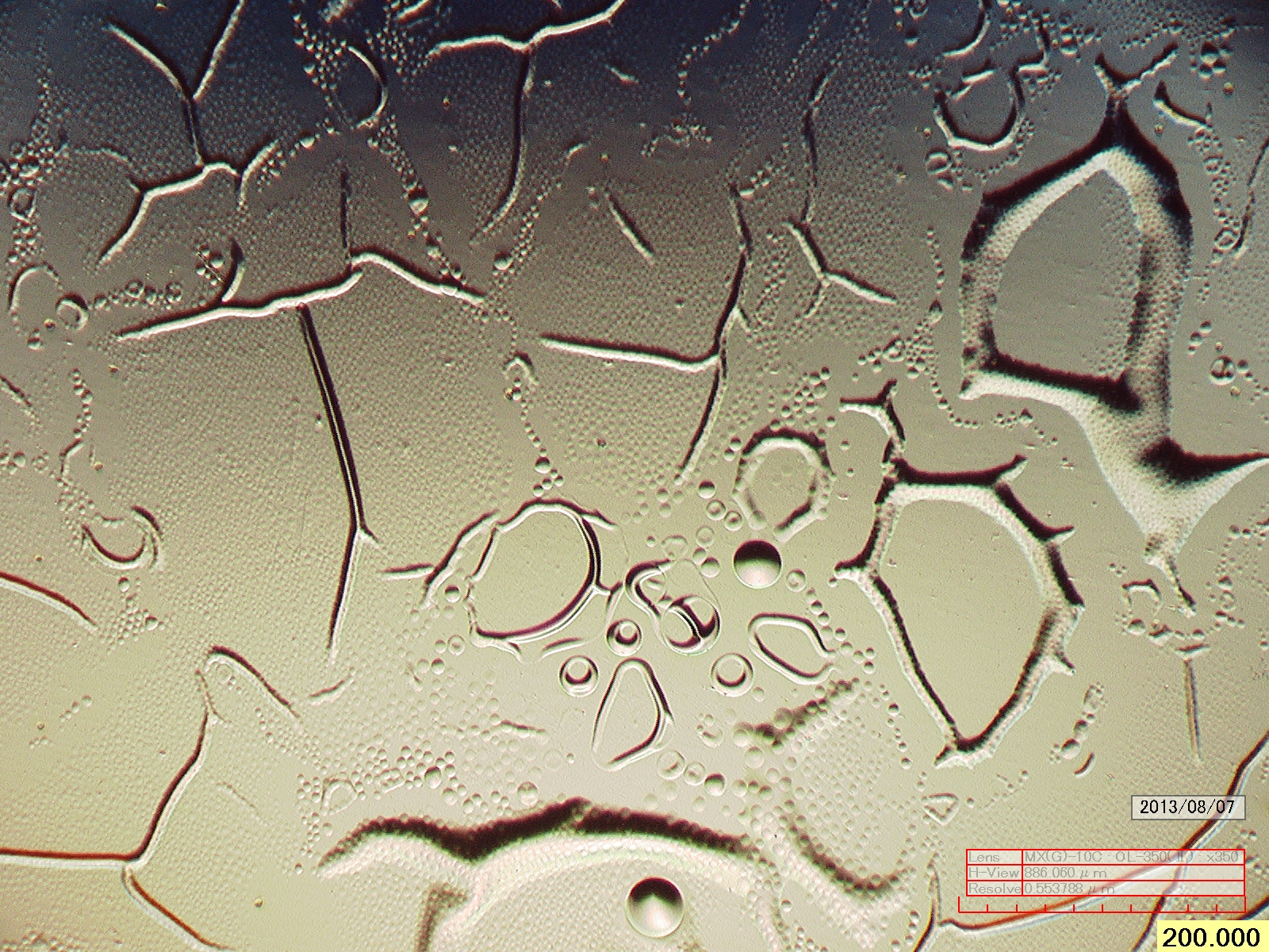
A part of the plastic covered with only TiO2 gel layer was imaged with a scanning electron microscope. Figure 5 shows the paddy-field-like structure of the surface. The ‘cracks’ were not a result of electrode beam breakage as they didn’t increase whilst the material was imaged. They could be a result of the gold sputtering required to image the surface or it could be that the flat planes are relatively regular islands of TiO2 and the ‘cracks’ are grain boundaries, the formation of extended defects along grain boundaries has been seen before [51]. Note, figure 6 shows a much wider view and we can see that the structure is like paddy-fields in that there seems to be a large difference in brightness across the sample, as the difference in brightness in a SEM micrograph is a convolution of the distance from the electron microscope tip and the electronic conductivity of the region, thus it could well be that the brighter areas are areas of more conductive TiO2 and as we know some parts of the material are in this form, we can’t rule out that they would be laterally distributed as well as distributed along the line of electron movement. Devices were sliced in half and imaged by transmission electron microscopy (TEM) and do not show obvious filaments, however, given the size of the active area and the difficulty of slicing the device more than once, absence of filaments in these micrographs does not necessarily prove their non-existence.
The Effect of Atmospheric Conditions During the TiO2 gel Formation on the Final Device Characteristics
The TiO layer was formed under two different atmospheric conditions: under vacuum overnight (V series memristors) and exposed to clean-room air overnight (R series memristors). Air humidity has been noticed to effect the qualities of memristor-like ReRAM in the past [52]. although this has not been reported with TiO2 devices. The V series were only exposed to air for a short time during transfer to from the sputterer to vacuum. The air that both memristors were exposed to was clean room air, which would have a lower proportion of water and dust than standard laboratory air. Both sets of memristors were left in their respective places overnight, giving the gel plenty of time to react.
A comparison between the two types is shown in table 1, they were tested with two different values of compliance current (c.c). It was thought that the compliance current, 2mA, would be high enough to not limit the behavioural choices of the device (as discussed earlier), however an even higher compliance current (1A), which is effectively unlimited as it is higher than any current drawn by these devices over this range, was found to change some of the behaviour. Note, that these data are four different sets of 12 memristors undergoing their virgin run, which is enough to give an indication but not enough to be statistically reliable, so the conclusions below are tentative.
In addition to curved (A) and triangular (B) designations, four others were added to the classification in table 1: ‘Mixed’ which were I-V curves that seemed to switch from triangular to curved type behaviour; ‘half-triangle’ which is a triangle in the positive I-V part of the graph qualitatively similar to that seen for Au-TiO2-Au as shown in figure 3 but with a current an order of magnitude less; ‘linear’ which an ohmic resistor I-V profile and ‘unconnected’ which is a broken device (equivalent to an open circuit). Curved and triangular types are useful as memristor devices, linear, half-triangle and mixed are only useful if they act like curved or triangular after their virgin runs (which some, but not all, do). As mixed I-V curves are only seen with the high compliance current and the sum of the number of triangular and mixed I-V curves at high c.c. is comparable to the number of triangular I-V curves at low c.c., (V), (R), we conclude that the low compliance current preserves the triangular I-V behaviour by not allowing it to break to become mixed behaviour. Similarly, from the presence of linear I-V curves at a low c.c. ((V) and (R)), a non-presence of them at the high c.c. and the presence of half-triangle I-V curves ((V) and (R)) and the similar numbers of these categories, we think that the low compliance current prevents the filaments from breaking, phenomenon which gives rise to the half-triangle designation at high compliance currents. The lower number of triangular devices with left in clean room air (R) compared to those left in vacuum at both compliance currents (5:8 and 3:5) indicates that the vacuum treatment yields much more useful devices. The number of devices exhibiting curved behaviour is not affected by either the two treatments during gel formation or the compliance current and is approximately a sixth of the tested devices.
| Types of memristors | V memristors | R memristors | ||
| Compliance current | ||||
| Memristor types seen | ||||
| Curved (Type A) | 2 | 2 | 3 | 2 |
| Triangular (Type B) | 8 | 5 | 5 | 3 |
| Mixed | 2 | 4 | ||
| Half Triangle | 2 | 3 | ||
| Linear | 2 | 4 | ||
| Not connected | 1 | |||
| Total | 12 | 12 | 12 | 12 |
The Effect of device size
64 devices were tested and 7 different device behaviours were observed with the following characteristics: 1. Ohmic: Devices were ohmic over the measurement range (0.5V) ; 2. Switch-Ohmic: Devices were ohmic over the measurement range, but switched from one ohmic value to another; 3. Jelly-bean: Devices were a pinched but open curve; 4. Circle: Devices were an open circle ; 5. Nearly UPS: Devices switched over the range but were not strictly ohmic; 6. Nearly BPS: Devices showed a pinched hysteresis loop; 7. Not connected: Devices were not connected over the range.
| Type No. | Type | No. of devices | Average Order | |
|---|---|---|---|---|
| of magnitude | ||||
| 1 | Ohmic | 24 | 3.24 | 1.27 |
| 2 | Switch Ohmic | 9 | 3.78 | 0.83 |
| 3 | Jelly Bean | 16 | 7.19 | 0.40 |
| 4 | Circle | 3 | 7.67 | 0.58 |
| 5 | Nearly UPS | 4 | 4.00 | 0.82 |
| 6 | Nearly BPS | 5 | 8.80 | 0.45 |
| 7 | Unconnected | 3 | 10.67 | 0.57 |
The Nearly UPS and Nearly BPS device designations were generally low-quality devices that switched over such a low voltage range. It was found with previous batches of devices (namely those described in the previous section) that devices which were Ohmic over 0.5V would display triangular behaviour over larger voltage ranges, and those which had open curves over this range would display curved I-V curves with large good hysteresis.
We shall group Jelly Bean, Circle and Nearly BPS types together as type A or curved behaviour and group the Ohmic, SwitchOhmic and Nearly UPS types together as Type B memristors (i.e. those which are likely to give rise to type B or triangular behaviour over larger I-V range). Thus, we have 37.5% are Type A and 57.8% of the devices are Type B (29.7% and 51.6% respectively when the Nearly BPS and UPS are excluded as Type A and Type B respectively.) compared to 16%: 83% above, where we have included linear and triangular devices in type B (the difference is due to fabrication practicalities which meant that the sol mixture was only a day old before making the devices with different electrode sizes, but a week old before making those which were subjected to different gel forming preparations). The grouping into A and B type devices is based on the device’s observed behaviour and the current range, see figure 9 and table 2 which shows that the different behaviours have different current ranges. The fact that type B devices have a HRS which is ohmic and highly conductive but an LRS which is of the same range as type A strongly suggests that type B devices work by a filament breaking and reforming mechanism and type A do not.
| Type | Type of | 1mm | 2mm | 3mm | 4mm | 5mm |
| No. | Behaviour | |||||
| 1 | Ohmic | 4 | 5 | 8 | 1 | 6 |
| 2 | Switch Ohmic | 1 | 3 | 3 | - | 3 |
| 3 | Jelly Bean | 3 | 3 | 2 | 5 | 3 |
| 4 | Circle | 1 | 1 | 1 | - | - |
| 5 | Nearly UPS | - | - | 2 | 1 | - |
| 6 | Nearly BPS | 1 | 1 | - | 1 | 1 |
| 1+2 | Group B | 50% | 61% | 68% | 12% | 69% |
| 3+4 | Group A | 40% | 30% | 19% | 62% | 23% |
| All Types | 10 | 13 | 16 | 8 | 13 |
We looked in vain for a correlation between electrode size and a favouring of one type of behaviour over another, see table 3. Essentially we generally get more of type B than type A (and here we’ve dropped the Nearly UPS and Nearly BPS from the analysis as these devices were not used for any further experiments). There is generally more type B than type A except for 4mm which was the smallest set tested (see the last line of table 3), however the R and V series which were all 4mm wide had 66.7% triangular to 16% curved, suggesting that this result is due to the non-statistical sample sizes. There is a slight increase in the type B memristors with an increase in electrode size, which makes sense as a larger active areas allows a higher probability that a filament will have formed between the electrodes, however because of the results for the 4mm case, we suggest that there is not enough evidence to conclusively suggest that there is a favouring of type B memristors over other types as the active area size is increased.
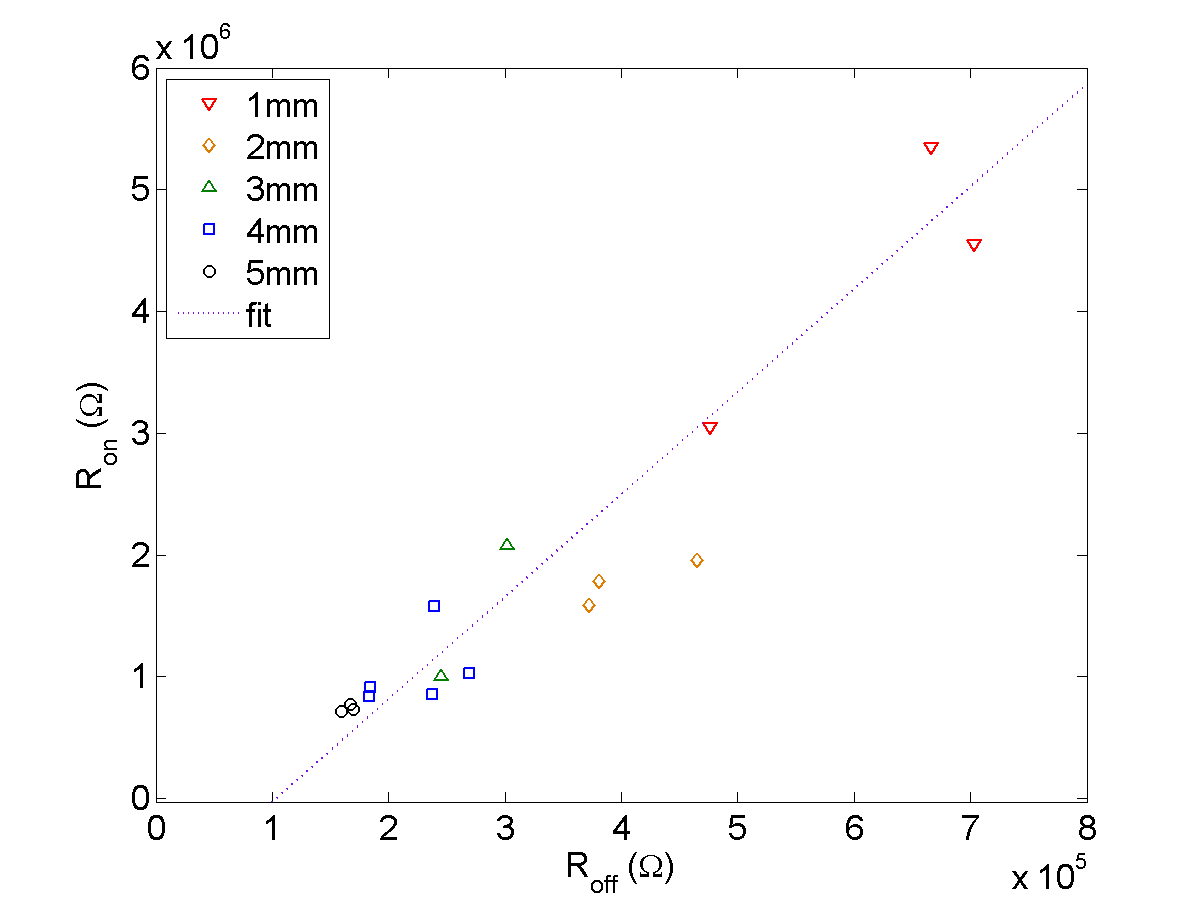
There was no correlation between where the ‘Jelly Bean’ curves cross zero and electrode width. There is a correlation between the resistance of Jelly Bean devices and the electrode width, as shown in figure 10 and figure 11. As the electrode area is increased, it makes sense that current passed should be higher if the conductance is due to a bulk mechanism. If the conduction was due to connected filaments then there would be no relation between the resistance of the device and the electrode size, and this is exactly what we see for the Ohmic or SwitchOhmic devices.
3.2 Al-TiO2-Au Memristors: The Effect of Aluminium
12 Al-TiO2-Au devices were run, 6 with the gold (top) electrode earthed, 6 with the aluminium (bottom) electrode earthed. As a comparison, the devices were run a second time with the wires switched (i.e. the aluminium electrode was earth). The virgin run did change the devices drastically, so the comparisons between virgin runs and repeated run are separated.
Aluminium Electrodes are Necessary for Appreciable Memristance
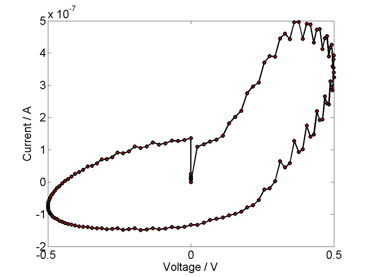
As would be expected if aluminium was essential to the operation of the flexible memristors, only one quadrant of the I-V curves showed appreciable memristance. Both types of behaviour, curved and triangular were seen. The current was in the range for curved and for triangular which is similar to Al-TiO2-Al memristors. On their virgin run memristors are very asymmetrical (as defined as no hysteresis visible on the ‘off’ side when the results are plotted over the full current range), on the second run. The ‘non-asymmetrical’ devices have some hysteresis on both sides but usually there is still visible asymmetry. The non-hysteretic part of the very asymmetrical devices was investigated to find if the hysteresis was absent or merely much smaller. When the Au electrode was earthed the currents were only on the order of 10-7-10-8A with little discernible hysteresis, when the Al electrode was earthed two things were observed, a self-crossing hysteresis in the same current as above, and, in some devices, occasional current spikes of 10-6A.
For the asymmetric virgin runs, 5/7 devices have memristance in the positive quadrant of I-V space when the Al electrode is earthed (Al is negative with respect to Au) and 6/6 have memristance in the negative quadrant when the Au electrode is earthed (Al is negative with respect to Au). Taking both virgin and second runs together, these numbers are 9/12 devices and 10/12. There is no memristance in the virgin runs when the Al electrode is positive with respect to the Au electrode. So, for appreciable memristance, the aluminium electrode has to be at a negative potential compared to the gold electrode.
3.2.1 The Electrochemistry of Au-TiO2-Al Memristors and What This Tells Us About Al-TiO2-Al Memristors
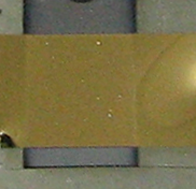
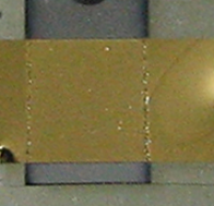
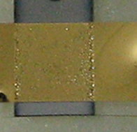
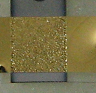
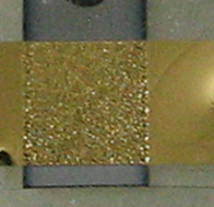
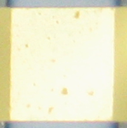
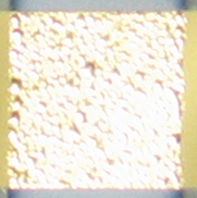
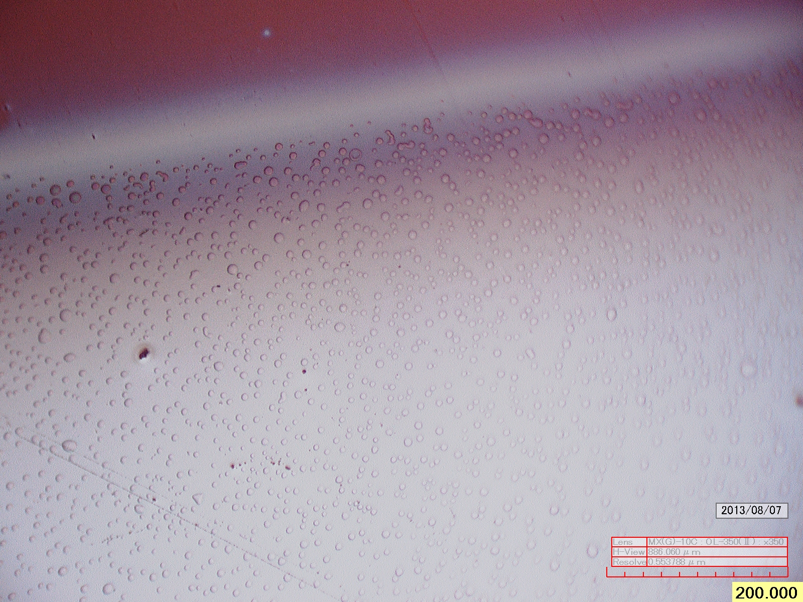
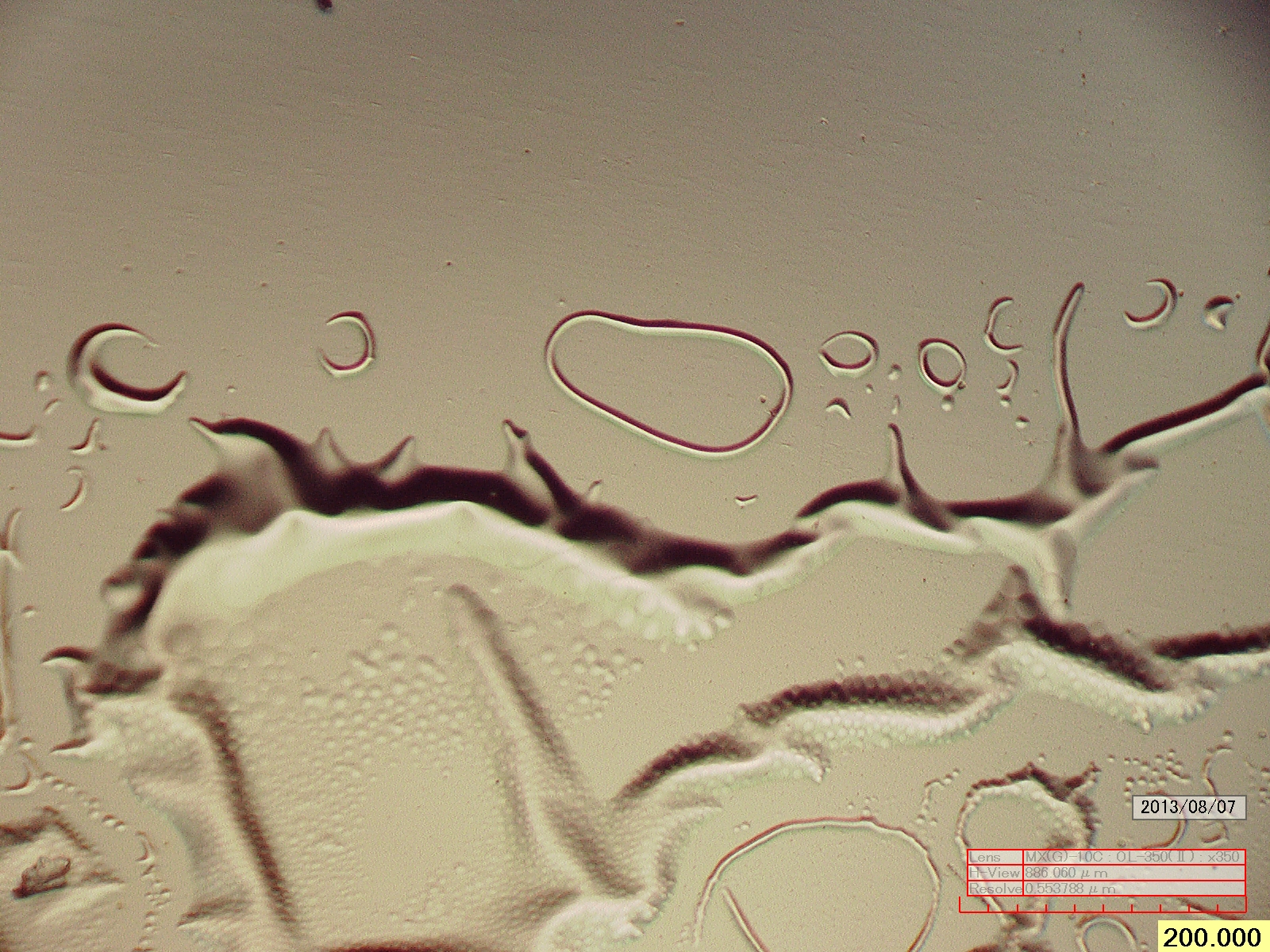
However, the Al-TiO2-Au memristor cannot simply be viewed as half a memristor, it is a different system and has different electrochemistry. It was observed that the Al-TiO2-Au devices changed in appearance after the first run (on a virgin device). It appeared as if the gold top electrode were melting and bubbling. These bubbles are shown in the SEM micrographs in figures 5 and 15. Some of the bubbles appear to have popped, see 15. The photomicrograph in figure 17 shows the sharpness of this edge.
Two devices, AlAu-12 and AlAu-14, were connected taken through virgin run I-V cycles and photographed at every time step (). As shown in figures 12 and 13. When the gold electrode of AlAu-12 was earthed the transition from a smooth surface to a bubbled one happens at +1.5V (), when the Au electrode is -1.5V with respect to the Aluminium electrode. For AlAu-14, when the aluminium electrode is earthed, the transition happens at -1.5V, again the Au electrode is negative with respect to the aluminium electrode. Note, this is the opposite way round to the appreciable memristance. In other words, if the Al is negative compared to Au we will usually see appreciable hysteresis, if the Au is negative with respect to the Al (the other half of the I-V curve), we will see very little hysteresis and instead the gold surface will deform. There is no feature in the I-V curve associated with this surface deformation at (thus far we’ve always taken the source as being connected to the bottom electrode, following this schema the deformation happens in the positive quadrant of the I-V curve).
Both sets of photographs were lit slightly differently, AlAu-12 was side-lit with glancing light which serves to show up the 3-D structure of the surface, see figure 12, AlAu-14 was directly lit which makes the photos brighter and was strong enough light to allow us to see through the gold electrode film 13. AlAu-14 shows a change in structure at -1.4V before the surface bubbles are observed. This disturbance starts in the centre of the active area, but in both AlAu-12 and AlAu-14 the deformation of the gold electrode starts at the edge of the active area, where the top electrode would be under the largest mechanical stress. The light source was not moved during the photography and thus a very simple analysis of the photographs was possible. The photographs were in aligned in Photoshop and cropped to region shown in figure 13. These photographs were read into MatLab and the column brightness was averaged in each frame (similar results were seen when the row brightness was averaged). The blue channel was chosen to analyse as blue is the complimentary colour of yellow, the main hue of gold and thus the effect was more visible in this channel (NB. the file was in RGB format). Qualitatively similar but quantitatively smaller effects were seen in the red and green channels (yellow is a mix of red and green in this colourspace). The effect of this simple analysis matches what is seen with the eye, but adds two facts: the -1.4V change, coloured in blue happens between pixels 20 and 180 (this is inside the active area) and then the change in surface texture happens quickly and then stays relatively constant. Due to this irreversible change in electrode structure, Al-TiO2-Au devices are not considered to be reproducible or particularly useful. Given the high availability costs of fabrication and uselessness as devices, the reverse (gold bottom electrode and aluminium top electrode) devices were not investigated.
This observed physical effect (bubble) can give information about the mechanism and structure of the memristors. Oxygen evolution has been observed in ReRAM, but not in gel-form TiO2 memristors. Both the memristor and ReRAM communities agree that the resistance switching/memristance happens when the titanium dioxide is reduced from the stoichiometric TiO2 form to an oxygen-deficient form TiO(2-x). TiO2 is a semi-conductor. TiO(2-x) can be thought of as either have more free electrons (the electrochemist’s viewpoint) or as having positive holes (the semiconductor physicist’s viewpoint) or oxygen vacancies (the crystallographic chemist’s viewpoint). Regardless of terminology, the reduced form of titanium dioxide is more conductive . There is debate about the exact form of the reduced form titanium dioxide (i.e. what the number is), it was thought to be a Rutile-based phase, but Magnéli phases have recently been implicated (see Introduction).
The electrochemical mechanism, as taken from [17], is as follows. The oxygen anions move under the effect of voltage (this is equivalent to the drift of oxygen vacancies mentioned in [30]). Ti cations trap electrons emitted from the cathode thus:
and there is oxidation at the anode (as this is where the oxygen anions are moving towards), possibly something like this,
If the anode is gold or another noble metal, i.e. one that cannot form an oxide, we would get
at the anode, where is understood to be an oxygen vacancy in the TiO2(of charge 2). ( is the evolution of oxygen gas). As the gold is thin and malleable enough to deform, oxygen gas evolution would explain the gold electrode deformation.
When we reverse the voltage polarity, i.e. when aluminium is the anode, we see no obvious gas evolution, no visible electrode deformation and memristive hysteresis in the I-V curve. This strongly suggests that the aluminium electrode is acting as a sink of oxygen anions. It is possible that in the Al-TiO2-Al devices when the voltage direction is switched, the aluminium oxide layer is capable of acting as a source of oxygen anions. It is suggestive that the Al-TiO2-Al devices are reproducible, in that they can be taken around the I-V curve several times, and the Al-TiO2-Au devices are destroyed after the first run.
After observation of this electrode deformation effect for Au-TiO2-Al memristors we put the Al-TiO2 electrodes under the microscope. It had been observed by eye that the Al-TiO2-Al memristors do look slightly cloudier after their virgin runs. Figure 16 shows a comparison for the gold surface electrode (actually device AlAu-14) compared to an aluminium top electrode from a Al-TiO2-Al device (V series). Although the top electrode is deformed after it’s virgin run, the size of the bubbles is much smaller, specifically no larger around 11m, whereas the bubble in figure 17 is 556.25m on its largest diameter.
 |
 |
 |
 |
 |
 |
 |
 |
 |
| -1.3V | -1.4V | -1.5V | -1.6V |
4 Conclusion
| Aluminium | Gold | ||||
| V series | R series | Al-TiO2-Au | |||
| Aluminium | UPS-like | 5 | 3 | UPS-like | 6 |
| BPS | 2 | 2 | BPS | 2 | |
| Mixed (BPS&UPS) | 2 | 4 | Mixed (BPS&UPS) | 1 | |
| Mixed (HT&BPS) | 2 | ||||
| Half-triangle | 2 | 3 | Half-triangle | 1 | |
| Total | 12 | 12 | Total | 12 | |
| Au-TiO2-Au | |||||
| BPS | |||||
| Gold | UPS-like | ||||
| BPS | |||||
| Mixed (BPS&UPS) | |||||
| Mixed (HT&BPS) | |||||
| Half-triangle | 6 | ||||
| Total | 6 | ||||
In order to elucidate how to control memristor electronic properties we have undertaken a study of several variable fabrication parameters, namely electrode material, humidity during gel formation and electrode size, and one variable measurement/forming parameter, namely the compliance current.
We have found that using gold electrodes instead of aluminium does not give good memristor devices, instead we get ohmic low resistance resistors consistent with gold metal filaments, which may fuse to lower resistance resistors usable for WORMS memory or may switch to low-quality curved type A memristor behaviour consistent with the TiO2 gel layer switching.
Mixed electrode devices with an aluminium bottom electrode and a gold top electrode seem to suffer from oxygen evolution when gold is the anode and memristance when aluminium is the anode, suggesting that the aluminium or aluminium oxide layer on the electrode is involved in supporting memristance in flexible TiO2 devices. These devices are useless as memristors or memory.
Aluminium electrode devices (Al-TiO2-Al) offer a richer behaviour which we have classified into two types. Type A or curved behaviour is explainable using fundamental memristor theory, specifically they are non-transversal memristors (see [13]) when measured at low voltages and appear to be transversal memristors when measured at larger voltages. Type A behaviour is also describable as ReRAM BPS. Changing humidity during sol formation, compliance current or electrode size does not increase the number of type A behaviour. The resistance of type A memristors can be reduced by increasing the electrode size which is consistent with type A behaviour being due to a bulk motion of oxygen vacancies. Although not presented here, we have found that type A memristors tend to be more reproducible on repeated runs and are useful for building neuromorphic circuits, logic gates and as memristors.
Type B or triangular behaviour seems similar to ReRAM UPS behaviour, although as ReRAM researchers rarely subject their UPS devices to a bipolar voltage waveform as we have here we can’t be sure. Technically type B behaviour does not fit the strict definition for the memristor [1, 2] because the resistance of the LRS is not non-linear. This fact, taken with the facts that the resistance of the LRS state is not related to the size of the electrode strongly suggests that the LRS is due to a filament which forms and is then broken and reformed (a fuse, anti-fuse mechanism). We can’t definitively conclude here that the filament is due to oxygen vacancy motion and not a titanium cation wire, however the existence of gas evolution bubbles suggests that this is the case. As the LRS state is curved it suggests that type A behaviour is there alongside type B behaviour, in that the effects of the bulk movement of oxygen vacancies is drowned out by the large ohmic current until the filament breaks. This is supported by the mixed devices which switch the type A behaviour after the filament breaks. Extending the basic memristor theory to include a filament would allow the device to be described by memristor-based equations. Taking a wider definition of memristance such as that described in [14] includes these devices as memristive systems. To get the largest number type B devices we want to allow our gel to form under vacuum and use a compliance current to prevent irreversible anti-fusing. Although not presented here, we have found that type B devices are less reproducible on repeated runs (as the filament does not break at exactly the same voltage it breaks at during the virgin run, which is consistent with results for ReRAM UPS), and seem to be useful as memory or as neuromorphic circuits.
References
References
- [1] L. O. Chua. Memristor - the missing circuit element. IEEE Trans. Circuit Theory, 18:507–519, 1971.
- [2] Leon O. Chua and Sung Mo Kang. Memristive devices and systems. Proceedings of the IEEE, 64:209–223, 1976.
- [3] D. B. Strukov, G. S. Snider, D. R. Stewart, and R. S. Williams. The missing memristor found. Nature, 453:80–83, 2008.
- [4] J. M. Tour and T. He. The fourth element. Nature, 453:42–43, 2008.
- [5] Greg S. Snider. Spike-timing-dependent learning in memristive nanodevices.
- [6] Sung Hyun Jo, Ting Chang, Idongesit Ebong, Bhavitavya B. Bhadviya, Pinaki Mazumder, and Wei Lu. Nanoscale memristor device as a synapse in neuromorphic systems. Nanoletters, 10:1297–1301, 2010.
- [7] Bernabé Linares-Barranco and Teresa Serrano-Gotarredona. Memristance can explain spike-time dependent plasticity in neural synapses. Nature Precedings.
- [8] D. Howard, E. Gale, L. Bull, B. De Lacy Costello, and A. Adamatzky. Evolution of plastic learning in spiking networks via memristive connections. IEEE Transactions on Evolutionary Computation, 16:711–729, 2012.
- [9] Gerard David Howard, Ella Gale, Larry Bull, Benjamin de Lacy Costello, and Andrew Adamatzky. Evolving spiking networks with variable memristors. In Proceedings of the 13th annual conference on Genetic and evolutionary computation, GECCO ’11, pages 1275–1282, New York, NY, USA, 2011. ACM.
- [10] G. Howard, E. Gale, L. Bull, B. de Lacy Costello, and A. Adamatzky. Towards evolving spiking networks with memristive synapses. In Artificial Life (ALIFE), 2011 IEEE Symposium on, pages 14 –21, april 2011.
- [11] Greg Snider, Rick Amerson, Dick Carter, Hisham Abdalla, Muhammad Shakeel Qureshi, Jasmin Leveille, Massimiliano Versace, Heather Ames, Sean Patrick, Benjamin Chandler, Anatoli Gorchetchnikov, and Ennio Mingolla. From synapses to circuitry: Using memristive memory to explore the electronic brain. Computer, pages 21–28, Feb 2011.
- [12] Jeyavijayan Rajendran, Harika Maenm, Ramesh Karri, and Garrett S. Rose. An approach to tolerate process related variations in memristor-based applications. In VLSI Design (VLSI Design), 2011 24th International Conference on, pages 18 –23, jan. 2011.
- [13] C.A. Lütken S. Grimes and O.G. Martinsen. Memristive properties of human sweat ducts. World Congress on Medical Physics and Biomedial Engineering, 25/7:696–698, 2009.
- [14] Leon Chua. Resistance switching memories are memristors. Applied Physics A: Materials Science & Processing, pages 765–782, 2011.
- [15] Rainer Waser, editor. Nanoelectronics and Information Technology. Wiley-VCH, third edition, 2002.
- [16] Ella M Gale, Benjamin de Lacy Costello, and Andy Adamatzky. Filamentary extension of the Mem-Con theory of memristance and its application to titanium dioxide Sol-Gel memristors. In 2012 IEEE International Conference on Electronics Design, Systems and Applications (ICEDSA 2012), Kuala Lumpur, Malaysia, November 2012.
- [17] Rainer Wasser and Masakazu Aono. Nanoionics-based resistive switching memories. Nature Materials, 6:833–840, 2007.
- [18] M.H. Tang, Z.P. Wang, J.C. Li, Z.Q.Zeng, X.L. Xu, G.Y. Wang, L.B. Zhang, Y.G. Xiao, S.B. Yang, B. Jiang, and J. He. Bipolar and unipolar resistive switching behaviors of sol-gel-derived srtio3 thin films with different compliance currents. Semiconductor Science and Technology, 26:075019 (4pp), 2011.
- [19] Xianwen Sun, Guoqiang Li, Xin’an Zhang, Linghong Ding, and Weifeng Zhang. Coexistence of the bipolar and unipolar resistive switching behaviours in au/sttio3/pt cells. Journal of Physics D: Applied Physics, 44:125404 (5pp), 2011.
- [20] L. Goux, J.G. Lisoni, M. Jruczak, D.J. Wouters, L. Courtade, and Ch. Muller. Coexistence of bipolar and unipolar resistive-switching modes in nio cells made by thermal oxidation of ni layers. Journal of Applied Physics, 107:024512, 2010.
- [21] R. Yasuhara, K. Fujiwara, K. Horiba, H. Kumigashira, and M. Kotsugi. Inhomogeneous chemical states in resistance-switching devices with a planar-type pt/cuo/pt structure. Applied Physics Letters, 95:012110, 2009.
- [22] Wen-Yuan Chang, Yen-Chao Lai, Tai-Bor Wu, Sea-Fue Wang, Frederick Chen, and Ming-Jinn Tsai. Unipolar resistive switching characteristics of zno thin films for nonvolatile memory applications. Applied Physics Letters, 92:022110, 2008.
- [23] Sen Zhang, Shibing Long, Weihua Guan, Qi Liu, Qin Wang, and Ming Liu. Resistive switching characteristics of mnox-based reram. Journal of Physics D: Applied Physics, 42:055112, 2009.
- [24] B.J. Choi, D.S. Jeong, S.K. Kim, C.Rohde, S. Choi, J.H. Oh, H.J. Kim, C.S. Hwang, K. Szot, R. Waser, B. Reichenberg, and S. Tiedke. Resistive switching mechanism of tio2 thin films grown by atomic-layer deposition. Journal of Applied Physics, 98:033715, 2005.
- [25] Deok-Hwang Kwon, Kyung Min Kim, Jae Hyuck Jang, Jong Meyong Jeon, Min Hwan Lee, Gun Hwan Kim, Xiang-Shu Li, Gyeong-Su Park, Bora Lee, Seungwu Han, Miyoung Kim, and Cheol Seong Hwang. Atomic structure of conducting nanofilaments in tio2 resistive switching memory. Nature Nanotechnology, 5:148–153, 2010.
- [26] J.S. Lee, S.B. Lee, S.H. Chang, L.G. Gao, B.S. Kang, M.-L. Lee, C.J. Kim, T.W. Noh, and B. Kahng. Scaling theory for unipilar resistance switching. Physical Review Letters, 105:205701–1:205701–4, 2010.
- [27] Daniele Ielmini, Federico Nardi, and Carlo Cagli. Universal reset characteristics of unipolar and bipolar metal-oxide rram. IEEE Transactions on Electron Devices, 58:3246–3253, 2011.
- [28] K. Szot, M. Rogala, W. Speier, Z. Klusek, A. Besmehn, and R. Waser. TiO2 - a prototypical memristive material. Nanotechnology, 22:254001–1 – 254001–21, June 2011.
- [29] A.M. Bratkovsky S.E. Savel’ev, A.S. Alexandrov and R. Stanley Williams. Molecular dynamics simulations of oxide memory resistors (memristors). Nanotechnology, 22:254011, 2011.
- [30] Ella Gale. The missing memristor magnetic flux found. Submitted, pre-print at http://arxiv.org/abs/1106.3170v2, Submitted 2013.
- [31] D. H. Kwon, J. M. Jeon, J. H. Jang, K.M. Kim, C.S. Hwang, and M. Kim. Direct observation of conducting paths in tio2 thin film by transmission electron microscopy. Microsc Microanal, 2009.
- [32] Nadine Gergel-Hackett, Joseph L. Tedesco, and Curt A. Richter. Memristors with flexable electronic applications. Proceedings of the IEEE, 2011.
- [33] Nadine Gergel-Hackett, Behrang Hamadani, Barbara Dunlap, John Suehle, Curt Richer, Christina Hacker, and David Gundlach. A flexible solution-processed memrister. IEEE Electron Device Letters, 30:706–708, 2009.
- [34] Kever T, U. Bottger, C. Schlindler, and R. Waser. On the origin if bistable resistive switching in metal organic charge transfer complex memory cells. Applied Physics Letters, 91:083506, 2007.
- [35] Micheal Colle, Michael Buchel, and Dago M. de Leeuw. Switching and filamentary conduction in non-volatile organic memories. Organic Electronics, 7:305–312, 2006.
- [36] Hu Young Jeong, Jeong Yong Lee, Sung-Yool Choi, and Jeong Won Kim. Microscopic origin of bipolar resistive switching of nanocale titanium oxide thin films. Applied Physics Letters, 95:162108, 2009.
- [37] Jeong Yong Lee Hu Young Jeong and Sung-Yool Choi. Interface-engineered amorphous tio2 based resistive memory devices. Advanced Functional Materials, 20:3912–3917, 2010.
- [38] Jing Wu, Ken Mobley, and Richard L. McCreery. Electronic characteristics of fluorene / tio2 molecular heterojunctions. The Journal of Chemical Physics, 126:024704, 2007.
- [39] Frank Verbakel, Stefan C. Meskers, Rene A. Janssen, Henrique L. Gomes, and Micheal Colle. Reproducable resistive switching in nonvolatile organic memories. Applied Physics Letters, 91:192103, 2007.
- [40] W. Zhu, T.P. Chen, Z. Liu, Y. Liu M. Yang, and S.H.Y. Fung. Resistive switching in aluminium/anodized aluminium film structure without forming process. Journal of Applied Physics, 106:093706, 2009.
- [41] Sungho Kim and Yang-Kyu Choi. Resistive switching of aluminium oxide for flexible memory. Applied Physics Letters, 92:223508, 2008.
- [42] Sungho Kim and Yang-Kyu Choi. Resistive switching of aluminium oxide for flexible memory. Applied Physics Letters, 92:223508, 2008.
- [43] Sung Heum Park, Anshuman Roy, Serge Beaupre, Shinuk Cho, Nelson Coates, Ji Sun Moon, Daniel Moses, Mario Leclerc, Kwanghee Lee, and Alan J. Heeger. Bulk heterojunction solar cells with internal quantum efficiency approaching 100%. Nature Photonics, 2009. Used methodology in supplimentary material.
- [44] Ella Gale, Richard Mayne, Andrew Adamatzky, and Ben de Lacy Costello. Drop-coated titanium dioxide memristors. Materials Chemistry and Physics, 143:524–529, January 2014.
- [45] Jin Young Kim, Sun Hee Kim, Hyun-Ho Lee, Kwanghee Lee, Wanli Ma, Xiong Gon, and Alan J. Heeger. New architecture for high-efficiency polymer photovoltaic cells using solution-based titanium oxide as an optical spacer. Advanced Materials, 18:572–576, 2006.
- [46] E.M. Drakakis, S.N. Yaliraki, and M. Barahona. Memristors and bernoulli dynamics. 2010 12th International Workshop on Cellular Nanoscale Networks and their Applications (CNNA), 2010.
- [47] R. Blessing and H. Pagnia. Forming process, i-v characteristics and switching in gold island films. Thin Solid Films, 52:333–341, 1978.
- [48] T. Prodromakis, K. Michelakis, and C. Toumazou. Fabrication and electrical characteristics of memristors with tio2/tio2 active layers. In Circuits and Systems (ISCAS), Proceedings of 2010 IEEE International Symposium on, pages 1520 –1522, 30 2010-june 2 2010.
- [49] Doo Seok Jeong, Herbert Schroeder, and Rainer Waser. Coexistence of bipolar and unipolar resistive switching behaviors in a Pt/TiO2/Pt stack. Electrochemical and Solid State Letters, 10:G51–G53, 2007.
- [50] F. Argall. Switching phenomena in titanium oxide thin films. Solid State Electronics, 11:535–541, 1968.
- [51] K. Szot, W. Speier, R. Carius, U. Zastrow, and W. Beyer. Localized metallic conductivity and self-healing during thermal reduction of SrTiO3. Physical Review Letters, 88:075508–1 – 075508–3, 2002.
- [52] J. C. Bernede. Polarized memory switching in mis thin films. Thin Solid Films, 81:155–160, 1981.