Graphing and Grafting Graphene: Classifying Finite Topological Defects
Abstract
The structure of finite-area topological defects in graphene is described in terms of both the direct honeycomb lattice and its dual triangular lattice. Such defects are equivalent to cutting out a patch of graphene and replacing it with a different patch with the same number of dangling bonds. An important subset of these defects, bound by a closed loop of alternating 5- and 7-membered carbon rings, explains most finite-area topological defects that have been experimentally observed. Previously unidentified defects seen in scanning tunneling microscope (STM) images of graphene grown on SiC are identified as isolated divacancies or divacancy clusters.
Producing commercial graphene-based devices will require the ability to grow large sheets of high-quality graphene. Several techniques for producing graphene exist, including mechanical exfoliation from graphiteNovoselov et al. (2005), chemical exfoliation from graphiteHernandez et al. (2008), chemical reduction of graphene oxideStankovich et al. (2007), segregation of carbon from metal crystalsYu et al. (2008), chemical vapor deposition of C onto metal surfacesKim et al. (2009); Li et al. (2009), and thermal desorption of Si from SiCRutter et al. (2007); Kedzierski et al. (2008). Graphene produced by the above methods is often found to contain defects, such as vacanciesUgeda et al. (2010) or grain boundariesCoraux et al. (2008); Wofford et al. (2010); Huang et al. (2011). Defects decrease the high mobility of grapheneChen et al. (2009); therefore, it is desirable to reduce or eliminate the number of defects. Conversely, one may desire to tune the properties of graphitic materials, e.g. the bandgap, by intentionally creating and manipulating defect structuresLusk and Carr (2008); Lahiri et al. (2010); Lusk et al. (2010); Terrones et al. (2010). Toward either end, it is necessary to classify the kinds of defects that form in graphene and to correlate them with the growth conditions.
One class of defects, frequently observed in scanning tunneling microscope (STM) images of ultrahigh-vacuum graphene growth via Si desorption from SiCRutter et al. (2007); Guisinger et al. (2008), exhibits regions, roughly several nm in size, of strongly perturbed electronic structure completely surrounded by ordered graphene. The finite range of the electronic structure perturbation suggests that these defects could be created or healed by the motion of a relatively small numbers of atoms, and may therefore be among the most important defects in graphene. We recently identifiedCockayne et al. (2011) the sixfold symmetric defect seen in Ref. Rutter et al., 2007 as the “flower” defectPark et al. (2010); Meyer et al. (2011) (shown below), a topological defect that can be described as the rotation of 24 central atoms in ideal graphene by 30∘. Other finite-area defects, with twofold, and threefold symmetry, are seen in Ref. Rutter et al., 2007, but their structures have not been previously identifiedGuisinger et al. (2008). In this paper, we describe a systematic procedure for describing and investigating finite-area topological defects, and, through this method, identify several of these “new” defects as divacancies and divacancy complexes.
The graphene structure can be represented as a honeycomb lattice (Fig. 1(a)). Every planar lattice has a topologically equivalent dualGrünbaum and Shephard (1986), generated by converting every -vertex (vertex where edges meet) to an -tile (tile with sides), and vice versa. Each edge in a tiling has exactly one corresponding edge in its dual. The dual of the honeycomb tiling is a regular triangular tiling (Fig. 1(a)). Similarly, every planar sp2 bonded carbon structure (three bonds per carbon) has a dual lattice that is composed solely of triangles. The structure of topological defects in graphene can thus be represented in terms of how they change a regular triangular lattice into another triangular lattice.
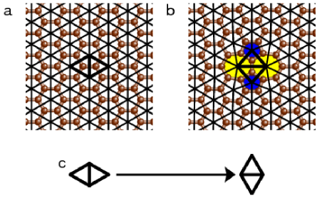
Consider for example, the Stone-WalesStone and Wales (1986) defect (Fig. 1(b)). It rotates a graphene C-C bond by 90∘. Its dual-lattice equivalent is the rotation of a patch of two joined triangles by 90∘ (Fig. 1(c)). The dual relationship between two lattices is mutual. Therefore, it is possible to design a sp2-type defect structure in “dual space” by replacing a chosen patch of the ideal triangle tiling with a different triangulated patch of the same perimeter, and then taking its dual. Metaphorically, one cuts a patch out of graphene and then “grafts” or “transplants” a different sp2-bonded patch with the same number of dangling bonds. Of particular interest is regions where the dual space replacement patch is also a portion of an ideal triangular lattice. Because the replacement structure is graphitic in this case, the formation energy should be relatively low. In such cases, one effectively has a small grain of graphene inside bulk graphene with a closed grain boundary separating the regions. We called such defects “grain boundary loops” in Ref. Cockayne et al., 2011.
There are clearly an infinite number of possible grain boundary loops in graphene. In dual space, they are described by the shapes of the (same-perimeter) triangular regions of the inner grain region “before” and “after” the procedure (Fig. 2), with the relative orientation an additional degree of freedom. Note that the “grafting” procedure provides a description of various topological defects and not how these defects actually form. This description complements an alternative description of topological defects in terms of the sequence of elementary steps (divacancies, addimers, and Stone-Wales type bond rotations) that could generate a given defect out of ideal grapheneAppelhans et al. (2010).
Using the dual space formalism, it can easily be shown that the number of dangling bonds in a graphene patch satisfies , where is the number of carbon atoms and is the number of “full” bonds in the interior. As a corollary to this formula, must be even (odd) if is even (odd). Therefore, grain boundary loops, which preserve , can only change the number of carbon atoms by a multiple of 2.
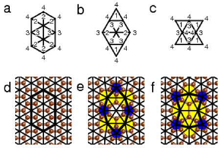
A -vertex in dual space corresponds to a -ring in graphene, that is, a ring of bonded carbon atoms. The number of bonds emanating from a vertex in dual space equals the number of triangles surrounding that vertex. The number of triangles surrounding a vertex in the defect structure equals the number of exterior triangles sharing that vertex in the “before” state plus the number of interior triangles sharing that vertex in the “after” state (see Fig. 2). Since , where is the number of “before” internal triangles, .
Studies of energies of various fullerenes containing 5-rings and 7-rings have led to the rules that the number of adjacent 5-5 pairs should be minimized and adjacent 5-7 pairs maximizedAyuela et al. (1996). A similar empirical rule has been noted for topological defects in grapheneCockayne et al. (2011); Kotakoski et al. (2011): it is energetically favorable for grain boundary loops to consist of alternating 5-rings and 7-rings. In terms of the above formula, alternating 5-rings and 7-rings are obtained if is alternately +1 and -1 for the vertices on the perimeter of the replacement triangular patch in dual space. Continuing the transplant metaphor, we define “most compatible donor(s)” for each patch of the ideal triangle lattice (if any exist), as those patches whose perimeter vertices alternately span and triangles with respect to the perimeter vertices of the original patch. Because either choice of sign is possible, a structure can have up to two inequivalent most compatible donors. Fig. 2 shows the two most compatible donors for one representative patch. The resultant defects are distinct; one reduces the number of carbon atoms by 2 and the other reduces it by 4.
We hypothesize that the most significant finite-area topological defects in graphene are grain boundary loops described by the “most compatible donor” procedure. We have enumerated all such defects with or higher symmetry that are contained within a diameter of 1.0 nm or smaller, and that change the number of carbon atoms by two or fewer. We then investigated their stabilities and predicted their scanning tunneling microscopy (STM) signatures using density functional theory.
First principles density functional theory (DFT) calculations, as encoded in the Vienna ab-initio Simulation Package (VASP) softwareKresse and Furthmuller (1996), were used perform relaxations and to calculate the local density of states for STM simulations. Vanderbilt-type ultrasoft pseudopotentialsVanderbilt (1990) were used with a plane wave basis set with a cutoff energy of 211.1 eV. Calculations were mostly performed on supercells with approximately 216 and 486 atoms. The results were extrapolated to estimate formation energies for isolated defects and their uncertainties. Efficient Brillouin zone integration was performed using a mesh containing six k-points in each supercell Brillouin zone ((1/3,0,0) and symmetry equivalents). These parameters were sufficient to obtain formation energies in good agreement with previous resultsBanhart et al. (2011). Further methodological details are given in Cockayne et al. (2011).
The in-plane lattice parameter was set to the value for graphite, corresponding to epitaxial multilayer growth conditions. Structures with more atoms than ideal graphene were allowed to relax out-of-plane, while structures with the same number of atoms or fewer atoms were fixed to remain planar. There are reports that such defects may prefer to relax out of planeMa et al. (2009). However, weak buckling instabilities might be suppressed under experimental conditions by adhesion of the surface layer in few-layer graphene to to the layer below. This is an issue for further exploration.
STM images were simulated for comparison with experimental fixed-voltage topographs. The tunneling current is approximated as proportional to the local electronic density of states integrated between and , with the Fermi level and the bias voltageTersoff and Hanann (1985). For these calculations, grids of k-points in the Brillouin zone supercell were used, centered at the origin. Using the experimental value of , the best agreement with experimental STM images in Rutter et al. (2007) comes from setting ( the Dirac level) rather than the experimental value . A significant part of the discrepancy comes from simulating a monolayer rather than the experimental case of Bernal-stacked few-layer graphene. Coupling between graphene layers in Bernal-stacked bilayer graphene raises the energy of the low-lying antibonding states of the carbon atoms on the stacked sublattice by about 0.22 eVCastro et al. (2007). Aside from the offset discrepancy, very good agreement between the monolayer simulation and the few-layer experiment is found with greatly reduced computational cost compared with multilayer DFT calculations.
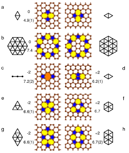
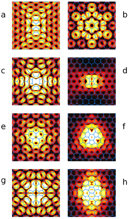
The various small high-symmetry graphene defects are shown in Fig. 3. The figures show the graphical representation of each defect, its relaxed atomic structure, the change in the number of atoms with respect to ideal graphene, and the formation energy. The structures that increase the number of atoms all have out-of-plane distortions of order 0.2 nm to 0.3 nm. Their relaxed structures have the same “rounded hill” appearance shown for such defects in the literatureLusk and Carr (2008), and are not shown here. The corresponding STM simulations of the defects are shown in Fig. 4. The height scale is larger for those structures that distort out-of-plane.
The defects shown side-by-side in Fig. 3 have graphical representations that are the inverse of each other, except for the Stone-Wales and flower defects, which are equivalent to their own inverses (as an aside, the addimer defect, frequently termed the “inverse Stone-Wales defectLusk and Carr (2008)”, is not technically the inverse of the Stone-Wales defect, but the inverse of the divacancy). Using the dual formalism, it is easily seen that if a topological defect adds atoms, its inverse removes atoms.
While the most compatible donor procedure (Fig. 2) was designed to yield structure with alternating 5 and 7 rings, in the case of the divacancy, a patch of two triangles in dual space collapses into what is effectively a zero-area polygon with 4 sides (Fig. 3(c)). The resultant structure has a new polygon, namely an 8-ring, at the center.
The most compatible donor procedure yields dual structure patches whose triangles are rotated with respect to those of the original dual. When the patches have sufficiently high symmetry, strain mismatch is minimized when the transplant patch is oriented exactly with respect to the surrounding structure. The procedure in this work thus explains the experimental observation of of rotated regions inside grain boundary loopsKotakoski et al. (2011).
Two divacancy reconstructions, and are found that are lower energy than the simple divacancy. Such energy-lowering reconstructions have previously been reportedLee et al. (2005); Banhart et al. (2011). In contrast to Banhart et al. (2011), the defect energy is lower than the one for both periodic cells investigated, although the difference between the extrapolated energies is less than their uncertainties. Since the energy of a grain boundary loop tends to increase with its perimeterCockayne et al. (2011), it is unlikely that there is any undiscovered divacancy reconstruction that has lower energy (unless it has lower symmetry than explored here).
For an addition of two atoms, the addimer defect has lowest energy. Reconstructing the addimer gives configurations that are higher in energy. Note, however, that both addimer reconstructions in Fig. 3 have appeared in numerical simulations of addimers on carbon nanotubes under strainOrikowski et al. (1999).
Topological defects can be combined to make more complex defect structures. In the dual space description nonoverlapping regions are simultaneously retriangulated. It is an open question whether and under which circumstances various topological defects attract or repel, but it is interesting that clustering has been observed experimentally for flower defectsGuisinger et al. (2008) and for divacanciesKotakoski et al. (2011).
.
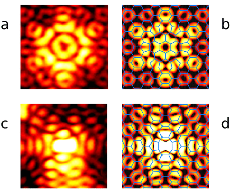
Fig. 5 shows two defects observed in experimental STM topographsRutter et al. (2007) that are well-matched by simulations of topological defects shown in Fig. 4. The sixfold defect shown in Fig. 5(a) agrees with the simulation of the flower defect (Fig. 5(b)), as previously shown in Cockayne et al. (2011). The twofold symmetric defect in Fig. 5(c) agrees very well with the simulation of the divacancy (Fig. 5(d)). The characteristic dumbbell shape of the central region was previously predicted by Amara et al.Amara et al. (2007), and distinguishes the STM image of this defect from that of the twofold symmetric Stone-Wales defect.
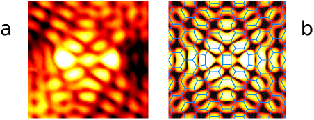
A second twofold defect observed in Rutter et al. (2007) is shown in Fig. 6(a). The double divacancy shown in Fig. 6(b) is an excellent match to the experimental image. The double divacancy has also been observed in single-layer graphene created by mechanical cleavage and then irradiatedKotakoski et al. (2011). It contains a rectangle of 4 carbon atoms in its center. Note that the simulated STM image is not simply a superposition of the STM images of two individual divacancies.
.
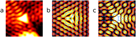
Finally, Fig. 7(a) presents the experimental STM image of a defect with threefold symmetry. This defect was initially modelled as a triple divacancy (Fig. 7(b)) in analogy with the double divacancy. The triple divacancy has a triangle of carbon atoms in the middle. While a planar triangular carbon configuration is perhaps unexpected on energetic grounds, a C-C-C triangle naturally occurs for the low-energy nonplanar bridging configuration of a single carbon adatom on grapheneMaiti et al. (1997); Li et al. (2005), and a C-C-C triangle also occurs in the cyclopropane molecule. Furthermore, the calculated formation energy of a triple divacancy in the configuration shown is 15.9 0.5 eV, less than three times the formation energy of three isolated divacancies, 7.2 0.2 eV each (Fig. 3), giving a plausibility argument for the arrangement in Fig. 7(b). (The calculated energy of the double divacancy, 11.5 0.9 eV is also less than the total for the isolated divacancies, further showing the tendency of divacancies to cluster in graphene.) The simulated STM image in Fig. 7(b) reproduces the central concave triangle seen experimentally. The peaks and nodes outside this region, however, are poorly reproduced.
An alternate explanation for the experimental threefold defect is a single vacancy (Fig. 7(c)). Although a vacancy in graphene relaxes in a way that breaks threefold symmetryEl-Barbary et al. (2003); Amara et al. (2007), the calculated local density of states between ED + 0.1 eV and ED + 0.2 eV is found to have pseudo-threefold symmetry (Fig. 7(c)). (The DFT calculations for this simulation included spin polarization to incorporate magnetism.) The electronic structure in this energy range reproduces the concave central region and furthermore, the peak and node structure outside this region matches that of the experimental STM image. The simulated image in Fig. 7(c)) looks almost exactly like that simulated for a generic impurity on the surface of graphite by Mizes and FosterMizes and Foster (1989). Their qualitative model was based on a tight-binding approximation and is equally valid for an adatom directly above a carbon, a vacancy, or a substitution. It is concluded that the threefold experimental defect is one of these three types that is located on a single carbon site. A problem with interpreting the defect as a vacancy is that, when simulated to match the experimental bias of 0.3 eV, either from ED + 0.05 eV and ED + 0.35 eV as for the other STM simulations, or for any other 0.3 eV range near , then the agreement with experiment is lost. A possible explanation for the discrepancy is strong finite-size unit cell artifacts, as the perturbation due to a vacancy falls off as Bena (2008), more slowly than for topological defects that preserve sp2 binding. STM images for a single vacancy in graphene need to be simulated for larger unit cells to test this hypothesis and compared with similar simulations for adatoms and substitutions.
In conclusion, we introduce a powerful dual space method for describing finite-area topological defects in graphene. This method allows us to systematically explore candidate low-energy defects and defect clusters. Previously unidentified defects in graphene were identified as divacancies or divacancy clusters.
Acknowledgements: I thank O. Yazyev for helpful discussions and J. Stroscio for assistance with experimental figures.
References
- Novoselov et al. (2005) K. S. Novoselov, D. Jiang, F. Schedin, T. J. Booth, V. V. Khotkevich, S. V. Morozov, and A. K. Geim, Proc. Natl. Acad. Sci. (USA) 102, 10451 (2005).
- Hernandez et al. (2008) Y. Hernandez, V. Nicolosi, M. Lotya, F. M. Blighe, Z. Y. Sun, S. De, I. T. McGovern, B. Holland, M. Byrne, Y. K. Gun’ko, et al., Nature Nanotech. 3, 563 (2008).
- Stankovich et al. (2007) S. Stankovich, D. A. Dikin, R. D. Piner, K. A. Kohlhaas, A. Kleinhammes, Y. Jia, Y. Wu, S. T. Nguyen, and R. S. Ruoff, Carbon 45, 1558 (2007).
- Yu et al. (2008) Q. K. Yu, J. Lian, S. Siriponglert, H. Li, Y. P. Chen, and S. S. Pei, Appl. Phys. Lett. 93, 113103 (2008).
- Kim et al. (2009) K. S. Kim, Y. Zhao, H. Jang, S. Y. Yee, J. M. Kim, K. S. Kim, J. H. Ahn, P. Kim, J. Y. Choi, and B. H. Hong, Nature (London) 457, 707 (2009).
- Li et al. (2009) X. S. Li, W. W. Cai, J. H. An, S. Kim, J. Nah, D. X. Yang, R. Piner, A. Velamakanni, I. Jung, E. Tutuc, et al., Science 280, 1312 (2009).
- Rutter et al. (2007) G. M. Rutter, J. N. Crain, N. P. Guisinger, T. Li, P. N. First, and J. A. Stroscio, Science 317, 219 (2007).
- Kedzierski et al. (2008) J. Kedzierski, P.-L. Hsu, P. Healey, P. W. Wyatt, C. L. Keast, M. Sprinkle, C. Berger, and W. A. de Heer, IEEE Trans. Electron. Dev. 55, 2078 (2008).
- Ugeda et al. (2010) M. M. Ugeda, I. Brihuega, F. Guinea, and J. M. Gómez-Rodríguez, Phys. Rev. Lett. 104, 096804 (2010).
- Coraux et al. (2008) J. Coraux, A. T. N’Diaye, C. Busse, and T. Michely, Nano Lett. 8, 565 (2008).
- Wofford et al. (2010) J. M. Wofford, S. Nie, K. F. McCarty, N. C. Bartelt, and O. D. Dubon, Nano Lett. 10, 4890 (2010).
- Huang et al. (2011) P. Y. Huang, C. S. Ruiz-Vargas, A. M. van de Zande, W. S. Whitney, M. P. Levendorf, J. W. Kevek, S. Garg, J. S. Alden, C. J. Hustedt, Y. Zhu, et al., Nature (London) 469, 389 (2011).
- Chen et al. (2009) J.-H. Chen, W. G. Cullen, C. Jang, M. S. Fuhrer, and E. D. Williams, Phys. Rev. Lett. 102, 236805 (2009).
- Lusk and Carr (2008) M. T. Lusk and L. D. Carr, Phys. Rev. Lett. 100, 175503 (2008).
- Lahiri et al. (2010) J. Lahiri, Y. Lin, P. Bozkurt, I. I. Oleynik, and M. Batzill, Nature Nanotechnol. 5, 326 (2010).
- Lusk et al. (2010) M. T. Lusk, D. T. Wu, and L. D. Carr, Phys. Rev. B 81, 155444 (2010).
- Terrones et al. (2010) M. Terrones, A. R. Botello-Méndez, J. Campos-Delgado, F. López-Urias, Y. I. Vega-Cantú, F. J. Rodríguez-Macías, A. L. Elías, E. M. noz Sandoval, A. G. Cano-Márquez, J.-C. Charlier, et al., Nano Today 5, 351 (2010).
- Guisinger et al. (2008) N. P. Guisinger, G. M. Rutter, J. N. Crain, C. Heiliger, P. N. First, and J. A. Stroscio, J. Vac. Sci. Tech. A 26, 932 (2008).
- Cockayne et al. (2011) E. Cockayne, G. M. Rutter, N. P. Guisinger, J. N. Crain, P. N. First, and J. A. Stroscio, Phys. Rev. B 83, 195425 (2011).
- Park et al. (2010) H. J. Park, V. Skákalová, J. Meyer, D. S. Lee, T. Iwasaki, C. Bumbry, U. Kaiser, and S. Roth, Phys. Stat. Sol. (b) 247, 2915 (2010).
- Meyer et al. (2011) J. C. Meyer, S. Kurasch, H. J. Park, V. Skakalova, D. Künzel, A. Groß, A. Chuvilin, G. Algara-Siller, S. Roth, T. Iwasaki, et al., Nature Mater. 10, 209 (2011).
- Grünbaum and Shephard (1986) B. Grünbaum and G. C. Shephard, Tilings and Patterns (W. H. Freeman and Co., New York, 1986).
- Stone and Wales (1986) A. J. Stone and D. J. Wales, Chem. Phys. Lett. 128, 501 (1986).
- Appelhans et al. (2010) D. J. Appelhans, L. D. Carr, and M. T. Lusk, New J. Phys. 12, 125006 (2010).
- Ayuela et al. (1996) A. Ayuela, P. W. Fowler, D. Mitchell, R. Schmidt, G. Seifert, and F. Zerbetto, J. Phys. Chem. 100, 15634 (1996).
- Kotakoski et al. (2011) J. Kotakoski, A. V. Krasheninnikov, U. Kaiser, and J. C. Meyer, Phys. Rev. Lett. 106, 105505 (2011).
- Kresse and Furthmuller (1996) G. Kresse and J. Furthmuller, Phys. Rev. B 54, 11169 (1996).
- Vanderbilt (1990) D. Vanderbilt, Phys. Rev. B 41, 7892 (1990).
- Banhart et al. (2011) F. Banhart, J. Kotakoski, and A. V. Krasheninnikov, ACS Nano 5, 26 (2011).
- Ma et al. (2009) J. Ma, D. Alfè, A. Michaelides, and E. Wang, Phys. Rev. B 80, 033407 (2009).
- Tersoff and Hanann (1985) J. Tersoff and D. R. Hanann, Phys. Rev. B 31, 805 (1985).
- Castro et al. (2007) E. V. Castro, K. S. Novoselov, S. V. Morozov, N. M. R. Peres, J. M. B. L. D. Santos, J. Nilsson, F. Guinea, A. K. Geim, and A. H. C. Neto, Phys. Rev. Lett. 99, 216802 (2007).
- Lee et al. (2005) G.-D. Lee, C. Z. Wang, E. Yoon, N.-M. Hwang, D.-Y. Kim, and K. M. Ho, Phys. Rev. Lett. 95, 205501 (2005).
- Qi et al. (2010) Y. Qi, S. H. Rhim, G. F. Sun, M. Weinert, and L. Li, Phys. Rev. Lett. 105, 085502 (2010).
- Orikowski et al. (1999) D. Orikowski, M. B. Nardelli, J. Bernholc, and C. Roland, Phys. Rev. Lett. 83, 4132 (1999).
- Amara et al. (2007) H. Amara, S. Latil, V. Meunier, P. Lambin, and J.-C. Charlier, Phys. Rev. B 76, 115423 (2007).
- Maiti et al. (1997) A. Maiti, C. J. Brabek, and J. Bernholc, Phys. Rev. B 55, R6097 (1997).
- Li et al. (2005) L. Li, S. Reich, and J. Robertson, Phys. Rev. B 72, 184109 (2005).
- El-Barbary et al. (2003) A. A. El-Barbary, R. H. Telling, C. P. Ewels, M. I. Heggie, and P. R. Briddon, Phys. Rev. B 68, 144107 (2003).
- Mizes and Foster (1989) H. A. Mizes and J. S. Foster, Science 244, 559 (1989).
- Bena (2008) C. Bena, Phys. Rev. Lett 100, 076601 (2008).