Anomalous enhancement of spin Hall conductivity in superconductor/normal metal junction
S. Hikino1,2S. Yunoki1,2,31Computational Condensed Matter Physics Laboratory, RIKEN ASI, Wako, Saitama 351-0198, Japan
2CREST, Japan Science and Technology Agency (JST), Kawaguchi, Saitama 332-0012, Japan
3Computational Materials Science Research Team, RIKEN AICS, Kobe, Hyogo 650-0047, Japan
Abstract
We propose a spin Hall device to induce a large spin Hall effect in a superconductor/normal
metal (SN) junction.
The side jump and skew scattering mechanisms are both taken into account
to calculate the extrinsic spin Hall conductivity in the normal metal.
We find that both contributions are
anomalously enhanced when the voltage between the superconductor and the normal metal
approaches to the superconducting gap.
This enhancement is attributed to the resonant increase of the density of states
in the normal metal at the Fermi level.
Our results demonstrate a novel way to control and amplify the spin Hall conductivity by applying an external dc
electric field, suggesting that a SN junction has a potential application for a spintronic device with a large
spin Hall effect.
pacs:
72.25.-b, 73.40.Gk, 74.55.+v, 85.75.Nn
How to generate and manipulate spin current is one of the central issues in the research field of
spintronics zutic-rev ; maekawa-book . In particular, the ability to control spin current
by an external electric field is essential because the electric field can control the flow of
electrons in nanometer scale devices. In this regard, an interaction between the spin and
orbital motion of electrons [spin-orbit interaction (SOI)] is an important ingredient.
The SOI induces the novel phenomenon called spin Hall effect (SHE),
where a charge current induces spin dependent motion of electrons, flowing perpendicular
to the charge current and in the opposite directions for up- and down-spin electrons,
and thus the spins are accumulated at the edge of the sample. The SHE has been recognized as a key effect to
convert the charge current into the spin current and vice
versa karplus ; d'yakonov ; hirsh ; zhang ; nagaosa-rev .
The SHE was first predicted theoretically decades ago, and now it is well accepted that there are
two types of SHE, the one caused by the SOI of a host metal (intrinsic SHE) karplus
and the other caused by the SOI of nonmagnetic guest impurities (most often heavy elements)
in a host metal (extrinsic SHE) d'yakonov .
For the extrinsic SHE, there are two contributions, skew scattering and side jump.
The skew scattering results from the impurity scattering via the SOI smit ,
whereas the side jump is due to the anomalous velocity induced by the SOI berger .
The first experimental observation of the extrinsic SHE has been reported by Kato ,
who have detected the spin accumulation induced by the extrinsic SHE in GaAs systems kato ; wunderlich .
Their work has stimulated extensive theoretical as well as experimental studies for the extrinsic SHE in various materials
with different experimental setups ex-she ; theory-she ; tse ; stakahashi ; seki ; koong ; guo-gu ; gradhand .
One of the important current issues is to find a way to obtain a large SHE seki ; koong ; guo-gu ; gradhand .
A large spin Hall conductivity (SHC) has an ability to generate the large spin current.
The SHC in turn depends sensitively on the SOI as well as the impurity scattering in a host material.
Very often, a larger SHE has been observed experimentally in impurity doped (extrinsic) systems rather than in
impurity free (intrinsic) systems kato ; ex-she ; morota . This is, in fact, consistent with theoretical
calculations seki ; koong ; guo-gu ; gradhand .
However, the SHE observed is still small, requiring sensitive experimental measurements to detect
the effect, in host materials such as light element metals (Al or Cu) and semiconductors kato ; ex-she .
Therefore, finding an alternative way to further increase the SHE is highly desirable, which certainly helps to achieve a variety of
SHE-based spintronic devices in the future. This is precisely the main purpose of this paper.
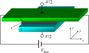
Figure 1: (Color online) Schematic configuration of a SN junction proposed to induce a large SHE.
is an applied dc voltage at the opposite edges of the N. is a
voltage applied between S and N. An insulating barrier (I) is inserted between S and N.
In this paper, we propose a simple superconductor/normal metal (SN) junction in which a large SHE is induced.
Taking into account both contributions of the side jump and skew scattering mechanisms in low impurity
concentrations, we show that the extrinsic SHC in the normal metal is anomalously enhanced when the
voltage between the superconductor (S) and the normal metal (N) approaches to the superconducting gap.
This enhancement is attributed to the resonant increase of the density of states in the N at the Fermi level.
Our results demonstrate that the SHC can be controlled and amplified by using the dc voltage,
suggesting that a SN junction has a potential application for spintronic devices with a large SHE.
The system considered is an -wave SN junction as depicted in Fig. 1.
An insulating barrier is inserted between S and N to suppress the proximity effect.
In this setup, the thickness of the N is considered thin enough to treat the N as a two dimensional N.
A dc bias voltage is applied in -direction to flow electrons in the N.
The chemical potential difference between S and N is adjusted by a dc voltage applied in -direction note .
The system is thus described by the Hamiltonian .
Here is the Bardeen-Copper-Schrieffer (BCS) Hamiltonian with an -wave superconducting gap.
represents the interaction with the applied dc bias voltage :
where and are a current operator (defined below) and a vector potential, respectively.
The gauge is set to satisfy with a spatially
uniform electric field [].
The N is described by ,
where is an annihilation operator of electron with spin at position .
and are mass of electron and the Fermi level, respectively.
The terms and describe a nonmagnetic impurity scattering and the SOI, respectively,
where is an impurity potential with the
strength locating at in the N.
is the SOI coupling and are the Pauli matrices.
For the tunneling of electrons between S and N, we adopt the tunneling Hamiltonian described by
Here, is an annihilation operator of electron in the S and the tunneling matrix element
is non zero only at the SN boundary, i.e.,
with = .
Finally, the voltage between S and N is described by the exponential factor
in .
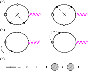
Figure 2: (Color online) The lowest order diagrams for the skew scattering (a) and side jump (b) contributions
to the spin Hall conductivity. Wavy lines denote the vector potential.
Open squares (shadow squares) are vertices of normal velocity (anomalous velocity).
Solid (open) circles represent scatterings via the nonmagnetic impurity (spin-orbit interaction) described
by (). Crosses indicate impurities.
(c) The electron Green’s function in the N up to the second order of the tunneling
matrix element.
Here large solid circles indicate the tunneling matrix element.
To evaluate the extrinsic SHC within the linear response theory,
first we consider the statistical average of the following two current operators in the -direction hosono
where
is a lesser Green’s function, and are wave numbers of electrons, and is the area of the junction.
represents the impurity average.
The lesser Green’s function is derived from the contour Green’s function,
,
where denotes the quantum statistical average at zero temperature and
is a contour ordering operator book-keldysh1 .
is the normal current, from which the skew scattering contribution is obtained,
while is the anomalous current originated from the SOI term, from which
the side jump contribution is obtained.
The SHC is obtained from
and
,
where () is the skew scattering (side jump)
contribution to the SHC, and () for up (down) electrons.
The terms and are treated
within a perturbation theory keeping the lowest order contributions, denoted by Feynman diagrams shown in
Fig. 2 (a) and (b).
This approximation is valid in a low impurity concentration .
The SHC due to the skew scattering and side jump mechanisms is then summarized as
(1)
(2)
where () is the retarded (advanced) Green’s function with zero frequency.
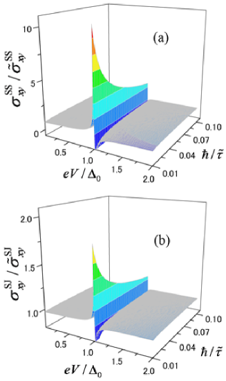
Figure 3: (Color online) Spin Hall conductivity for the skew scattering (a) and side jump (b) contributions as functions of
the voltage and the inverse relaxation time .
Here , () is the skew scattering
(side jump) contribution in the bulk N,
and a dimensionless parameter
is set to be note2 .
To calculate for the N in the SN junction, we keep the lowest contribution of the tunneling matrix
element ,
which is indicated by Dyson’s equation shown in Fig. 2 (c), and we obtain
(3)
where
is the retarded (advanced) Green’s function in the N.
is the kinetic energy of electron
and is the relaxation time due to the nonmagnetic impurity scattering within the Born approximation.
is the diagonal part of the retarded (advanced) Green’s function in the S given by
(4)
which satisfies the Gorkov’s equation.
Here, and
.
is the inelastic scattering rate in the S rodero and is the superconducting gap at zero temperature.
Substituting Eqs. (3) and (4) into Eqs. (1) and (2),
we obtain for the SHC
where () is the skew scattering
(side jump) contribution to the SHC in the bulk N with .
Let us now evaluate numerically the SHC for the two contributions derived above.
Here we take inelastic-scatt .
Fig. 3 (a) shows the skew scattering contribution to the SHC (),
normalized by the SHC for the bulk N (), as functions of
and the inverse relaxation time .
From Fig. 3 (a), it is observed that is almost the same as that of the bulk system
when deviates from .
However, when approaches to ,
becomes anomalously enhanced.
Moreover, it is seen that monotonically increases with .
Fig. 3 (b) shows the side jump contribution to the SHC (), which
exhibits the similar characteristic behavior, i.e., large enhancement of
for close to , although the enhancement factor for
appears smaller than that for .
These results clearly demonstrate that and can be significantly amplified
by tunning between S and N in the SN junction.
Next, we shall elucidate the origin of this enhancement.
To this end, it is important to notice that the extrinsic SHC is related to the electron density
of states (DOS) at the Fermi level.
The DOS at the Fermi level in the N for the SN junction considered here is obtained
by taking the imaginary part of the retarded Green’s function
(),
which is calculated by considering the same diagram shown in Fig. 2 (c).
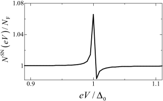
As shown in Fig. 4, the DOS for the N shows a sharp peak for close to .
This resonant increase of the DOS is simply due to tunneling of normal electrons to the S, thus reflecting the DOS of the S
which is singularly large for energy around note-tau .
Figure 4: The DOS [] at the Fermi level for the N as a function of voltage in the SN junction
at zero temperature.
Here, we take note2 and
. is the DOS at the Fermi level for the bulk N.
Let us now estimate the value of the relaxation time since this quantity determines rather sensitively
the value of the SHC as already shown in Fig. 3.
When the temperature is much lower than a typical phonon frequency, the relaxation time in the N
is mainly determined by the elastic impurity scattering. In this temperature region, the value of for the N
such as Cu and -GaAs is roughly estimated to be in a range of 10–100 ps tse ; scale .
For instance, for meV and ps,
and thus
the enhancement factor of the SHC due to the skew scattering (side jump) is as large as about 10 (less than 2). Therefore,
we expect that the anomalous enhancement of the SHC should be easily observed experimentally.
Finally, several notes are in order. First, we have considered the extrinsic SHE in this paper.
We expect the similar enhancement for the intrinsic SHE in a SN junction.
Second, it is well known that the tunneling matrix element in the SN junction is
inversely proportional to the resistance through the junction dittrich-book .
Here, only the lowest contribution of is considered, assuming that the system studied
has a comparatively high interface resistance note2 .
In such a junction, the proximity effect and the higher order contributions of are safely neglected.
However, for more quantitative analysis, details of the interface structure have to be taken into account.
Third, the spatial variation of the superconducting order parameter in the S near the interface, which has not
been considered in this study, becomes important for a small tunnel barrier
(or even for a junction with a metallic interface between S and N).
Such variation of the order parameter would affect the SHC, which remains to be studied in the future.
In summary, we have proposed a simple SN junction to induce a large extrinsic SHE.
The side jump and skew scattering contributions have been taken into account to calculate
the SHC in low impurity concentrations.
We found that both contributions are anomalously enhanced
when the voltage between S and N is adjusted close to .
This enhancement is attributed to the resonant increase of the DOS in the N at the Fermi level.
We believe that this enhancement of the SHC is large enough to be observed
experimentally culcer .
Our results demonstrate that the SHC can be controlled and amplified by using a dc electric field,
suggesting that a SN junction has a potential application for a spintronic device with a large SHE.
The authors thank S. Takahashi and Y. Niimi for valuable discussions and comments.
References
(1)
I. uti, J. Fabian, and S. Das Sarma,
Rev. Mod. Phys. , 323 (2005).
(2)
S. Maekawa, (Oxford University Press, Oxford, 2006).
(3)
R. Karplus and J. M. Luttinger, Phys. Rev. 95, 1154 (1954).
(4)
M. I. D’yakonov and V. I. Perel,
Phys. Lett A. , 459 (1971).
(5)
J. E. Hirsch, Phys. Rev. Lett. , 1834 (1999).
(6)
S. Zhang, Phys. Rev. Lett. , 393 (2000).
(7)
N. Nagaosa, J. Sinova, S. Onoda, A. H. MacDonald, and N. P. Ong,
Rev. Mod. Phys. , 1539 (2010).
(8)
J. Smit,
Physica (Amsterdam) , 39 (1958).
(9)
L. Berger,
Phys. Rev B , 4559 (1970).
(10)
Y. K. Kato, R. C. Myers, A. C. Gossard, and D. D. Awschalom,
Science , 1910 (2004).
(11)
For the first experimental observation of the intrinsic SHE,
J. Wunderlich, B. Kaestner, J. Sinova, and T. Jungwirth, Phys. Rev. Lett. , 047204 (2005).
(12)
V. Sih, R. C. Myers, Y. K. Kato, W. H. Lau, A. C. Gossard, and D. D. Awschalom,
Nature Physics , 31 (2005);
S. O. Valenzuela and M. Tinkham,
Nature , 176 (2006);
N. P. Stern, S. Ghosh, G. Xiang, M. Zhu, N. Samarth, and D. D. Awschalom,
Phys. Rev. Lett. , 126603 (2006);
T. Kimura, Y. Otani, T. Sato, S. Takahashi, and S. Maekawa,
Phys. Rev. Lett. , 156601 (2007);
L. Vila, T. Kimura, and Y. Otani,
Phys. Rev. Lett. , 226604 (2007).
(13)
M. Morota, Y. Niimi, K. Ohnishi, D.H. Wei, T. Tanaka, H. Kontani, T. Kimura, and Y. Otani,
Phys. Rev. , 174405 (2011).
(14)
R. V. Shchelushkin and A. Brataas,
Phys. Rev. , 045123 (2005);
D. Culcer, E. M. Hankiewicz, G. Vignale, and R. Winkler,
Phys. Rev. , 125332 (2010).
(15)
W. K. Tse and S. Das Sarma,
Phys. Rev. Lett. , 056601 (2006).
(16)
S. Takahashi and S. Maekawa,
Phys. Rev. Lett. , 116601 (2002);
S. Takahashi and S. Maekawa,
J. Phys. Soc. Jpn. , 031009 (2008);
H. Kontani, J. Goryo, and D. S. Hirashima,
Phys. Rev. Lett. , 086602 (2009).
(17)
T. Seki, Y. Hasegawa, S. Mitani, S. Takahashi, H. Imamura, S. Maekawa, J. Nitta and K. Takanashi,
Nat. Mater. , 125 (2008).
(18)
C. W. Koong, B. G. Englert, C. Miniatura, and N. Chandrasekhar, arXiv:1004.1273.
(19)
G. Y. Guo, S. Maekawa, and N. Nagaosa,
Phys. Rev. Lett. , 036401 (2009);
B. Gu, J. Y. Gan, N. Bulut, T. Ziman, G. Y. Guo, N. Nagaosa, and S. Maekawa,
Phys. Rev. Lett. , 086401 (2010).
(20)
M. Gradhand, D. V. Fedorov, P. Zahn, and I. Mertig,
Phys. Rev. Lett. , 186403 (2010); M. Gradhand, D. V. Fedorov, P. Zahn, and I. Mertig,
Phys. Rev. , 245109 (2010).
(21)
Note that the chemical potential of the N is equal to that of the S when .
(22)
K. Hosono, A. Takeuchi, and G. Tatara,
J. Phys. Soc. Jpn. , 014708 (2010).
(23)
Hartmut J. W. Haug and Antti-Pekka Jauho,
, (Springer-Verlag, Heidelberg, 1998).
(24)
A. Martn-Rodero, A. Levy Yeyati, and F. J. Garca-Vidal,
Phys. Rev. B , R8891 (1996).
(25)
For example, eV and meV for Nb
[B. J. Dalrymple, S. A. Wolf, A. C. Ehrlich, and D. J. Gillespie, Phys. Rev. B , 7514 (1986)],
and
eV and meV for Al
[P. Santhanam and D. E. Prober, Phys. Rev. B , 3733 (1984)].
For , e. g., see, J. P. Carbotte, Rev. Mod. Phys. , 1027 (1990).
(26)
when meV and eV .
For this , the junction resistance
is about 300 for and eV dittrich-book .
In the free electron model, the DOS at the Fermi level is for two dimensions
and for three dimensions.
Therefore, our junction has a comparatively high resistance compared with a metallic junction where the resistance is
below 1 [for instance, see, H. Yamamori, H. Sasaki, and S. Kohjiro, J. Appl. Phys. , 113904 (2010)].
Note that the results obtained in this paper are qualitatively the same for different values of .
(27)
T. Dittrich, P. Hnggi, G. -L. Ingold, B. Kramer, G. Schn, and W. Zwerger,
Quantum Transport and Dissipation, (WILEY-VCH, New York, 1998).
(28)
The apparent difference in the enhancement factors for SHC and DOS is simply because the enhancement factor for
SHC contains while that for DOS does not.
(29)
S. Takahashi, private communication.
(30)
For the experimental detection of electrical field induced spin current,
care might be taken as pointed out by D. Culcer and R. Winkler,
Phys. Rev. Lett. , 226601 (2007).