Two-junction superconductor-normal metal single-electron trap in a combined on-chip RC environment
Abstract
Dissipative properties of the electromagnetic environment as well as on-chip RC filtering are shown to suppress random state switchings in the two-junction superconductor(S) - normal metal(N) electron trap. In our experiments, a local high-ohmic resistor increased the hold time of the trap by up to two orders of magnitude. A strong effect of on-chip noise filtering was observed for different on-chip geometries. The obtained results are promising for realization of the current standard on the basis of the S-N hybrid turnstile.
1 Introduction
Experimental realization and reliable control of macroscopic quantum states require an efficient decoupling of the quantum circuit from external fluctuations. At low enough temperatures, typically mK, the role of equilibrium thermal fluctuations vanish and the dominant fluctuation mechanisms originate from residual noise photons approaching the tunneling circuit from its electromagnetic environment [1, 2]. - was regarded as a noise mechanism limiting the metrological accuracy of a normal-state single-electron tunneling (SET) pump [3]. In the superconducting state, were found to provide an influent source of decoherence, for example, in the Josephson-junction qubits [4]. More recently, (EAT) was reported to be responsible for the accuracy of a hybrid superconductor(S) - normal metal(N) single-electron turnstile [5].
On-chip filtering elements, namely a capacitively coupled ground plane and a local high-ohmic resistor, were recently demonstrated to enhance the subgap current suppression in single SIN junctions, where ”i” stands for ”insulator”, and in a two-junction hybrid SINIS turnstile [5, 6]. In our previous work [7], a Cr resistor was found to expel the quasiparticle leak in the turnstile down to the rare single-electron escape events monitored in real time by an SET electrometer. Our present study addresses both partial contributions and the integral effect of the aforementioned improvements in a combined RC environment of a two-junction SINIS trap. Different sample geometries are analyzed with regard to the suppression of noise-activated tunneling and possible propagation ways of the noise photons.
2 Experiment and results
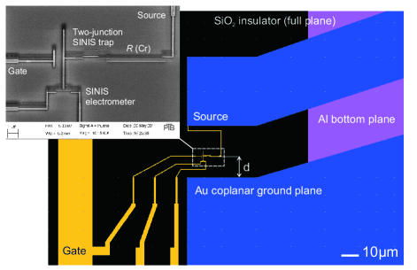
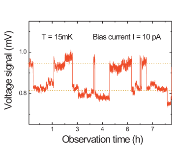
Our trapping device, shown in the inset to Fig. 2, included a two-junction SINIS turnstile, either with or without a high-ohmic Cr resistor on the source side, and a dc-SET SINIS electrometer. The electrometer was coupled capacitively to the opposite, open-end terminal of the turnstile, used as an electron trapping reservoir with discrete states. All four SIN(NIS) junctions were nominally of the same area, which was used in estimating the parameters of the turnstile: the charging energy , where is the capacitance of a tunnel junction, the tunnel resistance , and the superconducting gap of the Aluminum S leads eV, based on those data obtained for the electrometer. Similar to the experiment in Ref. [7], the electrometer was used to record the random state switchings of the trap, see an example in Fig. 2, and, in this way, to quantify the electron escape process across the Coulomb energy barrier in the turnstile. In particular, the average switching interval (hold time) was assumed to be inversely proportional to the escape rate and, determined for the trap adjusted to its maximum Coulomb barrier , could be compared with our follow-up of the EAT model developed in Refs. [2, 5].
The devices under test were fabricated on thermally oxidized silicon substrates using the three-shadow evaporation process described previously in Ref. [7] and the references therein. That formerly developed process included the fabrication of a 50 nm-thick coplanar ground plane (CGP) of Au, which was also common for all the samples reviewed here (see Fig. 2). For the present study, every circuit - except the Sample 4 - was built on top of a 50 nm-thick bottom plane (BP), either of Al or AuPd, covered by a 200 nm-thick insulating layer of SiO2. The capacitance 100 pF of each dc lead to the bottom plane together with the lead resistance , formed an effective low-pass filter for the external noise with the cutoff frequency, 10—100 MHz, well below the excitation threshold for quasiparticles 50 GHz. The trapping devices were positioned above an opening in the bottom plane at different distances to the closest grounding element, as shown in Fig. 2 and in Table 1. The resistance of our 5 m-long Cr resistor was estimated using an identical test resistor on the same chip. For the circuits without a Cr resistor, the lead impedance was accepted being on the scale of 1 k.
| \brSample No. | CGP/BP | m | ||||
| \mr1a | \0250 | \0150 | 150 | CGP+BP(Al) | 200 | \m0.3 |
| 1b | \0250 | \0150 | 1 | CGP+BP(Al) | 200 | 0.05a |
| 2a | \0250 | \0400 | 150 | CGP+BP(AuPd) | 200 | \0 1.0 |
| 2b | \0250 | \0400 | 1 | CGP+BP(AuPd) | 200 | \0 0.2 |
| 3a | \0500 | \0800 | 150 | CGP+BP(AuPd) | 200 | \m500 |
| 3b | \0500 | \0800 | 1 | CGP+BP(AuPd) | 200 | \m2–5 |
| 4 | 1000 | 1850 | 440 | CGP | 200 | \0200 |
| 5 | \0300 | \0400 | 550 | CGP+BP(Al) | \010 | 2200 |
| \br |
aThe frequency of switchings exceeded the detection bandwidth of the dc electrometer.
The experimental results are summarized in Table 1. They were obtained at the base temperature of our dilution fridge 15 mK, using a microwave-tight (but not hermetically-sealed) sample holder equipped with 1—1.5 m-long Thermocoax coaxial filters per each dc-line. The structures indexed as ”a” and ”b”, located on the same sample and differing only by the value of , were measured within the same low-temperature cycle, which made possible a direct comparison of an effect of the low- and high-ohmic environment.
3 Model and discussion
We interpret our data in the framework of the EAT model [5, 7]. We assume a black-body radiation noise of the environment, equilibrated at the temperature level of the closest radiation shield, 1 K, being the most probable source of higher-energy excitations. It is further assumed that the S leads are originally free of quasiparticles (see, e.g., Ref. [8]), and the dominant recharging cycles start with an electron tunneling from the N island, as depicted in the inset in Fig. 3, and producing a quasiparticle in the S node of the trap. This energetically unfavorable process is stimulated by the voltage noise across the SIN junctions, and we model the noise effect by introducing a phenomenological non-equilibrium population of states above the Fermi-level in the normal metal, . In our approximate model, the dimensionless noise intensity pre-factor is accepted being independent on the parameters of the trapping device itself, but solely related to the noise properties of the environment.
For the rate calculation, we make use of the very low temperatures of both S and N leads, , which reduces the golden-rule tunneling formula to the simplified zero-temperature case:
| (1) |
where is the BCS density of states in a superconductor and the function , the absorption spectrum of the environment, is that for the pure ohmic environment at zero temperature [2]. An electron escape across the turnstile is completed by tunneling through the second SIN junction at much higher rate, thus making the onset rate defined in equation 1 the dominant term in the overall escape rate: . The tunneling rate appears in equation 1 proportional to the noise pre-factor , so the hold time of similar trapping devices should provide a direct measure of the on-chip noise suppression through .
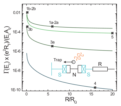
Figure 3 predicts a reduction of the tunneling rate by increasing the resistance . There is a reasonable agreement with the hold times in Samples 3a and 3b and still quantitative deviation from the data obtained for Samples 1a,b and 2a,b. In particular, an increase up to 500 s due to = 150 k is as high as by two orders of magnitude between Samples 3a and 3b. Within the sample pairs 1a,b and 2a,b with a lower value of 250 eV and 1 s, the model predicts factor 3 smaller ratios of the hold times. Nevertheless, the experimental ratios were found to be even smaller than the predicted ones, presumably, due to the finite frequency bandwidth of our detector.
A pronounced effect of the bottom plane was observed in the comparison of Sample 5 to Sample 4. Taking into account the calculated data shown in Fig. 3 as well as the experimental data in Table 1, one can conclude on the ratio as an effect of the bottom plane. A further comparison of Samples 5 and 3a, positioned at a larger distance to the large-area planes, indicates noise suppression by factor in vicinity of the shielding planes. Since for both samples the on-chip filtering design is identical, we conclude on the space propagation channel for the noise photons. Finally, we note that the derived relative values of depend exponentially on the measured uncertainties in and and need more direct confirmation.
To conclude, a hold time of an SINIS trap was measured for various specially engineered on-chip electromagnetic environments. The combined effect of both the high-ohmic resistor and the improvement in the sample geometry (Samples 2b and 5) manifested itself in the hold time increase by about four orders of magnitude. Strong partial effects of both the high-ohmic resistor and the on-chip RC filtering (bottom plane) were observed. Further experiments are in progress to quantify the effect of the sample design on the noise-activated tunneling processes.
Fruitful discussions with J Pekola and A Kemppinen are gratefully acknowledged. Technological support from T Weimann and V Rogalya is appreciated. The research conducted within the EU project SCOPE received funding from the European Community’s Seventh Framework Programme under Grant Agreement No. 218783.
References
References
- [1] Averin D V and Likharev K K 1991 Mesoscopic Phenomena in Solids (Amsterdam: Elsevier) pp 173-271
- [2] Ingold G L and Nazarov Yu V 1992 Single Charge Tunneling, Coulomb Blockade Phenomena in Nanostructures (NATO ASI Series B vol 294)(New York: Plenum Press) ch 2
- [3] Kautz R L, Keller M W and Martinis J M 2000 Phys Rev B 62 15888
- [4] Lang K M, Nam S, Aumentado J, Urbina C and Martinis J M 2003 IEEE Trans. Appl. Superconduct. 13 989
- [5] Pekola J P, Maisi V F, Kafanov S, Chekurov N, Kemppinen A, Pashkin Yu A, Saira O-P, Möttönen M and Tsai J S 2010 Phys Rev Lett 105 026803
- [6] Lotkhov S V, Kemppinen A, Kafanov S, Pekola J P and Zorin A B 2009 Appl Phys Lett 95 112507
- [7] Lotkhov S V, Saira O-P, Pekola J P and Zorin A B 2011 New Journ Phys 13 013040
- [8] Saira O-P, Kemppinen A, Maisi V F and Pekola J P 2011 Is aluminum a perfect superconductor? arXiv:1106.1326v1