Observation of drift and diffusion processes
in Ti/TiOx/Ti memristive devices
prepared
by tip-induced oxidation
Abstract
We demonstrate that memristive devices can be fabricated by tip-induced oxidation of thin metallic films using atomic force microscope. Electrical measurements of such prepared Ti/TiOx/Ti test structures confirmed their memristive behavior and inferred diffusion of oxygen vacancies in the TiOx barrier. Consequent Kelvin probe force microscopy studies provided evidence for the diffusion, as well as for expected oxygen vacancy drift. Time evolution of the space distribution of the vacancies due to the diffusion process revealed minute-scale (at least) retention times of the devices. The work presents technology alternative for fabrication of memristive nanodevices in geometry favouring advantageous scanning probe microscopy studies of their in-barrier processes, as well as widely utilizable approach to search for novel oxide materials for perspective memristive applications.
Four decades ago Chua provided strong arguments [1] that besides the resistor, inductor, and capacitor, there should exist one more fundamental passive circuit element, so-called memristor (shortcut for memory resistor). A characteristic property of this two terminal device is its resistance, which depends on history of the current passing through it resulting in hysteretic current-voltage (-) curves. Although over time many observations of hysteretic - curves were reported, connection of this phenomenon with memristive behavior was done only recently by Strukov and co-workers [2], who shoved, that memristance arises naturally in nanoscale systems in which solid-state electronic and ionic transport are coupled under an external bias voltage [2]. As typical representatives of memristive devices can be considered metal/oxide/metal two-terminal nanodevices, and Pt/TiO2/Pt nanodevices (exhibiting bipolar resistive switching) seem to be a prototypical (nano)structure exhibiting memristive behavior. Based on experimental studies of TiO2 junction devices with platinum electrodes it was established that electrical conduction in metal/oxide/metal thin-film devices is controlled by a spatially heterogeneous metal/oxide electronic barrier [3], and memristive electrical switching proceeds by means of the drift of positively charged oxygen vacancies acting as native dopants to form (turn ON) or disperse (turn OFF) locally conductive switches through the electronic barrier [3].
Although metal/oxide/metal type devices exhibiting memristive/resistive switching are intensively investigated for very long time (especially because of their potential use in non-volatile memory applications), and significant progress in the field was done after ”rediscovery” of the memristor [2, 3, 4, 5, 6, 7, 8, 9, 10, 11, 12], there are still many open questions related to local physical and chemical properties in the oxide barrier region [13]. Many of these peculiarities arising at nanoscale could be very effectively studied by various advantageous scanning probe microscopy (SPM) techniques. For instance, Kelvin probe force microscopy (KPFM), which measures contact potential between the sample and a (metal coated) tip of atomic force microscope (AFM) [14], and is obviously used for direct detection of the work-function changes in metals or doping-level changes in semiconductors [14, 15], could provide valuable information about space distribution of oxygen vacancies in the active regions of the nanodevices. Unfortunately, SPM studies of oxide-barrier processes in this kind of nanodevices is a non-trivial task, such as they are as a rule prepared in vertical, stacked geometry with oxide layer between a top and a bottom electrode [3, 7, 16]; thus removing of the ”top” electrode is necessary to enable direct observation of the oxide barrier by SPM [16]. Stacked geometry of the memristive devices has at least one more negative aspect; it requires specific, often very expensive equipment that might be a limitation for widespread use in searching for new materials for perspective memristive applications. Therefore, new approaches enabling simple preparation of memristive devices in geometry suitable for use of SPM-based techniques to study the processes in the oxide barrier are highly desired for faster progress in the field.
Interesting technology alternative for definition of oxide patterns with resolution in the nanoscale is local anodic oxidation (LAO) by use of AFM, which is well-established method for tip-induced oxidation of semiconducting [18] and metallic [17] surfaces. The method was succesfully used to fabricate many nanoelectronic and nanophotonic devices, e.g. metal/insulator/metal (MIM) type nanodevices, single-electron transistor, or a photoconductive switch [19]. Important advantage of this method is lateral planar geometry of devices fabricated this way, which enables realization of studies of the oxidized regions by desired SPM techniques.
The aim of this work is to demonstrate that LAO can be effectively used also for fabrication of metal/oxide/metal (MIM) type devices exhibiting memristive behavior. In the presented case study Ti/TiOx/Ti structures were prepared such as TiO2 (an important fraction of TiOx formed in the LAO process [19]), is a prototypical memristive material [13]. Consequently, KPFM was used to perform direct experimental observations of oxygen vacancy movement in the TiOx region.
For purposes of this work, MIM type devices on the base of Ti thin films were prepared as follows. First, microbridges (6-8 nm thick, 30-80 m wide, 100-300 m long) were deposited by DC magnetron sputtering on glass substrates kept at ambient temperature. The sputtering was done from polycrystalline Ti target at Ar-pressure of 3 mTorr and rate of 0.04 nm/s. A shadow mask was used to define the bridges. Oxide barrier across the bridge was fabricated by LAO using AFM equipped with commercial nanolithography software. The oxidation process was performed in contact mode at ambient conditions with relative humidity between 55 and 60 %. To ensure oxidation up to the substrate, the lines across the bridge were overwritten several times like described in Ref. 17, 20. The width of the formed TiOx lines varied between 400 and 1200 nm. Resistance of the films/microbridges before the oxidation was of order of tens of k; during the oxidation process, while forming Ti/TiOx/Ti structure, the resistance increased typically more than three orders of magnitude. KPFM studies of the Ti/TiOx/Ti structures were done in passive state (with both Ti electrodes grounded), as well as in active state (with bias voltage applied to one of the electrodes while the other one was grounded). For electrical characterization of the devices bias voltage, , was applied to the prepared structure and the current, , flowing through it was measured.
First electric characterization of the Ti/TiOx/Ti devices was done by measuring the - curves at both increasing and decreasing , at applied triangular excitation voltage signal of a period not longer than a few tens of seconds. Recorded curves (see inset in Fig. 1) show almost symmetric characteristics strongly resembling tunneling between two identical metals.
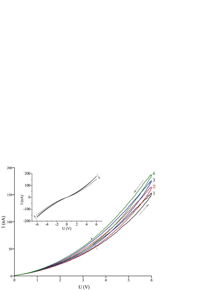
In addition, the curves reveal very small hysteresis, and a small decrease of the slopes, as shown in the inset of Fig. 1. These small, but well detectable changes reveal a change of the device conductance state due to the applied bias and are interpreted as a sign of memristive behavior. Considering a physical model of the memristor [4, 2] a small hysteresis can be adequately interpreted as a consequence of small change of oxygen vacancy distribution in the TiOx region during one period of the applied voltage, what indicates relatively ”fast” ramping of the bias voltage [4, 2]. Exciting the device by positive voltage with sinusoidal modulation and DC offset equal to the amplitude of the sinusoidal waveform [, where is time and is the period (now in the range of hundreds of seconds)], a sequence of - loops clearly resembling behavior expected for the memristor [2] was observed, as can be seen in Fig.1. - curves from four consequtive positive voltage sweeps show a continuous increase in conductance, but also an overlap of the loops was observed. This is very similar observation like recently reported for Pd/WO3/W devices [21], interpreted as a consequence of oxygen vacancy diffusion (in addition to their drift under electric field) [21]. The relevance of such interpretation was adequately supported by simulations [21] using the SPICE model of the memristor [22] incorporating both drift and diffusion into the model [21]. To interpret the observed overlap of - loops in the Ti/TiOx/Ti devices, we adopt qualitatively the same interpretation (i.e. we consider that in addition to the drift of oxygen vacancies also their diffusion is substantional), what we support by KPFM studies as described below.
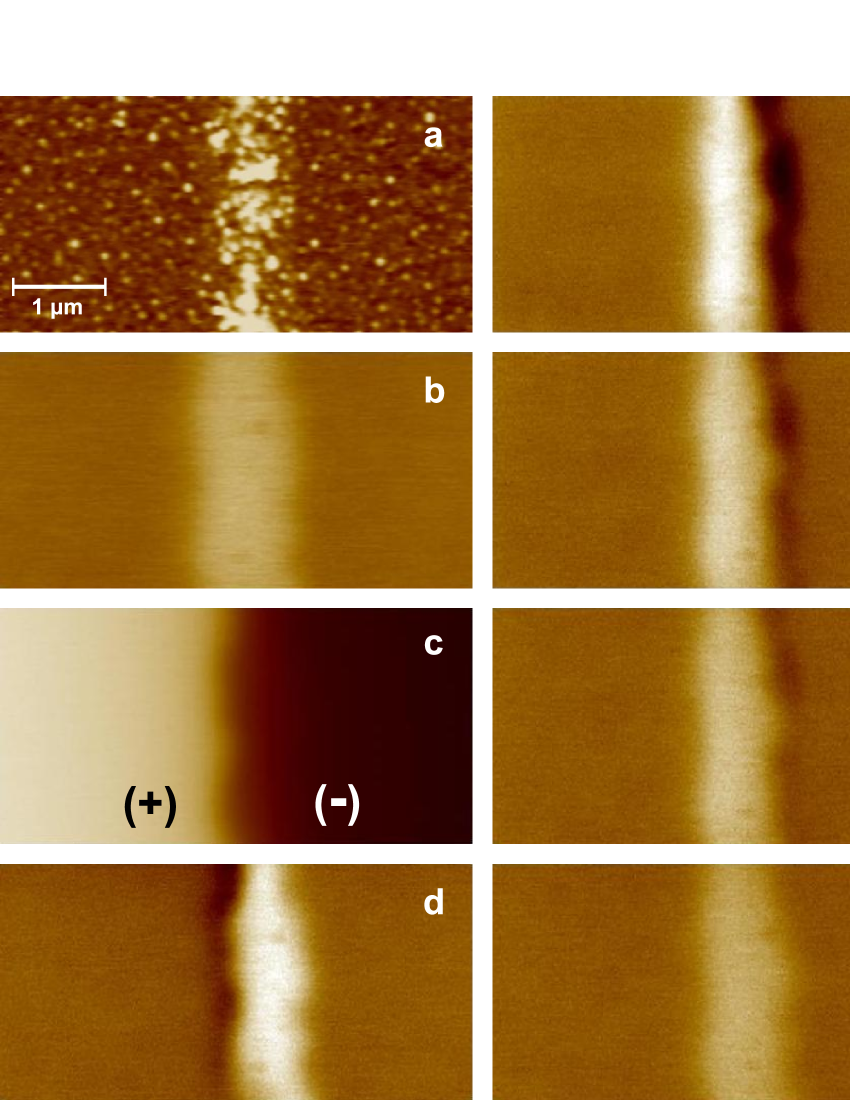
Initially, KPFM studies of Ti/TiOx/Ti structure were done with both Ti electrodes grounded. Topography image of the region in the vicinity of the oxide barrier is shown in Fig. 2a, while Fig. 2b shows the corresponding surface potential distribution measured by KPFM. Such as the measurements were performed after the above mentioned electric studies and no cleaning process was done to prevent change of the oxide barrier properties, the topography image reveals quite degraded and contaminated surface. In spite of this, the surface potential image clearly reveals oxidized region of the width 1000 nm, seen as a brighter region with higher surface potential than that of Ti electrodes. Consequently, the bias voltage was applied between the Ti electrodes and surface potential was measured for several values of the applied voltage in the range of V. As demonstrated in Fig. 2c, at applied bias voltage of 3 V (negative Ti electrode - cathode - is seen as a dark region) change of the surface potential is dominanting in the oxide barrier region. After the removal of the the bias voltage +3 V the surface potential image (Fig. 2d) reveals formation of a wide region of increased surface potential in the oxide barrier on the side closer to the cathode (bright region on the right side of the barrier), and a narrow region with pronounced decrease of the potential on the opposite side of the oxide barrier (dark region closer to the Ti electrode that was biased positively - anode). The increase of the surface potential in the barrier region we associate with increased concentration of positively charged oxygen vacancies, which drifted upon the applied voltage towards the cathode. The decrease of the surface potential on the opposite side of the barrier we link to decreased concentration of positive oxygen vacancies and increased concentration of negative oxygen ions in the vicinity of the anode. (Note that concentration of negative oxygen ions in the vicinity of the anode can be also affected by formation of O2 gas, such as negative oxygen ions drifting to the anode can be discharged to form O2 gas there, as can be deduced from the results of electroforming studies of Pt/TiO2/Pt devices [16, 24].) Applying bias voltage of the opposite polarity (-3 V) for several minutes (not shown) leads to inverse surface-potential picture (Fig. 2e), thus confirming a voltage-driven drift of oxygen vacancies during the application of bias voltage. As can be seen in figures 2e-h, the voltage-induced regions of higher/lower surface potential vanish with time, revealing equilibration process of the vacancy concentration in the barrier. In accordance with the above discussed indications from the overlap of - hysteresis loops we interpret the observed equilibration process as a consequence of oxygen vacancy diffusion. Nearly uniform surface potential, indicating almost uniform distribution of oxygen vacancies in the barrier was observed again approximately an hour after the removal the bias voltage, as can be seen in Fig. 2h.
The above mentioned KPFM observations are considered as a direct evidence for the vacancy drift and diffusion in Ti/TiOx/Ti memristive structures. The corresponding time constant of the diffusion process is estimated to be of order of tens of minutes. Such as the diffusion process in fact defines the time scale at which the device is capable to store an information, or when it loses its state [23], the results of KPFM can also be interpreted as indication for minute-scale (at least) retention times of the Ti/TiOx/Ti memristive devices. Such retention times are applicable e.g. in bio-inspired circuits [23].
Here we would like to mention that in accordance to our knowledge the above presented results represent first investigation of memristive device(s) fabricated by local anodic oxidation, as well as first direct experimental evidence for both vacancy drift and diffusion in the active part of a memristive device. Moreover, the results provide an experimental support for the model proposed by other authors [21], who incorporated both drift and diffusion effects into their SPACE simulation to explain the observed memristive behaviors of Pd/WO3/W devices. The results also infer that KPFM can be used for quantitative characterization of the diffusion processes in nanodevices by scanning the time evolution of the surface potential of the relevant part of the nanodevice after the removal of the voltage applied to the device. For studies of relatively slow diffusion processes a repetitive scanning can be done for relatively larger area just as done in this work. However, if more detailed information or highest ”sampling” rates of the scan region is required, then scanning process can be reduced just to one scan line. The later approach should be preferred also in studies where the most detailed information about the diffusion dynamics in the selected surface cross-section of the active part of the device is required.
Important technological impact of the presented work is that it shows a simple approach to search for new oxide materials with potential use in memristive applications (e.g. those for memristive/resistive switching ones). Such materials can be grown in the process of LAO, where very diverse materials can be used as precursors for the oxidation. This approach is especially suitable for synthesis of complex oxides, e.g. by oxidation of multicomponent thin films. For instance, thin film precursors can be prepared by magnetron co-sputtering from several targets, or may consist of several layers of different materials deposited/grown by any desired thin film technique. Feasibility tests of oxide materials grown in the barrier of MIM structure can be then done by means of electric measurements or/and by relevant SPM studies.
The described approach brings also interesting possibilities to studies of electroforming, what is important technological step used to initialize resistive switching process in many oxides [16, 24, 25, 26, 27, 28, 29, 30]. Especially studies of electroforming combined with advantageous SPM studies could shed some light on the processes in the oxide barrier that are responsible for initiation of resistive switching. (Note that no electroforming was performed for Ti/TiOx/Ti structures reported here, but preparation of such experiments is in progress.)
In summary, we managed to fabricate Ti/TiOx/Ti devices exhibiting features of memristive behavior using the tip-induced oxidation, thus providing geometry favourable for investigations of phenomena in the oxide barrier by use of SPM techniques. Performed electric measurements revealed memristive behavior of the devices, and indicated importance of diffusion processes in the TiOx barrier. Kelvin probe force microscopy studies provided direct evidence for voltage-induced drift and consequent diffusion of oxygen vacancies, and revealed retention times of the devices at minute-scale, thus inferring that KPFM can be used for quantitative characterization of the diffusion processes in materials and nanodevices. The presented approach represents a favorable technology alternative for routine fabrication of memristive devices and investigation of physical phenomena in the active part of the device by use of advantageous SPM techniques. Such as MIM type structures with many new oxide materials in the oxide barrier can be routinely fabricated by tip-induced oxidation, we believe that presented approach will be widely used to seek for new oxide materials for perspective memristive applications.
Acknowledgments
This work was supported by the Slovak Scientific Agency VEGA under the contract No. 2-0133-09, and by the ERDF EU (European Union European regional development fond) grants, under the contract No. ITMS 26220120005 and ITMS 26220120047.
References
References
- [1] Chua L O 1971 IEE Trans. Circuit Theory 18 507
- [2] Strukov D B et al 2008 Nature (London) 453 80
- [3] Yang J J et al 2008 Nat. Nanotechnol. 3 429
- [4] Pershin Yu V and Di Ventra M 2011 Adv. Phys. 60 145
- [5] Kwon D-H et al 2008 Nat. Nanotechnol. 3 429
- [6] Strachan J P et al 2011 Nanotechnology 22 254015
- [7] Xia Q et al 2011 Nanotechnology 22 254026
- [8] Robinett W. 2010 Nanotechnology 21 235203
- [9] Medeiros-Riberio G 2011 Nanotechnology 22 095702
- [10] Waser R and Aono M 2007 Nat. Mater. 6 833
- [11] Yang J J et al 2009 Adv. Mater. 21 3754
- [12] Strachan J P et al 2010 Adv. Mater. 22 3573
- [13] Szot K 2011 Nanotechnology 22 254001
- [14] Nonnenmacher N et al 1991 Appl. Phys. Lett. 58 2921
- [15] Melitz W 2011 Surface Science Reports 66 1
- [16] Yang J J et al 2009 Nanotechnology 20 215201
- [17] Irmer B et al 1997 Appl. Phys. Lett. 71 1733
- [18] Snow E S et al 1993 Appl. Phys. Lett. 63 749
- [19] Matsumoto K 1997 Proc. IEEE 85 612
- [20] Šoltýs J. et al 2003 Acta Phys. Polonica A 103 553
- [21] Chang T et al 2011 Appl. Phys. A 102 857
- [22] Biolek Z et al 2009 Radioengeneering 18 210
- [23] Strukov D B and Wiliams R S 2009 Appl. Phys. A 94 515
- [24] Jeong et al 2008 J. Appl. Phys. 104 123716
- [25] Choi B J et al 2005 J. Appl. Phys. 98 033715
- [26] Jeong D S et al 2007 Electrochem. Solid-State Lett. 10 G51
- [27] Gibbons J F and Beadle W E 1964 Solid-State Electron. 7 785
- [28] Hickmott T W J. Vac. Sci. Technol. 6 828
- [29] Szot K et al 2006 Nat. Mater. 5 312
- [30] Oligschlaeger R. et al 2006 Appl. Phys. Lett. 88 042901